Quantum dot-based device for high-performance magnetic microscopy and spin filtering in the Kondo regime
Abstract
We propose a nanoscale device consisting of a double quantum dot with a full exchange and pair hopping interaction. In this design, the current can only flow through the upper dot, but is sensitive to the spin state of the lower dot. The system is immersed in a highly inhomogeneous magnetic field, and only the bottom dot feels a substantial magnetic field, while the top dot experiences only a residual one. We show that our device exhibits very interesting magnetic field-dependent transport properties at low temperatures. The Kondo effect partially survives the presence of the magnetic field and allows to obtain conductances that differ by several orders of magnitude for the two spin types across the top dot. Interestingly, as a function of the magnetic field, our two-dot device changes from a spin singlet state to a spin triplet state, in which the amplitudes of the spin-dependent conductances are reversed. Our device is able to discriminate between positive and negative magnetic fields with a high sensitivity and is therefore particularly interesting for imaging the surface of anti-ferromagnetic (AF) insulating materials with alternated surface magnetic field, as well as for spin filtering applications.
Magnetic structure of matter is a fascinating field, where a large variety of orders can be observed. In addition to ferromagnetic and antiferromagnetic orders, competing magnetic interactions give rise to very interesting complex non collinear spin states [1]. Contrasting with ferromagnetic materials, in materials where antiferromagnetic interaction is dominant, it is often possible to switch magnetic moments at low energy cost. This can be promising for low-energy spintronic devices [2]. Spin filtering is another important ingredient of spintronics which may be realized with our proposal of capacitively coupled quantum dots. Spin filtering in transport processes via quantum dots had been proposed already several times [3, 4, 5, 6, 7] but our proposal is interesting since one can reach very high polarizability as we will demonstrate in the following.
Nevertheless, investigating the magnetic properties of these materials is a difficult task because local magnetic moment is either very small or oscillating at small length scales and they display insulating properties. Indeed, magnetic force microscopy (MFM) is adapted to insulating materials and can be used to unravel the magnetic properties of nanomaterials applied in biological systems and future directions for quantum technologies [8]. Unfortunately its sensitivity is not sufficient to detect very low or rapidly oscillating magnetic fields existing in antiferromagnets. Spin-polarized scanning tunneling microscopy is a much more sensitive technique and is a powerful technique to probe nano- and atomic-scale magnetism [9]. However, it is restricted to conductive materials.
Real space imaging using a single-spin magnetometer based on a single nitrogen–vacancy (NV) defect in diamond has been shown to be very efficient for imaging complex antiferromagnetic orders at the nanoscale [10]. The obtained image showed a spin cycloid in a multiferroic bismuth ferrite (BiFeO3 ) thin film with a period of about 70 nanometers, consistent with values determined by macroscopic diffraction. However, a biased field has to be applied to determine the sign of the measured magnetic field. This applied magnetic field could influence the fragile magnetic structure of the sample.
Here we propose a quantum dot-based device which is able to measure the local magnetization existing in the close proximity of an antiferromagnetic sample surface. Our device does not need any external applied magnetic field and takes advantage of the high sensibility of the Kondo effect.
Quantum dots can be used as highly sensitive magnetic field measurement. Recently, graphene quantum dots show promise as novel magnetic field sensors [11] by using confined massless Dirac fermions in electrostatically defined QDs.
Kondo effect plays a crucial role in transport properties of quantum dots. In the Coulomb blockade regime [12, 13, 14, 15, 16], the low temperature restoration of the conductance is one of the most spectacular manifestation of this effect. The sharpness of the zero-bias resonance in the differential conductance [17, 18, 19, 21, 20, 22, 23], opens up a wide range of highly sensitive applications using the Kondo effect for the development of molecular electronics [24, 25], for example.
Like other quantum phenomena, the resonant spin-flip correlations underlying the Kondo effect are limited to very low temperatures and persist only up to some tens of milli-Kelvin in the usual semiconductor-based devices, or at best some tens of Kelvin in molecular electronics [24, 26], although Kondo temperatures as high as have been reported for magnetic impurities on surfaces [27, 28].
Besides its temperature dependance, the magnetic nature of the Kondo effect implies also a strong external magnetic field dependance. The interplay of Kondo effect and applied magnetic field has been studied in many previous works. For example, nonequilibrium Kondo transport through a quantum dot in a magnetic field has been investigated in 2013 [29] and more recently, magnetic field induced Kondo effect that takes place for level crossings in finite Co chains has been studied by Danu et al. [30] Temperature and magnetic field dependence of a Kondo system in the weak coupling regime has been investigated experimentally for organic molecules weakly coupled to a Au (111) surface, showing a splitting of the resonance in magnetic field [31]. More recently, experimental results on a molecular quantum dot in the Kondo regime demonstrate that the bias-dependent thermocurrent is a sensitive probe of universal Kondo physics, directly measuring the splitting of the Kondo resonance in a magnetic field [32].
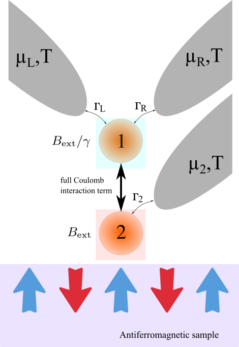
The possibility of observing electron transport governed by the Kondo effect with an applied magnetic field is made possible here by the strong magnetic field gradient existing in the vicinity of the surface of the antiferromagnetic material. The device proposed in this Letter is schematically depicted in Fig. 1. The conductance across the first dot, labeled 1 (conduction channel) allows to measure the magnetic leakage field of the sample . The second dot, labelled 2, is able to get very close to a magnetized sample and is therefore immersed in while dot 1 experiences . The electronic occupation of dot 2 is therefore expected to be strongly spin dependent, which ultimately pilots a spin polarized current across dot 1 via interdot Coulomb interactions. The full Coulomb interaction term contains exchange coupling and pair hopping processes and consequently correlates spin dependent properties of dot 1 and 2. Experimental realization of capacitively coupled quantum dots without interdot net tunneling have already been achieved e.g. in GaAs/AlGaAs heterostructures [33, 34], and tunable interdot couplings with minimal residual interdot tunneling were implemented using bilayer graphene on silicon substrate [35].
We will show in the following that the present double-quantum dot setup not only offers the possibility to construct a quantum device capable of measuring surface magnetic field but can also be used to generate an almost pure spin-current.
To investigate the setup proposed in Fig. 1, we will study the corresponding single-impurity Anderson model [36] within the framework of the non-crossing approximation (NCA) [37, 38, 39]. The model’s electronic Hamiltonian contains contributions from the leads, the dots, and from tunneling between leads and dots, . The three uncorrelated metallic leads, , are described by
| (1a) | |||
| with and the creation and annihilation operators of -electrons in state on the lead . The contribution from the dots is [40] | |||
| (1b) | |||||
where is the total electronic occupation on dot , with the number of -electrons on the dot, and () the corresponding creation (annihilation) operators. The sum in the above expression thus describes two individual Anderson dots, with the dot 2 serving as a magnetic gate, and the dot 1 defining the conduction channel. Eq. (1b) accounts for the full interaction term between both dots and can be implemented experimentally as described in Refs. 33, 34, 35. and are the spin dependent energy levels of the dots, including Zeeman splittings due to external magnetic fields for dot 1 and for dot 2. We have and . In the following we take to take account of the inhomogeneity of the magnetic field at the surface of the antiferromagnetic material, and to reduce the number of independent parameters, but it would be entirely possible to control these two energy levels independently. The operator is the -spin operator for dot . The parameters denote the repulsions between electrons occupying the same dot , is the repulsion between electrons occupying different dots, is the Hund exchange term, and is the double hopping term. This last term is systematically present when exchange interactions take place. Note that the Hamiltonian is relevant for double-quantum dots and for single quantum dot with two orbitals, however there is no reason to enforce invariance under rotation in the orbital space for the double-quantum dots, and the constraints and are not required.
Finally, the lead-dot tunneling is given by
| (1c) |
where the first line describes the coupling of electrons on dot 1 to the left and right lead, while the second line allows electrons on dot 2 to tunnel to the third lead. For most practical cases, the tunneling amplitudes only depend on via the corresponding level energy, , such that the tunneling to each lead is entirely summarized by the hybridization strength [41] where is the spin-summed DOS on lead (). Here, we further assume that all three leads are identical metals, with a DOS characterized by a single wide band, and that the tunneling between any lead and its dot is governed by the same only weakly energy-dependent physical process such that all three hybridization strengths are the same, . Specifically, we take broad Gaussian lead DOSes, of half-width , where is the total hybridization strength of the lower dot at the mean chemical potential . will henceforth serve as our energy unit which, with set to unity and the Bohr magneton set to 2, will also be our unit of temperature and magnetic field. Furthermore, we assume zero voltage and temperature bias such that and .
The spin dependent conductance is given in terms of spin resolved energy-weighted integrals [42],
| (2) |
The integrand comprises the spin dependent Fermi function, , and the equilibrium transfer function, . Similarly, the occupancies of the dots also follow from the lead Fermi functions and the dot spectral functions via [43]
The are readily obtained from the corresponding retarded dot Green’s functions . In the atomic limit, the dot Green’s functions would show sharp transitions between the 4 local eigenstates of each dot. The hybridization with the leads and the interdot Coulomb repulsion, however, create correlations and fluctuations between these 16 local states, and we address the latter within the framework of the NCA, an approximation suitable for resonant spin-fluctuations underlying the Kondo effect which are expected in the parameter regime under investigation. Energies of the 16 local states are displayed in table 1.
| State | Occupation | Energy |
| 0 | 0 | |
| 1 | ||
| 1 | ||
| 1 | ||
| 1 | ||
| 2 | Not an eigenvector | |
| 2 | Not an eigenvector | |
| 2 | Not an eigenvector | |
| 2 | Not an eigenvector | |
| 2 | ||
| 2 | ||
| 3 | ||
| 3 | ||
| 3 | ||
| 3 | ||
| 4 |
In the subspace ,
can be diagonalized using eigenvectors and which are simple linear combinations of and .
In the subspace ,
where and . It can be diagonalized using eigenvectors and which are simple linear combinations of and .
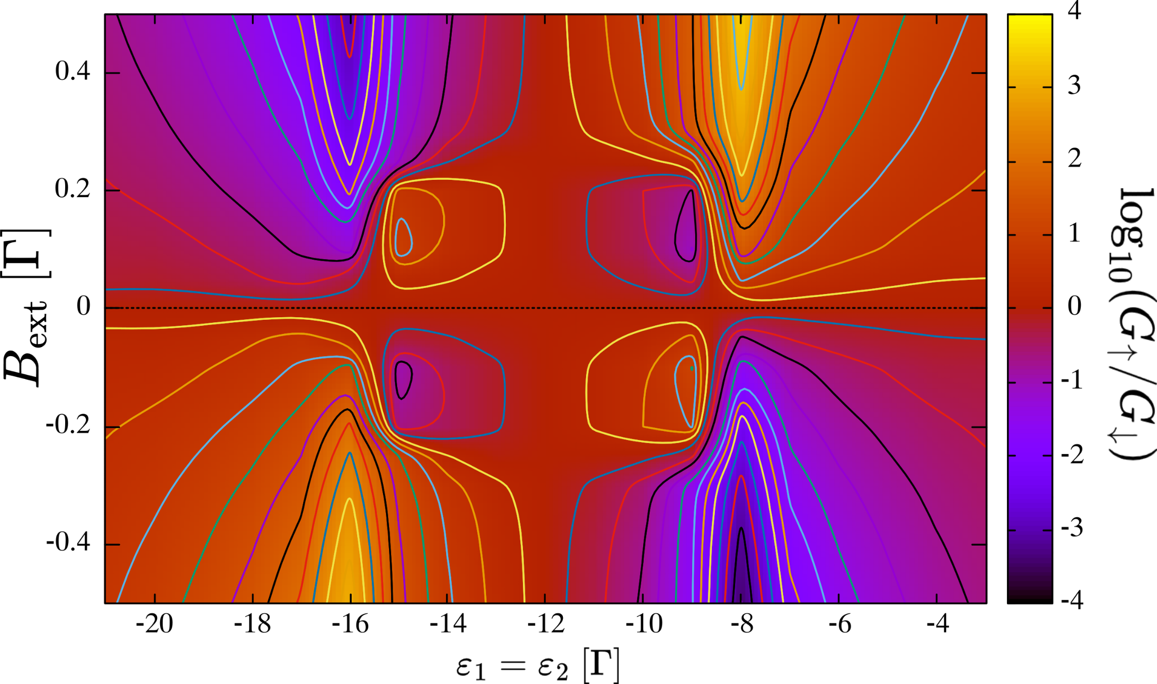
To give an overview of the possibilities of the device we present here, we show in Fig. 2 a diagram in which the logarithm of the ratio of spin-polarized conductances is plotted as a function of local energies and magnetic field . The temperature is low enough for the Kondo effect to play a crucial role in the transport properties, as will be explained later in this article. All parameters are in units. Coulomb interaction parameters are , and . In the diagram, goes from -21 to -3 and from -0.5 to 0.5. The parameter representing the inhomogeneity of the magnetic field at the sample surface is 10. The diagram shows four well-defined zones in which conductance is strongly spin-polarized. This polarization occurs when a magnetic field is applied to the device. Remarkably, the sign of gives direct information on the sign of , suggesting applications for direct imaging of antiferromagnetic surfaces. Indeed, alternative techniques such as single-spin magnetometer based on a single nitrogen–vacancy defect in diamond [10] require an additional external field to be applied in order to discriminate the sign of the measured field. Such a procedure, which could affect the measurement of the magnetic field emanating from the sample, is not necessary with the device we propose. Another important feature of the diagram in the figure 2 is the extremely high degree of spin polarization obtained. For well-tuned parameters, can reach . This property makes our device highly sensitive to the magnetic field emanating from the sample, but could also enable us to generate extremely pure spin-polarized currents. What is even more interesting is that the device can be switched from spin up filter to spin down filter very quickly by simply controlling the gate voltage , which could be very useful in spintronics for spin filtering.
In the following, we will see that the high sensitivity of the device is due to the Kondo effect, which induces a strong magnetic coupling between the spin states of dots 1 and 2. The existence of the Kondo effect under an applied magnetic field has been studied in many works, and it is well known that the magnetic field destroys the Kondo resonance through Zeeman splitting. In our device, this is not the case, as only dot 2 is immersed in a strong magnetic field, while dot 1 is exposed to only a weak magnetic field, allowing the Kondo effect to survive. In fact, as we will see below, the Kondo effect only persists for a unique spin species on the channel dot, implying a strong asymmetry between the conductances for each spin species.
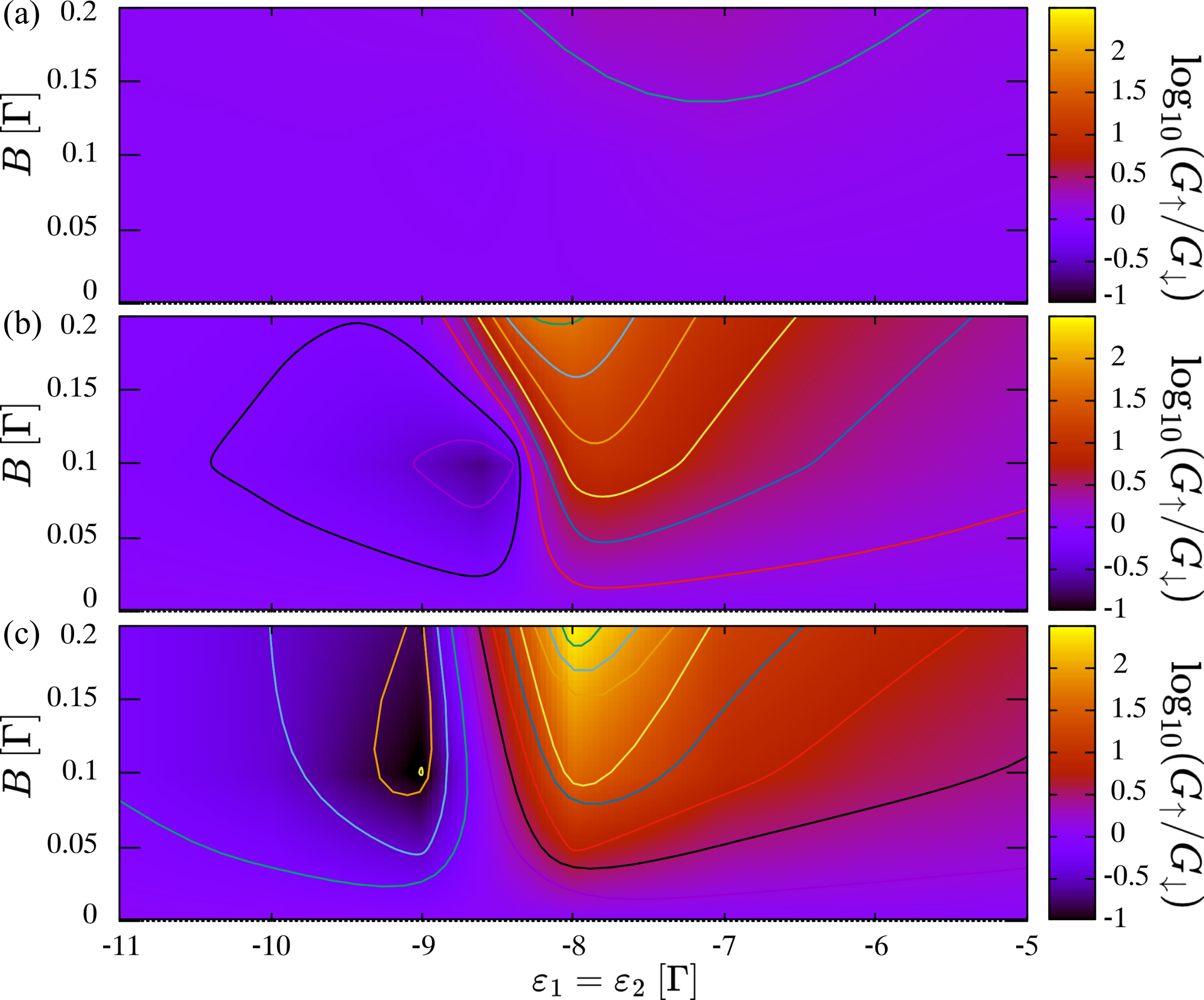
Transport through dot 1 is then highly affected by this magnetic effect, strongly differentiating the two electron spin states. Indeed, a first indication of the Kondo nature of transport is given in figure 3, where the ratio of spin-resolved conductances is plotted for different temperatures. In part (a) of the figure, the temperature is and even under optimum conditions, for (not shown), only reaches the value 0.15, i.e. . The device is very insensitive. Sensitivity increases sharply as the temperature is lowered, and for , significant values of are reached at moderate field strength .
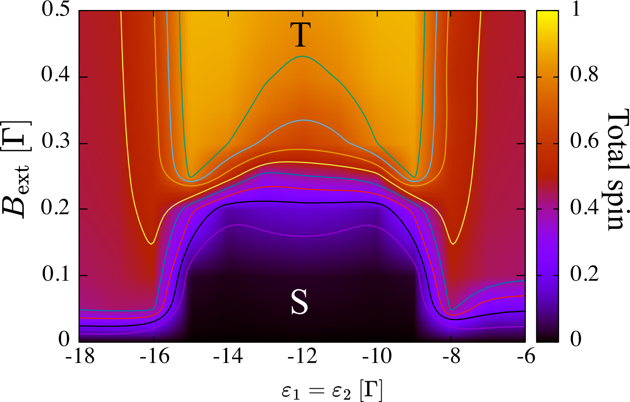
In order to better understand how the spin states of two dots can be coupled thanks to the exchange term of the Coulomb interaction between dots, we show in Fig. 4 how the total spin of the two-dot device evolves. Under magnetic field , dot 2 gets almost entirely polarized, parallel to the applied magnetic field. For site energies between -15 and -9, the polarization of dot 1 behaves differently depending on the value of the magnetic field. At high magnetic fields (above 0.2), dot 1 polarizes parallel to the applied field (as with dot 2), and the resulting total spin is 1 (zone T in Fig. 4). This two-dot state has strong similarities with a triplet spin state. The singlet state is obtained at lower magnetic fields (below 0.2). In this case, dot 1 polarizes antiparallel to the applied magnetic field. The spin of dot 1 is governed by antiferromagnetic inter-dot exchange coupling and Kondo physics. The resulting total spin is 0 (zone S in Fig. 4).
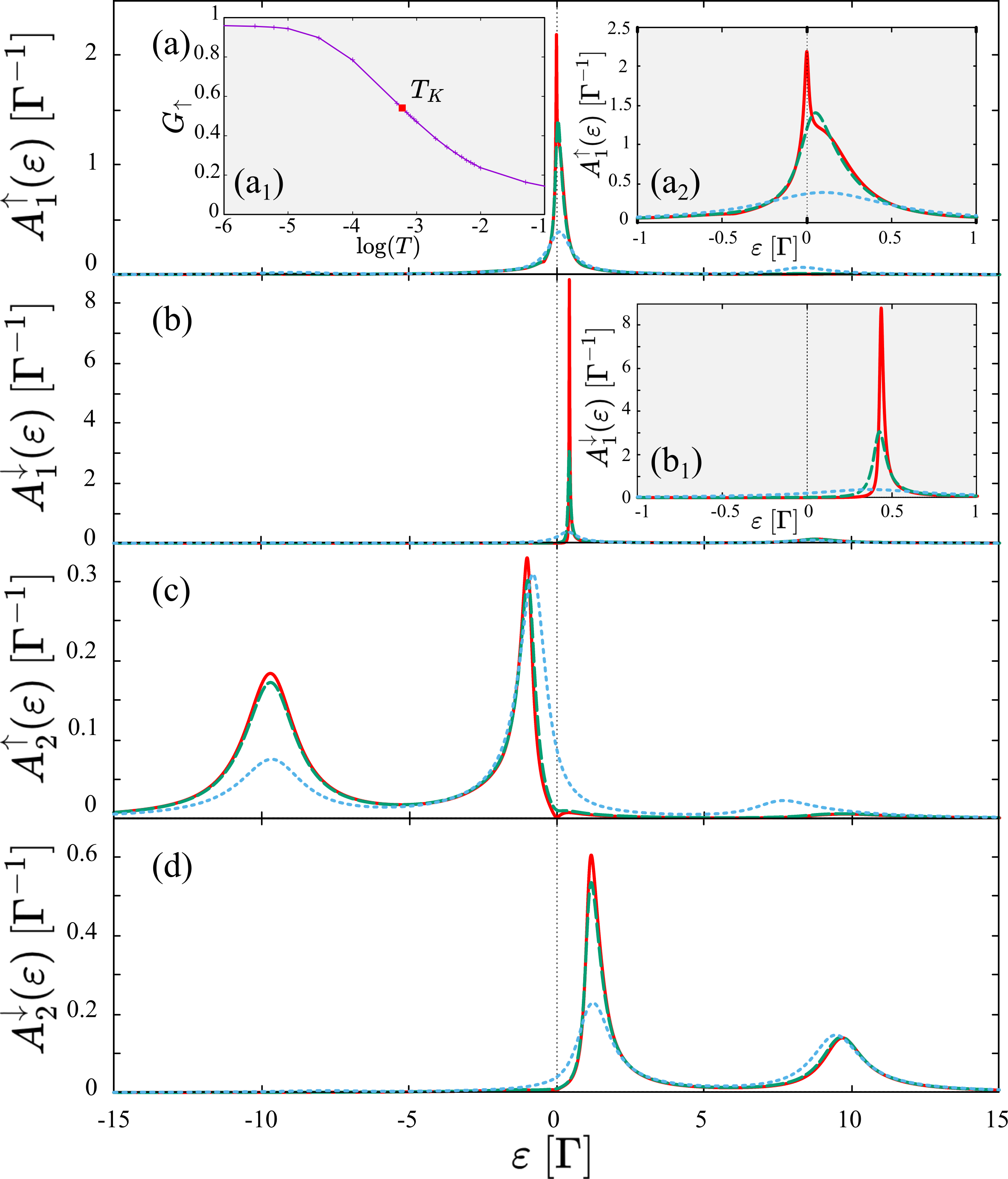
Finally, to gain a deeper understanding of how the Kondo effect impacts spin-resolved transport properties, we have plotted in Fig. 5 the spectral functions for each dot and spin, for the three temperatures , and . These results therefore give an indication of how the Kondo effect takes hold in the device. Indeed, inset (a1) shows the evolution of spin-up conductance as a function of temperature, enabling us to define the Kondo temperature for the chosen physical parameters . For dot 1, parts (a) and (b) of the figure show the spin-up and spin-down spectral functions for these three temperatures, respectively. Parts (c) and (d) relate to dot 2. Under a positive magnetic field (here ), the dot 2 spectral functions are strongly polarized by Zeeman splitting at all three temperatures explored. Temperature has only a slight effect at high energies, but greatly reduces the density of low-energy excitations, close to . In dot 1, the effect of temperature is much more pronounced, leading to strong discrimination between spins. The spectral function of the down spin is significantly lowered near , while that of the up spin is subject to a pronounced Kondo resonance at low temperature. The effect of this resonance is to boost the conductance of the up spin, which explains the significant increase in low-temperature sensitivity of the device described in this paper.
I Conclusion
In summary, we examined the electronic transport through a T-shaped double quantum dot with strong intra- and interdot Coulomb repulsions including exchange coupling and pair-hopping processes. In this setup, electrons may only flow from source to drain via the upper dot. The role of the lower dot is to monitor the upper dot spin-flow via an interdot interaction, depending on magnetic field on the lower dot. We have shown that the exchange interaction between dots enables the establishment of a Kondo regime at low temperatures. The device is then able to discriminate very selectively between the two spin states as a function of the applied magnetic field. We have shown that the selective development of an Abrikosov-Suhl-Kondo resonance for a unique spin species on the conduction dot makes it possible to achieve very large values of the spin conductance ratio. Potential applications in magnetic microscopy and spin filtering spintronics were discussed.
References
- [1] Coey, J. M. D. Noncollinear spin structures. Can. J. Phys. 65, 1210–1232 (1987).
- [2] Jungwirth, T., Marti, X., Wadley, P. and Wunderlich, J. Antiferromagnetic spintronics. Nature Nanotechnol. 11, 231–241 (2016)
- [3] M. P. Recher, E. V. Sukhorukov, and D. Loss, Phys. Rev. Lett. 85, 1962 (2000)
- [4] N. Sergueev, Qing-feng Sun, Hong Guo, B. G. Wang, and Jian Wang, Phys. Rev. B 65, 165303 (2002)
- [5] J. Fransson, E. Holmstrom̈, O. Eriksson, and I. Sandalov Phys. Rev. B 67, 205310 (2003)
- [6] M. Pustilnik and L. Borda, Phys. Rev. B 73, 201301R (2006)
- [7] R. Sánchez, E. Cota, R. Aguado, and G. Platero, Phys. Rev. B 74, 035326 (2006)
- [8] Winkler, R., Ciria, M., Ahmad, M., Plank, H., Marcuello, C. Nanomaterials 13, 2585 (2023) https://doi.org/10.3390/nano13182585
- [9] R Wiesendanger, M Bode, Solid State Communications, 119, 341 (2001) https://doi.org/10.1016/S0038-1098(01)00103-X.
- [10] Gross, I., Akhtar, W., Garcia, V. et al. , Nature 549, 252 (2017)
- [11] Ge, Z., Slizovskiy, S., Polizogopoulos, P. et al., Nat. Nanotechnol. 18, 250 (2023)
- Averin and Likharev [1986] D. V. Averin and K. K. Likharev, Journal of Low Temperature Physics 62, 345 (1986).
- Fulton and Dolan [1987] T. A. Fulton and G. J. Dolan, Phys. Rev. Lett. 59, 109 (1987).
- Lafarge et al. [1991] P. Lafarge, H. Pothier, E. R. Williams, D. Esteve, C. Urbina, and M. H. Devoret, Zeitschrift für Physik B Condensed Matter 85, 327 (1991).
- Kastner [1992] M. A. Kastner, Rev. Mod. Phys. 64, 849 (1992).
- Hewson [1993] A. C. Hewson, The Kondo Problem to Heavy Fermions (Cambridge University Press, Cambridge, England, 1993).
- Goldhaber-Gordon et al. [1998] D. Goldhaber-Gordon, H. Shtrikman, D. Mahalu, D. Abusch-Magder, U. Meirav, and M. A. Kastner, Nature 391, 156 (1998).
- Klein et al. [2007] L. J. Klein, D. E. Savage, and M. A. Eriksson, Appl. Phys. Lett. 90, 033103 (2007).
- Liang et al. [2002] W. Liang, M. Shores, M. Bockrath, J. Long, and H. Park, Nature 417, 725 (2002).
- Nygard et al. [2000] J. Nygard, D. H. Cobden, and P. E. Lindelof, Nature 408, 342 (2000).
- van der Wiel et al. [2000] W. van der Wiel, S. De Franceschi, T. Fujisawa, J. M. Elzerman, S. Tarucha, and L. P. Kouwenhoven, Science 289, 2105 (2000).
- Klochan et al. [2013] O. Klochan, A. P. Micolich, A. R. Hamilton, D. Reuter, A. D. Wieck, F. Reininghaus, M. Pletyukhov, and H. Schoeller, Phys. Rev. B 87, 201104 (2013).
- Daroca et al. [2018] D. P. Daroca, P. Roura-Bas, and A. A. Aligia, Phys. Rev. B 98, 245406 (2018).
- Mathew and Fang [2018] P. T. Mathew and F. Fang, Engineering 4, 760 (2018).
- Limburg et al. [2019] B. Limburg, J. O. Thomas, J. K. Sowa, K. Willick, J. Baugh, E. M. Gauger, G. A. D. Briggs, J. A. Mol, and H. L. Anderson, Nanoscale 11, 14820 (2019).
- Yu and Natelson [2004] L. H. Yu and D. Natelson, Nano Letters 4, 79 (2004).
- Wahl et al. [2004] P. Wahl, L. Diekhöner, M. A. Schneider, L. Vitali, G. Wittich, and K. Kern, Phys. Rev. Lett. 93, 176603 (2004).
- Tie et al. [2019] M. Tie, S. Gravelsins, M. Niewczas, and A. Dhirani, Nanoscale 11, 5395 (2019).
- [29] S. Smirnov and M. Grifoni, New Journal of Physics 15, 073047 (2022)
- [30] B. Danu, F. Assaad, and F. Mila, Phys. Rev. Lett. 123, 176601 (2019)
- [31] Zhang, Yh., Kahle, S., Herden, T. et al., Nat Commun 4, 2110 (2013)
- [32] C. Hsu, T. A. Costi, D. Vogel, C. Wegeberg, M. Mayor, H.S.J. van der Zant, and P. Gehring, Phys. Rev. Lett. 128, 147701 (2022)
- Chan et al. [2002] I. H. Chan, R. M. Westervelt, K. D. Maranowski, and A. C. Gossard, Appl. Phys. Lett. 80, 1818 (2002).
- Hübel et al. [2007] A. Hübel, J. Weis, W. Dietsche, and K. v. Klitzing, Appl. Phys. Lett. 91, 102101 (2007).
- Fringes et al. [2012] S. Fringes, C. Volk, B. Terrés, J. Dauber, S. Engels, S. Trellenkamp, and C. Stampfer, Phys. Status Solidi C 9, 169–174 (2012).
- Anderson [1961] P. W. Anderson, Phys. Rev. 124, 41 (1961).
- Maier et al. [2000] T. Maier, M. Jarrell, T. Pruschke, and J. Keller, Euro. Phys. J. B 13, 613 (2000).
- Otsuki and Kuramoto [2006] J. Otsuki and Y. Kuramoto, J. Phys. Soc. Jpn 75, 064707 (2006).
- Zamani et al. [2013] F. Zamani, T. Chowdhury, P. Ribeiro, K. Ingersent, and S. Kirchner, Phys. Status Solidi B 250, 547 (2013).
- [40] S. Yang, X. Wang, and S. Das Sarma, Phys. Rev. B 83, 161301(R) (2011)
- Jauho et al. [1994] A.-P. Jauho, N. S. Wingreen, and Y. Meir, Phys. Rev. B 50, 5528 (1994).
- Kim and Hershfield [2003] T.-S. Kim and S. Hershfield, Phys. Rev. B 67, 165313 (2003).
- Wingreen et al. [1993] N. S. Wingreen, A. P. Jauho, and Y. Meir, Phys. Rev. B 48, 8487 (1993).