Carrier Emission and Capture Competition mediated A(n)BC Recombination Model in Semiconductors with Multi-Level Defects
Abstract
The ABC model has been widely used to describe the carrier recombination rate, in which the rate of non-radiative recombination assisted by deep-level defects is assumed to depend linearly on excess carrier density , leading to a constant recombination coefficient A. However, for multi-level defects that are prevalent in semiconductors, we demonstrate here that the rate should depend nonlinearly on . When varies, the carrier capture and emission of defects can change the defect density distribution in different charge states, which can further change the carrier capture and emission rates of the defects and thus make the recombination rate depend non-linearly on , leading to an function. However, in many recent calculation studies on carrier recombination rate of multi-level defects, only carrier capture was considered while carrier emission from defect levels was neglected, causing incorrect charge-state distribution and misleading linear dependence of the rate on . For - in GaN and in CsPbI3, our calculations showed that neglecting the carrier emission can cause the recombination rate underestimation by more than 8 orders of magnitude when is cm-3. Our findings suggest that the recent studies on carrier recombination assisted by multi-level defects should be revisited with carrier emission considered, and the widely-used model should be reformed into the model.
I Introduction
Carrier recombination in semiconductors is an important process determining the performances of many semiconductor devices, such as the power dissipation of electronic devices [1, 2], quantum efficiency of light-emitting diodes [3], power conversion efficiency of solar cells [4], and responsivity of photodetectors [5]. In different semiconductors, the carrier recombination can be contributed by different mechanisms (or through different pathways), such as defect-assisted recombination, band-to-band recombination and Auger recombination [6, 7]. The recombination kinetics of these three mechanisms are usually described by the well-known ABC model, which claims the overall recombination rate [8, 9, 10, 11, 12, 13, 14, 15, 16], where is the carrier density, , and represent the monomolecular recombination coefficient (which is typically related to defect-assisted recombination [17]), bimolecular recombination coefficient (band-to-band recombination [6]), and trimolecular recombination coefficient (Auger recombination [8]), respectively.
In the model, defect-assisted recombination rate is assumed to have a linear dependence on carrier density. Therefore, the coefficient is considered as a constant independent of carrier density, which is widely accepted in the carrier dynamics characterization experiments, such as transient spectroscopy and time-resolved photoluminescence measurements [18, 19, 20]. In these measurements, a constant is extracted from the exponential fitting of the decay dynamics, for example, was measured to be constants of s-1 in InGaN [15], s-1 in CH3NH3PbI3 [21], and s-1 in GaAs [22]. Such a constant and the model are important for evaluating the contribution of different recombination mechanisms as well as manipulating carrier dynamics and lifetime in semiconductor devices. For example, the model shows that defect-assisted nonradiative recombination (the term) dominates at low carrier densities, band-to-band radiative recombination (the term) dominates at medium carrier densities, and Auger nonradiative recombination (the term) governs at high carrier densities, so the design of high-efficiency light-emitting diodes (LED) generally requires that the carrier density should be controlled at a medium level to promote the the radiative term and thus achieve the highest quantum efficiency / [23, 17, 24, 25]. Similar to the case in LED devices, the design of other devices also adopts the ABC model as a basic rule for the carrier dynamics manipulation [26, 8, 27, 28, 29].
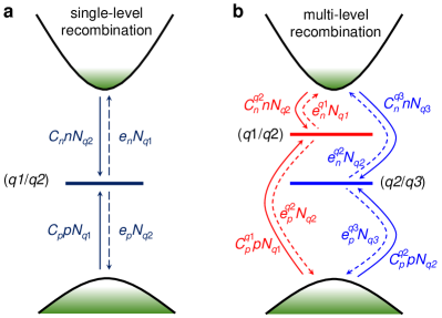
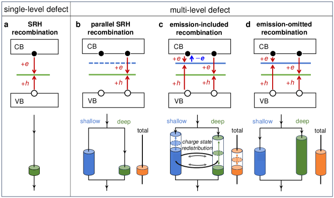
Actually, the linear dependence of defect-assisted recombination rate on carrier densities in the model can be traced back to the Shockley-Read-Hall (SRH) model [30, 31], as shown in Fig. 1(a). For a defect with a charge-state transition level in the band gap, there are four processes contributing to the overall carrier recombination: electron capture to the defect level, electron emission from the level, hole capture to and hole emission from the level. For instance, electron capture from CBM to the defect level can make the defect transit from to charge state. The corresponding electron capture rate can be expressed as , in which is the capture coefficient, is the electron carrier density, and is the defect density in state. Under continuous external injections or excitation of carriers, the four processes will reach a steady state when the net electron capture rate (capture rate offset by emission rate) equals to the net hole capture rate [32]. Consequently, as derived by Shockley, Read and Hall and introduced in many textbooks [30, 31, 33, 34], the defect-assisted recombination rate at steady-state can be expressed as,
| (1) |
where is the defect density, and are the electron and hole capture coefficients, respectively, and are the electron and hole carrier densities, is the intrinsic carrier density, and are the electron and hole densities when the Fermi level coincides with the defect level. According to Eq. (1), when the defect level is shallow, either or is extremely large, leading to a low value of . Only when the defect level is deep, can the defect have large . Therefore, it is well-known that deep-level defects are effective recombination centers [35, 36, 37]. For deep-level defects, and are very small and can be neglected, and usually in optoelectronic devices with high excess carrier density (, where , are equilibrium carrier densities, and is the excess carrier density), then the recombination rate can be simplified as [38, 39, 40]. Compared with the defect-assisted recombination () term in the model, we can find , which is indeed a constant. This is the reason why the linear dependence of defect-assisted recombination rate on carrier density as well as the model work well in dealing with the carrier recombination in deep-level defect systems [39, 41].
However, it should be noted that the derivation of SRH model was based on a single-level defect [42, 30, 31], so the SRH model should be in principle applicable only for defects with one single level in the band gap. Defects in real semiconductors usually produce two or more charge-state transition levels in the band gap, for instance, Si vacancy () defect produces three levels in the 1.17 eV band gap of Si (at 0.38 eV for , 0.63 eV for , and 1.0 eV for charge state transition) [43], in GaN [44] and in CH3NH3PbI3 [45] each produces two levels. Each charge-state transition level of such defects can cause carrier capture and emission, determining the overall defect-assisted recombination rate collectively. For multi-level defects, whether the recombination rate still has a linear dependence on carrier densities remains unclear.
Given the prevalence of multi-level defects in semiconductors, accurately calculating the recombination rate in multi-level defect systems has been a long-standing research topic over the past 60 years [46, 47, 48]. In 2016, Alkauskas et al. studied the recombination in a three-level defect system and defined a total capture coefficient to calculate its recombination rate [38]. In the following years, has been extensively adopted to calculate the recombination rate in multi-level-defect systems [49, 50, 51, 52, 53, 54, 55, 56, 57]. For a two-level defect, which has three charge states , and , was derived as [49, 50, 51, 52, 53, 54, 55, 56, 57],
| (2) |
where and are the electron and hole capture coefficients of transition level, and are the electron and hole capture coefficients of transition level. The corresponding recombination rate . In the derivation of Eq. (2), the carrier capture processes at ( and transition levels were considered, while the corresponding carrier emission processes were neglected. Therefore, the carrier capture rate at each level is directly regarded as the net carrier capture rate, neglecting the contribution of the carrier emission rate. According to Eq. (2), is obviously a constant independent of carrier density. Thus, the coefficient () in the model is also a constant, which indicates that the recombination rate for multi-level defect also has a linear dependence on carrier density.
However, in this work we will show the coefficient is actually NOT a constant in semiconductors with multi-level defects. The competition between carrier capture and carrier emission processes influences the distribution of defect density in different charge states and thus the overall recombination rate significantly. Since the competition varies with excess carrier densities, the coefficient changes quickly as a function of the carrier density , rather than being a constant. In recent calculation studies based on formula, neglecting the carrier emission from defect levels make the defects act only as carrier trapping centers and stay ineffective for carrier recombination, therefore, the carrier recombination rates can be severely underestimated by orders of magnitude and the coefficient behaves as a constant erroneously. Our results indicate that when multi-level defects exist, a more rigorous formula considering both the carrier capture and emission of all defect levels should be used for calculating the recombination rate , and the well-known model should be reformed into the model in carrier dynamics manipulation.
II Results
II.1 Sah-Shockley recombination model of multi-level defects
The carrier recombination assisted by multi-level defect has been rigorously studied by Sah and Shockley in 1958 [46], where the derivation of recombination rate included both carrier capture and emission. Unfortunately, recent studies followed the rate equation of single deep-level defect and neglected carrier emission contribution, deriving the simplified formula of a total capture coefficient , e.g., Eq. (2) [49, 50, 51, 52, 53, 54, 55, 56, 57]. Here, to demonstrate the importance of carrier emission, and show the difference of recombination assisted by single-level and multi-level defects, we follow the derivation of Sah and Shockley and introduce the recombination rate formula first.
In multi-level defect systems, the carrier capture and emission processes may occur individually at different levels, complicating the overall recombination process. For simplicity, we illustrate in Fig. 1(b) by a two-level defect with three charge states , , , where the charge-state transition level is close to the conduction band minimum (CBM) while the level is located deeply in the band gap. There are totally 8 capture and emission processes at two levels, which collaboratively determine the overall recombination rate. The capture and emission rates have been indicated in Fig. 1(b). For carrier emission, the rate constant () can be expressed as () or (), where and are the electron and hole densities when the Fermi level coincides with the defect level, and and are those when the Fermi level coincides with the defect level. Under steady-state condition, the net electron capture rate should be equal to the net hole capture rate for each level,
| (3) |
| (4) |
where and are the electron and hole capture coefficients of level, and and are those of level. Combining the condition that the total defect density should be equal to the defect density in all the three charge states, , with Eqs. (3, 4), the defect density in each charge state under the steady-state condition can be expressed as,
| (5) |
| (6) |
| (7) |
where . Consequently, the recombination rate can be written as [46] (the detailed derivations and the extension to arbitrary number of defect levels are given in Supplemental Material [58, 59, 60]),
| (8) |
Following the definition of [7], the multi-level defect-assisted recombination coefficient can be defined as,
| (9) |
Since the carrier emission has been included in the derivation, we denote it as emission-included recombination (EIR). If the carrier emission is completely neglected, the rate of emission-omitted recombination (EOR) can be simplified from Eq. (8) as,
| (10) |
The coefficient can also be defined as , similar to Eq. (9). Note that if a condition of is supposed, Eq. (10) can be further simplified to “” formula proposed by Alkauskas et al., that is, , where is given in Eq. (2). Below we will take an example to show the difference between and , and illustrate that is actually not a constant in nonradiative recombination assisted by multi-level defects.
II.2 Carrier emission contribution to recombination rate
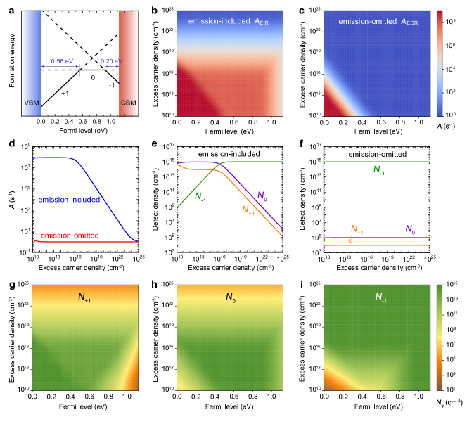
We use a two-level defect in a semiconductor with 1.12 eV band gap as an example. The defect introduces two charge-state transition levels in the band gap, and , as shown in Fig. 2(a). The relatively shallower level is 0.2 eV below the CBM, and the deep level is located at 0.56 eV above the VBM, corresponding to the and transition levels shown in Fig. 1(b). Such defects are common in semiconductors and similar to impurities in silicon, such as Au and Pt [61, 62]. The capture coefficients and at level are cm3 s-1 and cm3 s-1, and at level are cm3 s-1 and cm3 s-1, respectively. These coefficients follow the general trend in the nonradiative multiphonon theory that the nonradiative capture rate increases exponentially as the electronic transition energy between the initial and final states decreases [63, 64, 65, 66]. The total defect density is assumed to be cm-3. The defect densities distributed in the three charge states as well as the overall recombination rates can be calculated following Eqs. (3-10) where , , and are referred as , , and , respectively.
Fig. 2(b, c) show the heat maps of calculated coefficients as functions of excess carrier density and equilibrium Fermi level when the carrier emission contribution is included and omitted, respectively. As shifts from the left side (VBM) to right side (CBM), the electrical conductivity changes from -type to intrinsic, and then to -type. From the heat map, we can see that including the carrier emission contribution has very large influence on the coefficients, i.e., the emission-included is larger than the emission-omitted in most areas of the map. Below we will introduce the differences in detail and analyze their physical origins.
When the equilibrium Fermi level is located at the middle of the band gap (corresponding to ), we plot in Fig. 2(d) the variation of coefficients with excess carrier density. According to , Eq. (10) where , and Eq. (2), we can derive that , so is almost independent of excess carrier densities, explaining the nearly constant straight line of in Fig. 2(d). Considering the values of , , and , it is easy to understand that the calculated is very low (on the order of s-1). Therefore, such a defect is not an effective recombination center when the carrier emission is omitted. In contrast, exhibits a strong dependence on excess carrier density, i.e., it changes by 7-8 orders of magnitude as the excess carrier density increases in Fig. 2(d). When carrier density is in the range 1010-1016 cm-3, can be as large as 108 s-1, indicating the defect can be a very effective recombination center, which contradicts the conclusion obtained from when carrier emission is omitted. Only when the excess carrier density is extremely high ( cm-3), can be close to . These results indicate that the and coefficients may differ by 7-8 orders of magnitude for solar cell (usually 1015 cm-3) [6] and 5-6 orders of magnitude for light-emitting diode (usually 1018 cm-3) applications [25].
To reveal the origin of the large discrepancy between and , we show in Fig. 2(e, f) the defect densities distributed in , (neutral), charge states. When the emission effect is included in the calculation, the densities in the and charge states keep almost unchanged at a high value around 1015 cm-3 (almost all the defects are in these two charges states) when is low, but decrease rapidly to a very low value when is high, as shown in Fig. 2(e). Such a trend is quite similar to that of the emission-included in Fig. 2(d), indicating that the recombination coefficient is positively and strongly correlated with the defects in the and charge states. The defect density in the charge state show an opposite trend to those of the and charge states. When the carrier emission is omitted, the density distribution become completely different, and almost all the defects take the charge state, as shown in Fig. 2(f). The densities of all the three charge states are constants independent of the carrier density, in accordance with the constant in Fig. 2(d), further indicating that the recombination coefficient of the two-level defect is strongly correlated with its density distribution in different charge states.
Now we will analyze how the charge-state distribution of defects are correlated with the carrier emission and recombination coefficient. As shown in Fig. 2(a), there are two charge state transition levels, and , in the band gap. The transition level is high and close to CBM. Therefore, the transition energy of the electron capture from CBM to level is small and thus the electron capture coefficient is large, while the transition energy of the hole capture from VBM to level is large and thus the hole capture coefficient is very small [67]. Correspondingly, is large and is small. According to Eq. (1), the single level has a very small recombination coefficient and thus cannot assist the electron-hole recombination effectively. In contrast, the transition level is deep in the middle of the band gap, so its electron and hole capture coefficients, and , both have medium values, and both and are not very large. Therefore, the single deep level can have a large recombination coefficient, in accordance with the common expectation that the deep-level defects are effective recombination centers in the SRH theory. Since only the deep level can assist electron-hole recombination effectively while the level cannot, we can understand why the strong and positive correlation between the recombination coefficient in Fig. 2(d) and the and charged defect densities in Fig. 2(e), because the and charged defects can be involved directly in electron-hole recombination. The charge defects cannot be involved in the recombination directly, and can only be involved after it emits an electron or captures a hole and then transits back into the neutral state. Therefore, the coefficient in Fig. 2(d) is inversely correlated with the charged defect density in Fig. 2(e).
As we can see, the neutral state can participate in both the and transitions, so it is special in the three states and can mediate the carrier capture and emission rates of the two levels, making the two levels influence each other during the electron-hole recombination. The influence gives rise to the obvious changes of the defect charge state distribution in Fig. 2(e) and the changes of recombination coefficient in Fig. 2(d). As the excess carrier excitation or injection reaches a steady state, the electron and hole capture/emission at the shallower level satisfy Eq. (3), thus
| (11) |
which means that the summed transition rate (electron capture plus hole emission) from neutral to charged state equals that (hole capture plus electron emission) from charged to neutral state. Since is much smaller than , and is smaller than , the hole capture and hole emission rates can be reasonably neglected, giving . Hence, the electron capture rate and its counteracting electron emission rate are dominant in Eq. (11). When the excess carrier density is low (thus is low), is much smaller than , then Eq. (11) requires the neutral defect density to be much higher than the charged defect density . The high density of neutral defects leads to high recombination coefficient through the deep level. When the excess carrier density increases to a high level (thus is high), becomes comparable to or even higher than , then has to decrease to be comparable to or lower than . The decrease of further causes the decrease of the recombination coefficient . Based on such a competition between the electron capture and emission rate associated with the level, we can explain the decrease of in Fig. 2(e) and in Fig. 2(d).
If the carrier emission effect is omitted in the calculation, as shown in Eq. (10) and reported in the calculations based on the formula, the competition disappears completely, then Eq. (11) cannot be satisfied. Since the capture rate of level is high, the defects capture electrons quickly, transits into the charge states and cannot transit back to the neutral state any more. That makes almost all the defects take the charge state, giving a high and constant and very low and independent of excess carrier density in Fig. 2(f). The constant and low density of neutral and charged defects makes the recombination coefficient also lose its dependence on excess carrier densities and much lower than in Fig. 2(d).
Taking the intrinsic system with a middle-gap Fermi level () as an example, the analysis above shows in detail how omitting the carrier emission effect in the calculation causes the incorrect defect charge-state distribution and thus the seriously underestimated recombination coefficient . Besides, for -type or -type system where the Fermi level approaches CBM or VBM, omitting carrier emission also causes large difference in the calculated coefficients and . The corresponding distribution of defect densities with emission included are shown in Fig. 2(g-i), while those with emission omitted are shown in Fig. S1 in Supplemental Material. We can also see that the very different and are correlated with the large differences in defect-density distribution. Detailed analyses are presented in Supplemental Material.
According to a series of recent first-principles calculations based on the formula that omitted the carrier emission, the multi-level defects with both shallow and deep levels are mostly stuck at one charge state associated only to the shallow level. This is because the shallow level typically has a high capture rate for one type of carriers, while has a very low capture rate for the other type of carriers. Since the overall electron-hole recombination rate is limited by the lower rate, the slower carrier capture process is denoted as a “rate-limiting” step in previous studies [59, 39]. For example, in our example shown above, omitting carrier emission shows most defects are stuck at charge state, so the slow hole capture process at level acts as the “rate-limiting” step, which erroneously deactivates this defect in the overall recombination process. However, when carrier emission is included, we find it is exactly the carrier emission from the shallower level that reactivates the defects from charge state to the neutral state and then assists the electron-hole recombination through the deep level. Therefore, our results show that the carrier emission from the shallower level can be regarded as an important “rate-reactivating” step, rather than a “rate-limiting” step.
It should be noted that if the recombination at shallow level is more efficient than that at deep level, probably caused by different phonon frequencies or anharmonicity during multiphonon transition, considering carrier emission would retard the overall recombination. In such a rare scenario, can be lower than when carrier density is low.
II.3 Strict conditions required for omitting carrier emission
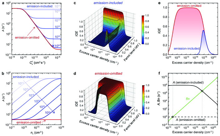
Given the emission rate constant has a form as , to figure out the condition when carrier emission can be reasonably omitted, we investigate the variation of coefficients with electron capture coefficient in Fig. 3(a), and the variation of coefficients with (determined by the energy difference between the defect level and CBM level) in Fig. 3(b). In Fig. 3(a), we gradually increase the electron capture coefficient and meanwhile fix the level at a shallow location, 0.2 eV below CBM. When is very small, the carrier emission can be omitted because and are almost equal. As increases, the differences between and are widened due to the enhanced carrier emission effect of level. The blue lines show with varied excess carrier densities . When is low, e.g., 1014 cm-3, is much larger than , so the defects are mostly in the neutral state according to Eq. (11) and can give a high recombination rate through the deep level, and thus, is a large constant at 108 s-1 with varied . For a higher , decreases as increases. Only when ∆n is as high as 1024 cm-3, the and lines overlap in the most range of , indicating that the carrier emission can be neglected under a such high excess carrier density.
In Fig. 3(b), the electron capture coefficient is fixed but varies from 1011 cm-3 to 1019 cm-3, i.e., the level shifts upward from a deep middle-gap location to a shallower location near CBM. The calculated is a constant independent of and the level, in accordance to Eq. (10). However, because of the competition between and , has a strong dependence on both the location of the level in the band gap and the carrier density. The difference between and is widened when the level becomes shallower ( increases) and the excess carrier density decreases. Only when is higher than by 9-10 orders of magnitude, can and lines overlap. That means, either has to been very low or has to be very high. Since of a shallow level is usually higher than 1015 cm-3, has to be higher than 1024 cm-3.
Based on these analyses, in the calculation of the recombination coefficient of multi-level defects, omitting the carrier emission can be acceptable only if one of the three conditions are satisfied: (i) the excess carrier density is very high, almost 1024 cm-3. It should be noted that such a high carrier density is beyond the common carrier density in optoelectronic devices, so this strict condition is meaningless for studies of functional semiconductors; (ii) the shallow level of the defect has a very small (for shallow levels near CBM) or (for shallow levels near VBM). This condition is also not easy to be satisfied, because the small energy difference between the shallow level and the band edge usually leads to a large carrier capture coefficient according to the multiphonon theory; (iii) All levels of the defect are deep (far from the band edge), so even the shallowest level has a very low or , e.g., lower than 1010 cm-3. Since the first and second conditions are both too strict to be satisfied and only the third condition is possible, omitting the carrier emission can cause large errors in the calculated recombination coefficient if one of multiple defect levels is shallow.
II.4 A(n)BC recombination model and quantum efficiency calculation
The section above shows clearly that the multi-level defect assisted recombination coefficient is a function of carrier density, , when both the carrier capture and emission are considered. Therefore, the defect-assisted recombination coefficient in the recombination model should also be replaced by the function, then the model becomes . In this sense, it becomes questionable to attribute simply the first-order term to the defect-assisted recombination, the second-order term to the band-to-band recombination and the third-order term to the Auger recombination, because the multi-level defect-assisted recombination rate is not exactly first-order. Neglecting the carrier emission will cause a constant coefficient () and first-order dependence of the rate on carrier density, which will cause large errors in the calculated total recombination rate. The errors can further cause large errors in the calculation of the internal quantum efficiency (IQE), which is the ratio of radiative recombination rate in total recombination rate [8],
| (12) |
where is the first term of the denominator. IQE is an important quantity for assessing the optoelectronic performance of light-emitting and photovoltaic semiconductors, so the calculation errors can cause serious problems in the design of LED and solar cell devices.
To show how large errors the omission of carrier emission and the constant coefficient can cause in the calculation of IQE, we calculate in Fig. 3(c, d) the variation of IQE with excess carrier density and equilibrium Fermi level. IQE in Fig. 3(c) is calculated based on the carrier emission included , and that in Fig. 3(d) is calculated based on the carrier emission omitted . The radiative recombination coefficient ( coefficient) is assumed to be 10-11 cm3 s-1, and Auger recombination coefficient ( coefficient) is assumed to be 10-29 cm6 s-1 (typical values for semiconductors) [7]. Comparing Fig. 3(c) and Fig. 3(d), it is obvious that neglecting the carrier emission underestimates the coefficient and thus overestimates the IQE significantly in most areas.
This can be seen more clearly in Fig. 3(e) which shows the IQE with the Fermi level fixed at the middle of the band gap. The emission-omitted IQE (red curve) is much higher than the emission-included IQE (blue curve). In the region with the excess carrier density 1012-1016 cm-3, the red curve shows a wide peak with almost 100% efficiency, while the blue curve shows almost no efficiency. Only when the excess carrier density is around 1018 cm-3, the blue curve shows an efficiency peak of only 50%. The large difference of IQE results from the difference between and , which changes the competition between the non-radiative recombination term and the radiative recombination term in Eq. (12). As shown in Fig. 3(f), is a small constant and becomes much smaller than when excess carrier density is higher than 1012 cm-3, leading to the very high IQE in Fig. 3(e). In contrast, the non-radiative term is much larger than the term, suppressing IQE to almost 0 when the excess carrier density is lower than 1016 cm-3. As the density further increases, decreases and becomes smaller than the term when the density is higher than cm-3, then IQE increases to a higher level.
The comparison shows clearly that the small and constant coefficient caused by neglecting carrier emission effect can cause large errors in the IQE calculation based on the recombination model. Not only the peak efficiency, but also the curve shape of the IQE dependence on the excess carrier density and Fermi level, can have large errors if the carrier emission effect is not considered. Such kind of errors and the dependence of coefficient on excess carrier density in the model should be paid special attention to in the computational design of various optoelectronic devices based on semiconductors with multi-level defects.
II.5 Revisiting recent calculations based on formula
The discussion above demonstrated that carrier emission plays a critical role in determining the distribution of defect densities in different charge states and thus the overall recombination rate induced by multi-level defects, however, the role is neglected in the recent calculations based on the total capture coefficient formula which was firstly proposed in 2016 [38]. We noticed that dozens of recent studies have adopted this formula to analyze the recombination statistics of multi-level defects in materials, and obtained coefficients that are independent of carrier densities [49, 50, 51, 52, 53, 54, 55, 56, 57]. Here we start from the original data in Ref. [38] and recalculate the recombination coefficients to show that the direct use of the formula with no carrier emission effect may cause serious underestimations of coefficients and the defect-assisted non-radiative combination rate.
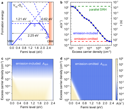
The defect configuration studied in Ref. [38] is a vacancy-substitution complex (-) in InGaN alloy ( = 2.42 eV), which has three charge-state transition levels, , , and levels, as plotted in Fig. 4(a). We reproduce capture coefficients (Table S1) using Nonrad code [68] based on the parameters given in Ref. [38] to be fully consistent with their calculation, and show the related configuration coordinate diagrams in Fig. S2 and Fig. S3 of Supplemental Material [58]. If the formula is simply adopted, the corresponding coefficient is only s-1 (assuming defect density as cm-3), which indicates - is not an effective recombination defect in InGaN, consistent with the conclusion of Ref. [38] that the complex in the ground state cannot act as a recombination center. However, it should be noted that both the and levels are very close to the CBM, so the carrier emission from these two levels cannot be neglected according to our previous analysis.
Fig. 4(b) shows the calculated of InGaN when (equilibrium Fermi level is at the middle of the band gap). When the excess carrier density is not very high, the electron emission rate (emission from level) and (emission from level) are both non-negligible. The strong carrier emission increases the defect density in neutral state in a transition path , in stark contrast to the claim in Ref. [38] that almost all the defects stay in and charge states, as shown in the comparison in Fig. S4. With the high density of neutral defects, the quick electron-hole recombination through the deep level makes the coefficient as high as s-1 at low . However, the value of is lower than s-1, indicating a huge error caused by omitting the carrier emission. It is also reported in Ref. [38] that the slow hole capture process at shallow level acts as a “rate-limiting” step that retards the overall nonradiative recombination. Our results here show clearly that its large electron emission rate prevents the overall recombination rate from being limited by the “rate-limiting” step, because the quick electron emission makes most defects transit back to the neutral state.
When increases, the competition between emission rate and capture rate at both and levels changes the distribution of the defect densities in different charge states, that is, - transits from and charge states to charge state gradually. Then the density decrease of neutral defects and the density increase of and charged defects cause the decrease of coefficient as increases, as shown by the blue line in Fig. 2(b), because the role of slow recombination through the shallow and levels becomes increasingly important. Comparing the declining blue line (emission included) and the constant red line (emission omitted) line, we can see that the error of the calculated coefficient is reduced from 13 orders of magnitude to 0 as increases. Under extremely high over cm-3, the electron capture at level prevails over the electron emission overwhelmingly, resulting in a much higher density of charged defects. Then the slow hole capture process of shallow level becomes the rate-limiting step, similar to the results calculated without emission [38], so the error in also disappears.
Fig. 4(c, d) show the heat map of coefficients as functions of equilibrium Fermi level (as the Fermi level shifts from left to right, the conductivity changes from -type to intrinsic and -type) and excess carrier densities in InGaN. When Fermi level ranges from about 0.6 eV above the VBM to the CBM, the calculated remains unchanged against the increase of and is as small as s-1, but within this Fermi level range undergoes a gradual decrease with the increase of . In strong -type condition with Fermi level below 0.5 eV, both and are large when cm-3, because most defects stay in charge state in both methods and thus the rapid recombination at level facilitates the overall recombination. Nevertheless, the coefficient causes non-negligible errors if the carrier emission is omitted regardless of the equilibrium Fermi level position.
In Ref. [38], the omission of carrier emission causes the small coefficient and slow recombination rate, so that an efficient recombination cycle would not be accomplished if only the ground state of - is considered, and the authors resorted to the assistance of excited state for explaining the fast recombination. After revisiting the process with carrier emission considered, we find the coefficient of the ground-state - can also be large, so its role in recombination should not be neglected. Similar effects of carrier emission may also exist in the recombination assisted by excited states.
In another example, carrier recombination at in halide perovskite CsPbI3, our study shows omitting the carrier emission also underestimates the coefficient by orders of magnitude. In Ref. [59], the antisite was shown to have and transition levels. Using the formula, it has been shown in Ref. [59] that it is the slow hole capture at shallow (+1/+2) level with a capture coefficient smaller than cm3 s-1 that limits the overall recombination rate. As a result, the emission-omitted total capture coefficient was found to be very small, arriving at the conclusion that cannot act as a recombination center. However, the level lies just 0.33 eV below CBM, so the carrier emission from the level should play a role in the nonradiative recombination. To make a comparison of capture coefficients, an emission-included total capture coefficient can be defined,
| (13) |
In Fig. 5(a), we compare our calculated (at cm-3) and (independent of ) calculated in Ref. [59]. As we see, the difference can be as large as 10 orders of magnitude. If the defect density is assumed to be cm-3, we calculate with different excess carrier densities and in Fig. 5(b). When reaches an extremely high (but not reasonable) value of cm-3, decreases to a lower limit and becomes comparable to , and the corresponding coincides with of cm3 s-1 reported in Ref. [59].
In Fig. 5(c), we plot the ratio of / (equals /) at different excess carrier densities and Fermi levels. The large values of the ratio show are much larger than in the whole range of Fermi level. The difference between and is very large when is low and becomes relatively smaller as increases. However, even at an extremely high ∆n of cm-3, the difference between and can still be as large as 3 orders of magnitude. Since does not change with , the change of / ratio originates mainly from the variation of with , which is determined by the densities of in +2 charge state. As shown in Fig. 5(d), when carrier emission is considered, the defect density in +2 charge state significantly increases when decreases, so is relatively large at low but gradually decreases with the increase of . According to our calculation, when is on the order of cm-3 at 300 K, is about s-1 when defect density is assumed to be cm-3. This value increases to s-1 if we a assume a higher defect density of cm-3, indicating that may act as an effective recombination center in CsPbI3. However, if the carrier emission is omitted in the calculation, is only about s-1 and s-1 at defect density of cm-3 and cm-3 respectively, indicating that can be excluded as a recombination center. Therefore, omitting carrier emission causes an incorrect conclusion about the role of in nonradiative recombination.
II.6 Parallel-circuit recombination model of multi-level defects
For a semiconductor with multiple types of single-level defects, the total recombination rate is sum of the SRH recombination rates of all types of defects. Correspondingly, the total carrier lifetime can be written as,
| (14) |
where , and are the carrier lifetime in the semiconductor with only one type of single-level defects. This relation can be analogized to the total resistance of multiple resistors in parallel, where the lifetime τ is analogized to the resistance and the recombination coefficient is analogized to the electric current (Note for the SRH recombination assisted by a single-level defect). The resistor analogue of a single-level defect is schematically shown in Fig. 6(a). The two-resistor parallel-circuit analogue of two single-level defects is schematically shown in Fig. 6(b).
For multi-level defects, if we assume each defect level assists the SRH recombination of conduction-band electrons and valence-band holes independently and do not influence each other, then the multi-level defect can be approximated as equivalent to multiple independent single-level defects. We call this approximation as the parallel SRH (PSRH) recombination model of multi-level defects. For example, we can approximate the two-level defect in Fig. 2(a) as equivalent to two single-level defects, as plotted in Fig. 6(b). The first single-level defect with the shallow level can be taken as a long resistor because the recombination coefficient through the level is low and the corresponding lifetime is long, and the second single-level defect with the deep level can be taken as a short resistor because the recombination coefficient through the level is high and the corresponding lifetime is short. Then, similar to the total resistance of resistors in parallel, the total lifetime is short as determined mainly by the short . In other words, since is much longer than , the influence of the shallow level can be neglected. Based on this approximation, several recent studies [69, 70, 71] on multi-level defects considered only the deep level of the defect and neglected the shallow level when calculating the carrier recombination coefficient and lifetime.
Approximating a multi-level defect to multiple independent single-level defects is also commonly adopted in semiconductor device modeling software, such as the well-known Sentaurus and Silvaco TCAD [72]. However, as we mentioned, the recombination model with a constant coefficient is valid for single-level defects, so the PSRH approximation, which takes the sum of coefficients of single-level defects as of a multi-level defect, will cause an incorrect conclusion that of a multi-level defect is also a constant independent of excess carrier density, in contrast with the model. Now we will analyze why the PSRH approximation causes errors in the calculated recombination coefficient and thus causes the incorrect conclusion.
Using the PSRH approximation, we calculated and the corresponding for - in InGaN, and found that and do not change with , as shown by the flat line in Fig. 4(b). In a wide range of , is much lower higher than . Therefore, neglecting the influence of shallow level in the PSRH approximation causes large errors in the calculated recombination coefficient and lifetime . Comparing , and in Fig. 4(b), we can find that decreases from to as increases, i.e., is the upper limit of at low , while is the lower limit of at high . That indicates the origin of the error in the calculated should be different from that in .
To understand the origin, we propose a modified parallel-circuit recombination model that includes the carrier emission effect (Fig. 6(c)) and a model that omits the carrier emission effect (Fig. 6(d)). Compared to the PSRH approximation in Fig. 6(b) that takes a multi-level defect as equivalent to multiple single-level defects, the major modification in the emission-included parallel-circuit recombination model is that the lifetimes and of the two assumed single-level defects are not constants, and they are correlated with each other and can change with . In contrast, and of two single-level defects in the PSRH approximation are constants and not influenced by other each other, which further makes the total lifetime () a constant. The necessity of the modification results from the defect charge state redistribution with varied excess carrier density when the carrier emission effect is included. As proved in Supplemental Material, the total carrier recombination rate assisted by multi-level defect can be expressed as the sum of recombination rate through each defect level, so the total lifetime can indeed be described by Eq. (14). However, the recombination coefficients and lifetimes of each defect level should depend strongly on the defect densities in each charge state, which varies sensitively with due to the competition between carrier capture and carrier emission, as analyzed in Section 2. For example, and of the shallow level and and of the deep level in Fig. 6(c) should all vary with , which further makes the total lifetime vary with , so the length of two parallel resistors and the length of total resistor are all variable. Since the total density of the defect in all three charge states is fixed, the recombination coefficients ( and ) and lifetimes ( and ) of two defect levels are correlated with each other, rather than being independent.
In the PSRH approximation, since the SRH recombination through the two assumed single-level defects are independent of each other and the density of each single-level defect is assumed the same as the density of the original two-level defects, the and defect-charge-state-distribution mediated correlation between and (similarly for and ) disappears. Since the density of the single-level defect with the deep level is fixed at a high value, all the defects are assumed to take the and charge states, which will cause rapid recombination through the deep level and give a large constant and thus a small . Therefore, the total lifetime () calculated using PSRH approximation is also a constant and underestimated (as shown by the short resistor in Fig. 6(b)) seriously by the incorrect defect density assumption. According to this, we can also understand why is the upper limit of at low in Fig. 4(b), because most of the defects indeed take the and charge states at low . As increases, more defects transit into the state, so the error caused by PSRH approximation increases. Such errors should be paid special attention to when one or several shallow levels of a multi-level defect is neglected in the carrier dynamics calculation.
For the emission-omitted parallel-circuit recombination model in Fig. 6(d), and (similarly for and ) are also constants independent of and not correlated with each other. Omitting carrier emission means no competition between carrier capture and carrier emission, so the defect densities in different charge states are constants independent of as shown in Fig. 2(f), which makes and constants independent of . Meanwhile, since omitting carrier emission make most of the defects stuck in the state and the densities of and charged defects are very low, of the level becomes much longer. Then both and are long, so is also long and the corresponding is small, explaining why is the lower limit of at high in Fig. 4(b).
III Conclusions
In summary, we find the carrier emission effect plays important roles in multi-level defect assisted recombination and cannot be neglected in the calculation of recombination rates. Neglecting the effect, as in recent calculation studies based on the formula, can cause the independence of the recombination coefficient on the excess carrier density and serious deviation of , especially when one of the defect levels is shallow, because the defect will be stuck in a charge state after the shallow level capture carriers quickly and cannot assist electron-hole recombination. When the effect is considered, the competition between carrier capture and carrier emission makes the distribution of defect densities in different charge states depend on the excess carrier density, thus making the coefficient become a function of the carrier density . Therefore, the well-known recombination rate model which takes the defect assisted SRH recombination coefficient as a constant should be reformed into the model in which the multi-level defect assisted recombination coefficient is a function of excess carrier density.
In many carrier-dynamics experiments such as those using time-resolved photoluminescence, the recombination rate model is adopted to fit the excess carrier density decay and is taken as a constant describing the defect contribution to the recombination. Our current work indicates that the fitting may be inaccurate and the influences of defects may be misleading when the recombination is assisted by multi-level defects. Furthermore, when using the model to calculate the quantum efficiency in the design of optoelectronic devices such as solar cells and LEDs, the findings in this work should also be considered for the accurate calculation of the function and the optimization of the device performance with varied light illumination intensity, carrier injection and thus different excess carrier densities.
IV Data availability
The data supporting the key findings of this article are available within the article and the Supplemental Material file.
V Code availability
The codes used to calculate the recombination coefficients are available from the corresponding author upon reasonable request.
Acknowledgements.
S. Wang and M. Huang contributed equally to this work. This work was supported by National Natural Science Foundation of China (12334005, 12188101, 12174060 and 12404089), National Key Research and Development Program of China (2022YFA1402904 and 2024YFB4205002), Science and Technology Commission of Shanghai Municipality (24JD1400600), China Postdoctoral Science Foundation Project (2023M740722), China National Postdoctoral Program for Innovative Talents (BX20230077) and Project of MOE Innovation Platform.References
- Lutz et al. [2018] J. Lutz, H. Schlangenotto, U. Scheuermann, and R. De Doncker, Reliability and reliability testing, in Semiconductor Power Devices: Physics, Characteristics, Reliability (Springer International Publishing, Cham, 2018) pp. 489–581.
- Zhang et al. [2010] Q. Zhang, R. Callanan, M. K. Das, S.-H. Ryu, A. K. Agarwal, and J. W. Palmour, SiC power devices for microgrids, IEEE Transactions on Power Electronics 25, 2889 (2010).
- Dong et al. [2015] Q. Dong, Y. Fang, Y. Shao, P. Mulligan, J. Qiu, L. Cao, and J. Huang, Electron-hole diffusion lengths 175 m in solution-grown single crystals, Science 347, 967 (2015).
- Park et al. [2018] J. S. Park, S. Kim, Z. Xie, and A. Walsh, Point defect engineering in thin-film solar cells, Nature Reviews Materials 3, 194 (2018).
- Binet et al. [1996] F. Binet, J. Y. Duboz, E. Rosencher, F. Scholz, and V. Härle, Mechanisms of recombination in GaN photodetectors, Applied Physics Letters 69, 1202 (1996).
- Zhang et al. [2020a] X. Zhang, J.-X. Shen, and C. G. Van de Walle, First-principles simulation of carrier recombination mechanisms in halide perovskites, Advanced Energy Materials 10, 1902830 (2020a).
- Wang et al. [2022] S. Wang, M. Huang, Y.-N. Wu, W. Chu, J. Zhao, A. Walsh, X.-G. Gong, S.-H. Wei, and S. Chen, Effective lifetime of non-equilibrium carriers in semiconductors from non-adiabatic molecular dynamics simulations, Nature Computational Science 2, 486 (2022).
- Johnston and Herz [2016] M. B. Johnston and L. M. Herz, Hybrid perovskites for photovoltaics: Charge-carrier recombination, diffusion, and radiative efficiencies, Accounts of Chemical Research 49, 146 (2016).
- Strauss et al. [1993] U. Strauss, W. W. Rühle, and K. Köhler, Auger recombination in intrinsic GaAs, Applied Physics Letters 62, 55 (1993).
- Shcherbakov et al. [2017] M. R. Shcherbakov, S. Liu, V. V. Zubyuk, A. Vaskin, P. P. Vabishchevich, G. Keeler, T. Pertsch, T. V. Dolgova, I. Staude, I. Brener, et al., Ultrafast all-optical tuning of direct-gap semiconductor metasurfaces, Nature Communications 8, 17 (2017).
- Kiligaridis et al. [2021] A. Kiligaridis, P. A. Frantsuzov, A. Yangui, S. Seth, J. Li, Q. An, Y. Vaynzof, and I. G. Scheblykin, Are Shockley-Read-Hall and ABC models valid for lead halide perovskites?, Nature Communications 12, 3329 (2021).
- Ball and Petrozza [2016] J. M. Ball and A. Petrozza, Defects in perovskite-halides and their effects in solar cells, Nature Energy 1, 1 (2016).
- Zhang et al. [2022] F. Zhang, J. F. Castaneda, T. H. Gfroerer, D. Friedman, Y.-H. Zhang, M. W. Wanlass, and Y. Zhang, An all optical approach for comprehensive in-operando analysis of radiative and nonradiative recombination processes in GaAs double heterostructures, Light: Science & Applications 11, 137 (2022).
- Chuang [2012] S. L. Chuang, Physics of photonic devices (John Wiley & Sons, 2012).
- Shen et al. [2007] Y. C. Shen, G. O. Mueller, S. Watanabe, N. F. Gardner, A. Munkholm, and M. R. Krames, Auger recombination in InGaN measured by photoluminescence, Applied Physics Letters 91, 141101 (2007).
- Li et al. [2024] M. Li, Y. Yang, Z. Kuang, C. Hao, S. Wang, F. Lu, Z. Liu, J. Liu, L. Zeng, Y. Cai, et al., Acceleration of radiative recombination for efficient perovskite leds, Nature 630, 631 (2024).
- Manser and Kamat [2014] J. S. Manser and P. V. Kamat, Band filling with free charge carriers in organometal halide perovskites, Nature Photonics 8, 737 (2014).
- Milot et al. [2015] R. L. Milot, G. E. Eperon, H. J. Snaith, M. B. Johnston, and L. M. Herz, Temperature-dependent charge-carrier dynamics in perovskite thin films, Advanced Functional Materials 25, 6218 (2015).
- Chen et al. [2018] Z. Chen, Z. Li, C. Zhang, X.-F. Jiang, D. Chen, Q. Xue, M. Liu, S. Su, H.-L. Yip, and Y. Cao, Recombination dynamics study on nanostructured perovskite light-emitting devices, Advanced Materials 30, 1801370 (2018).
- Saba et al. [2014] M. Saba, M. Cadelano, D. Marongiu, F. Chen, V. Sarritzu, N. Sestu, C. Figus, M. Aresti, R. Piras, A. Geddo Lehmann, et al., Correlated electron–hole plasma in organometal perovskites, Nature Communications 5, 5049 (2014).
- Yamada et al. [2014] Y. Yamada, T. Nakamura, M. Endo, A. Wakamiya, and Y. Kanemitsu, Photocarrier recombination dynamics in perovskite for solar cell applications, Journal of the American Chemical Society 136, 11610 (2014).
- Yablonovitch et al. [1987] E. Yablonovitch, R. Bhat, J. P. Harbison, and R. A. Logan, Survey of defect‐mediated recombination lifetimes in GaAs epilayers grown by different methods, Applied Physics Letters 50, 1197 (1987).
- Liu et al. [2021] X.-K. Liu, W. Xu, S. Bai, Y. Jin, J. Wang, R. H. Friend, and F. Gao, Metal halide perovskites for light-emitting diodes, Nature Materials 20, 10 (2021).
- Chen et al. [2023] W. Chen, Z. Huang, H. Yao, Y. Liu, Y. Zhang, Z. Li, H. Zhou, P. Xiao, T. Chen, H. Sun, et al., Highly bright and stable single-crystal perovskite light-emitting diodes, Nature Photonics 17, 401 (2023).
- David and Grundmann [2010] A. David and M. J. Grundmann, Influence of polarization fields on carrier lifetime and recombination rates in InGaN-based light-emitting diodes, Applied Physics Letters 97, 033501 (2010).
- Iwata et al. [2015] Y. Iwata, R. G. Banal, S. Ichikawa, M. Funato, and Y. Kawakami, Emission mechanisms in Al-rich AlGaN/AlN quantum wells assessed by excitation power dependent photoluminescence spectroscopy, Journal of Applied Physics 117, 075701 (2015).
- Herz [2016] L. M. Herz, Charge-carrier dynamics in organic-inorganic metal halide perovskites, Annual Review of Physical Chemistry 67, 65 (2016).
- deQuilettes et al. [2019] D. W. deQuilettes, K. Frohna, D. Emin, T. Kirchartz, V. Bulovic, D. S. Ginger, and S. D. Stranks, Charge-carrier recombination in halide perovskites, Chemical Reviews 119, 11007 (2019).
- Kioupakis et al. [2013] E. Kioupakis, Q. Yan, D. Steiauf, and C. G. Van de Walle, Temperature and carrier-density dependence of Auger and radiative recombination in nitride optoelectronic devices, New Journal of Physics 15, 125006 (2013).
- Shockley and Read [1952] W. Shockley and W. T. Read, Statistics of the recombinations of holes and electrons, Physical Review 87, 835 (1952).
- Hall [1952] R. N. Hall, Electron-hole recombination in germanium, Physical Review 87, 387 (1952).
- Bridgman [1928] P. W. Bridgman, Note on the principle of detailed balancing, Physical Review 31, 101 (1928).
- Landsberg [1992] P. T. Landsberg, Recombination in Semiconductors (Cambridge University Press, 1992).
- Stoneham [2001] A. M. Stoneham, Theory of Defects in Solids: Electronic Structure of Defects in Insulators and Semiconductors (Oxford University Press, 2001).
- Das et al. [2020] B. Das, I. Aguilera, U. Rau, and T. Kirchartz, What is a deep defect? combining Shockley-Read-Hall statistics with multiphonon recombination theory, Physical Review Materials 4, 024602 (2020).
- Alkauskas et al. [2016a] A. Alkauskas, M. D. McCluskey, and C. G. Van de Walle, Tutorial: Defects in semiconductors—combining experiment and theory, Journal of Applied Physics 119, 181101 (2016a).
- Wickramaratne et al. [2016] D. Wickramaratne, J.-X. Shen, C. E. Dreyer, M. Engel, M. Marsman, G. Kresse, S. Marcinkevičius, A. Alkauskas, and C. G. Van de Walle, Iron as a source of efficient Shockley-Read-Hall recombination in GaN, Applied Physics Letters 109, 162107 (2016).
- Alkauskas et al. [2016b] A. Alkauskas, C. E. Dreyer, J. L. Lyons, and C. G. Van de Walle, Role of excited states in Shockley-Read-Hall recombination in wide-band-gap semiconductors, Physical Review B 93, 201304 (2016b).
- Dreyer et al. [2016] C. E. Dreyer, A. Alkauskas, J. L. Lyons, J. S. Speck, and C. G. Van de Walle, Gallium vacancy complexes as a cause of Shockley-Read-Hall recombination in III-nitride light emitters, Applied Physics Letters 108, 141101 (2016).
- Yuan et al. [2022] Y. Yuan, G. Yan, R. Hong, Z. Liang, and T. Kirchartz, Quantifying efficiency limitations in all-inorganic halide perovskite solar cells, Advanced Materials 34, 2108132 (2022).
- Armstrong et al. [2015] A. M. Armstrong, B. N. Bryant, M. H. Crawford, D. D. Koleske, S. R. Lee, and J. Wierer, Jonathan J., Defect-reduction mechanism for improving radiative efficiency in InGaN/GaN light-emitting diodes using ingan underlayers, Journal of Applied Physics 117, 134501 (2015).
- Sah [1967] C.-T. Sah, The equivalent circuit model in solid-state electronics—part I: The single energy level defect centers, Proceedings of the IEEE 55, 654 (1967).
- Weber et al. [2013] J. R. Weber, A. Janotti, and C. G. Van de Walle, Dangling bonds and vacancies in germanium, Physical Review B 87, 035203 (2013).
- Lyons et al. [2014] J. L. Lyons, A. Janotti, and C. G. Van de Walle, Effects of carbon on the electrical and optical properties of InN, GaN, and AlN, Physical Review B 89, 035204 (2014).
- Du [2015] M.-H. Du, Density functional calculations of native defects in : Effects of spin–orbit coupling and self-interaction error, The Journal of Physical Chemistry Letters 6, 1461 (2015).
- Sah and Shockley [1958] C.-T. Sah and W. Shockley, Electron-hole recombination statistics in semiconductors through flaws with many charge conditions, Physical Review 109, 1103 (1958).
- Choo [1970] S. C. Choo, Carrier lifetimes in semiconductors with two interacting or two independent recombination levels, Physical Review B 1, 687 (1970).
- Tyan et al. [1992] Y. L. Tyan, T. R. Schimert, and L. T. Claiborne, Analysis of excess carrier lifetime in p-type HgCdTe using a three-level Shockley-Read model, Journal of Vacuum Science & Technology B: Microelectronics and Nanometer Structures Processing, Measurement, and Phenomena 10, 1560 (1992).
- Zhang and Zhong [2022] J. Zhang and Y. Zhong, Origins of p-doping and nonradiative recombination in , Angewandte Chemie International Edition 61, e202212002 (2022).
- Liang et al. [2022a] Y. Liang, X. Cui, F. Li, C. Stampfl, S. P. Ringer, J. Huang, and R. Zheng, Minimizing and controlling hydrogen for highly efficient formamidinium lead triiodide solar cells, Journal of the American Chemical Society 144, 6770 (2022a).
- Ji et al. [2023] Q. Ji, Y. Wu, X. Gao, T. Zhang, Y. Zhou, Y. Zhang, M.-G. Ju, J. Wang, and X. C. Zeng, Influence of organic-cation defects on optoelectronic properties of perovskites , Angewandte Chemie International Edition 62, e202213386 (2023).
- Dou et al. [2023] B. Dou, S. Falletta, J. Neugebauer, C. Freysoldt, X. Zhang, and S.-H. Wei, Chemical trend of nonradiative recombination in alloys, Physical Review Applied 19, 054054 (2023).
- Zhang et al. [2023] J. Zhang, X. Zhang, M. E. Turiansky, and C. G. Van de Walle, Iodine vacancies do not cause nonradiative recombination in halide perovskites, PRX Energy 2, 013008 (2023).
- Kumagai et al. [2023] Y. Kumagai, S. R. Kavanagh, I. Suzuki, T. Omata, A. Walsh, D. O. Scanlon, and H. Morito, Alkali mono-pnictides: A new class of photovoltaic materials by element mutation, PRX Energy 2, 043002 (2023).
- Zhang [2023] Z. Zhang, Metal halide perovskite nanotubes for high-performance solar cells with ab initio analysis, The Journal of Physical Chemistry Letters 14, 5155 (2023).
- Liang et al. [2022b] Y. Liang, X. Cui, F. Li, C. Stampfl, S. P. Ringer, J. Huang, and R. Zheng, Hydrogen-induced nonradiative recombination in all-inorganic perovskite solar cells, Solar RRL 6, 2200211 (2022b).
- Tang et al. [2024] X.-R. Tang, S.-H. Wei, and X. Zhang, First-principles assessment of defect-assisted nonradiative recombination with multiple charge-state transitions in GeSe, Physical Review Materials 8, 115402 (2024).
- [58] See supplemental material at [url]., .
- Zhang et al. [2020b] X. Zhang, M. E. Turiansky, and C. G. Van de Walle, Correctly assessing defect tolerance in halide perovskites, The Journal of Physical Chemistry C 124, 6022 (2020b).
- Moustafa et al. [2024] H. Moustafa, J. Kangsabanik, F. Bertoldo, S. Manti, K. S. Thygesen, K. W. Jacobsen, and T. Olsen, Selenium and the role of defects for photovoltaic applications, Physical Review Materials 8, 015402 (2024).
- Kwon et al. [1987] Y. K. Kwon, T. Ishikawa, and H. Kuwano, Properties of platinum‐associated deep levels in silicon, Journal of Applied Physics 61, 1055 (1987).
- Watkins et al. [1991] G. D. Watkins, M. Kleverman, A. Thilderkvist, and H. G. Grimmeiss, Structure of gold in silicon, Physical Review Letters 67, 1149 (1991).
- Alkauskas et al. [2014] A. Alkauskas, Q. Yan, and C. G. Van de Walle, First-principles theory of nonradiative carrier capture via multiphonon emission, Physical Review B 90, 075202 (2014).
- Zhao et al. [2023] F. Zhao, M. E. Turiansky, A. Alkauskas, and C. G. Van de Walle, Trap-assisted Auger-Meitner recombination from first principles, Physical Review Letters 131, 056402 (2023).
- Abakumov et al. [1991] V. Abakumov, V. I. Perel, and I. Yassievich, Nonradiative Recombination in Semiconductors, Vol. 33 (Elsevier, 1991).
- Zhou et al. [2025] J. Zhou, S. Wang, M. Huang, X.-G. Gong, and S. Chen, Defect phonon renormalization during nonradiative multiphonon transitions in semiconductors (2025), arXiv:2501.04289 [cond-mat.mtrl-sci] .
- Henry and Lang [1977] C. H. Henry and D. V. Lang, Nonradiative capture and recombination by multiphonon emission in GaAs and GaP, Physical Review B 15, 989 (1977).
- Turiansky et al. [2021] M. E. Turiansky, A. Alkauskas, M. Engel, G. Kresse, D. Wickramaratne, J.-X. Shen, C. E. Dreyer, and C. G. Van de Walle, Nonrad: Computing nonradiative capture coefficients from first principles, Computer Physics Communications 267, 108056 (2021).
- Decock et al. [2010] K. Decock, S. Khelifi, and M. Burgelman, Can a multivalent defect be mimicked by several Shockley-Read-Hall-like defects?, Journal of Applied Physics 108, 063707 (2010).
- Ricca et al. [2021] C. Ricca, L. Grad, M. Hengsberger, J. Osterwalder, and U. Aschauer, Importance of surface oxygen vacancies for ultrafast hot carrier relaxation and transport in , Physical Review Research 3, 043219 (2021).
- Vedel et al. [2023] C. D. Vedel, T. Gunst, S. Smidstrup, and V. P. Georgiev, Shockley–Read–Hall recombination and trap levels in point defects from first principles, Physical Review B 108, 094113 (2023).
- Xiang et al. [2024] X. Xiang, D. E. Sommer, A. Gehrke, and S. T. Dunham, Coupled process/device modeling and point defect engineering of solar cells, IEEE Journal of Photovoltaics 14, 422 (2024).