Voltage Noise Thermometry in Integrated Circuits at Millikelvin Temperatures
Abstract
This paper demonstrates the use of voltage noise thermometry, with a cross-correlation technique, as a dissipation-free method of thermometry inside a CMOS integrated circuit (IC). We show that this technique exhibits broad agreement with the refrigerator temperature range from 300 mK to 8 K. Furthermore, it shows substantial agreement with both an independent in-IC thermometry technique and a simple thermal model as a function of power dissipation inside the IC. As the device under test (DUT) is a resistor, it is feasible to extend this technique by placing many resistors in an IC to monitor the local temperatures, without increasing IC design complexity. This could lead to better understanding of the thermal profile of ICs at cryogenic temperatures. This has its greatest potential application in quantum computing, where the temperature at the cold classical-quantum boundary must be carefully controlled to maintain qubit performance.
I Introduction
At deep cryogenic temperatures (< 4 K), power dissipation in electronic components can induce significant localised heating Blagg, Castagnède, and Singh (2022). The primary cause is the reduction in the thermal conductivity of both silicon Glassbrenner and Slack (1964) and the insulating materials in its packaging Chawner et al. (2019), coupled with the increase of the thermal boundary resistances Swartz and Pohl (1989). This issue is particularly important in Quantum Information Processing (QIP). The optimal performance of many types of qubit Brandl et al. (2016); Córcoles et al. (2011); Veldhorst et al. (2017) occurs at deep cryogenic temperatures due to diminished thermal noise. These qubits require ancillary classical electronics for control and read-out. As the qubit count scales, so does the requisite number of wires. To mitigate the unsustainable proliferation of wires into the cryostat, additional classical electronics are now co-located with the quantum components Gonzalez-Zalba et al. (2021); Pauka et al. (2021). Consequently, monitoring the local temperature at the qubit-classical electronics interface becomes crucial for maintaining consistent qubit operation.
While thermometry at deep cryogenic temperatures has been studied for many years, some existing solutions are inadequate for determining the temperature within an integrated circuit (IC). The most prevalent thermometry technique, temperature coefficient of resistance (TCR) thermometry Courts (2014); Courts and Krause (2008); Dechaumphai and Chen (2014), is unsuitable because the thermometer will be poorly thermalised to the IC interior due to the low thermal conductivity of silicon and the thermal boundary resistance between the IC and the thermometer. Thermometry methods have been developed for use within ICs to address this issue Huizinga et al. (2022); Noah et al. (2024). Methods such as Gate Resistance Thermometry (GRT) Triantopoulos et al. (2019); Artanov et al. (2022), quantum dot thermometry Chawner et al. (2021); de Kruijf et al. (2024); Singh et al. (2024), and diode thermometry Choi et al. (2021); Bebitov et al. (2023) each have their individual merits and specific applications, but all have associated power dissipation inside the IC. Consequently, all will influence the internal temperature of the IC.
One such technique which is both dissipationless and primary is noise thermometry Qu et al. (2019). This has been well established in a broad range of environments Casey et al. (2014); Ivashchenko, Korobchenko, and Bondarenko (1975); Brixy and Kakuta (1996).
However, it has several barriers to entry as a technique for measuring the internal temperature of an IC at
temperatures that QIP platforms are located. The first problem is that in the case of voltage noise thermometry the device under test (DUT) resistor must have a very high resistance to make the noise measurable above the typical readout amplifier noise. High resistance values result in low cut off frequencies, making measurements extremely slow and susceptible to 1/f noise. This paper demonstrates the use of the cross-correlation technique to remedy this issue. Cross-correlation allows the use of lower value resistors by allowing the measurement of noise values below the noise of the amplifiers used in the setup. In this paper we demonstrate this by using cross-correlation to accurately measure the temperature of our DUT, a resistor, from 300 mK to 8 K.
Another problem in performing noise thermometry in an IC is the potential for non-thermal noise contributions. The resistors are typically made of doped silicon, which as a semiconductor has many more potential sources of noise Wilamowski and Irwin (2018) and the close proximity of power dissipating devices (on the order of ) may provide a source of cross-talk in the spectral measurements. In this paper, we resolve this problem by showing that even if the resistors have non-thermal noise sources, if this is appropriately characterised then its contribution can be subtracted from the spectral measurements, enabling accurate noise thermometry. We demonstrate this by first showing that our DUT has an elevated noise level at the fridge base temperature, which cannot be attributed to thermal noise. Next, from the base temperature measurement, we extract an offset noise (the non-thermal contribution). We then calibrate the noise temperature against the refrigerator temperature. It was found that when the offset noise is subtracted from the spectral measurements, the noise thermometry shows good agreement with the temperature of the refrigerator from 300 mK to 8 K. This was further tested by comparing the noise temperature against a different in-IC thermometry technique (TCR of the resistor) as a function of power.
In Sec II, we present our measurement setup and protocol of voltage noise thermometry inside an IC. Next, in Sec III, we examine the noise characteristics of the resistor selected for the experiment and its calibration against the temperature of the Mixing Chamber (MXC) in a refrigerator. Finally, we compare this technique to another internal thermometry method and a thermal model in Sec IV.
II Set up
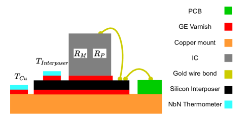
Figure 1 illustrates the IC configuration. The IC, a 2 mm x 2 mm x 0.8 mm chip, is affixed to a silicon interposer, mounted on a ultra-high-purity copper mount, which in turn is secured to the puck connected to the MXC. The device is interconnected via gold bond wires to gold traces on the interposer, and subsequently bonded to the printed circuit board (PCB). The IC contains a power resistor, , and a measurement resistor, . These components are fabricated using an industrial 65 nm bulk CMOS process. The entire assembly is cooled by an Oxford Instruments Triton 400 dilution refridgerator.
II.1 Measurement Principle
For a resistor with resistance at a temperature , the Johnson-Nyquist theorem Johnson (1928); Nyquist (1928) states that the power spectral density, , within a 1Hz bandwidth across the resistor is expressed as
| (1) |
Consequently, if the resistance is precisely known, the resistor can serve as a primary thermometer, with the temperature determined by
| (2) |
To determine , we calculate a cross-correlated spectrum to measure noise levels beneath the intrinsic noise of the amplifiers Chen and Van Der Ziel (1965); Wolff (1965). This demands the simultaneous acquisition of voltage as a function of time via two amplifier channels. The time traces of amplifiers and , denoted as and respectively, contain a shared signal, , alongside a noise component pertinent to the input noise of each amplifier, and . In this context, represents the thermal voltage originating from the resistor. The expressions for the amplifier signals are given by,
| (3) |
and
| (4) |
Each cross-correlation spectrum, , is derived by computing the dot product of the Fourier transform of one trace with the complex conjugate of the Fourier transform of the other,
| (5) |
The resultant spectrum are then averaged times to attenuate uncorrelated noise, yielding . With adequate averaging, this converges to the Fourier transform of the common signal,
| (6) |
Given the complex nature of this spectra, its magnitude is computed and subsequently scaled to account for the windowing effect during the Fourier transform. Finally, the average value over a frequency range encompassing points is calculated to produce our final value,
| (7) |
which is then converted to an Equivalent Noise Temperature (ENT) by Eq.2.
II.2 Detail of operation
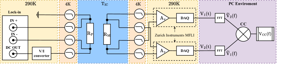
A diagram of the electrical set up of the experiment is given in Fig. 2. The time traces in our experiment were recorded using two Zurich Instruments MFLIs . Both amplifiers were synchronized and triggered via the Multi-Device Synchronization (MDS) package. To ensure the simultaneity of the traces, measurement timestamps from each amplifier were compared, ensuring that the traces commenced within a maximum of 20 . The amplifiers acquired data at 120 kHz, where denotes the clock frequency of 60 MHz, collecting samples. This configuration results in a measurement duration of 0.56 s per spectrum. Following the acquisition of both time traces, the cross-correlation spectrum was computed to attenuate non-correlated noise. This spectrum was subsequently averaged to further reduce residual noise. In our study, the number of averages was set to 3000, a value selected to limit the total measurement time to under 30 minutes. The requisite number of averages to sufficiently attenuate the measurement-specific noise floor is a function of both the noise, , (in ) of a single channel amplifier, and the noise floor targeted for resolution, . The number of averages to achieve a ratio of unity between the expected standard deviation of the measured value and the expected measured value is determined by
| (8) |
which follows Rubiola Rubiola and Giordano (2006) but conserves the contribution of the amplifier noise. Considering the number of averages and that at low frequencies the noise floor of a single channel is approximately , we can re-arrange Eq.8 to derive the minimum measurable noise floor,
| (9) |
This yields , corresponding to a minimum measurable temperature of approximately 100 mK (for ). Conversely, in the absence of cross-correlation, the minimum resolvable noise would be that of the amplifier at low frequencies, with an equivalent minimum temperature of 6.4 K. Five distinct frequency ranges were selected to compute an average spectral density. These ranges were determined by examining the base temperature spectra and identifying regions without frequency peaks generated from interference from other electrical sources.
II.3 Characterisation of measurement resistor
Preliminary noise measurements at a base temperature of indicated that the measurement resistor exhibited an anomalously elevated noise floor, as depicted in Fig. 3.
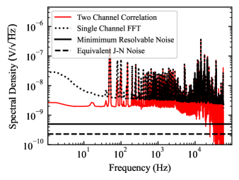
Although this noise level is lower than that of the amplifier, it possesses an ENT of 1.77 K. To ascertain that this observation was not an artifact of the experimental configuration, noise measurements across the resistor were also conducted in an alternative section of the setup (R = 9 k) and with a dead short of the measurement resistor, as illustrated in Fig. 4.
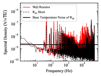
Both of these values are below the noise level of the measurement resistor at base temperature. This indicates that this excess noise is related to the measurement resistor and not the set up. We consider two options for the existence of this unexpectedly high noise level.
-
1.
does not thermalise with the MXC and instead saturates at the ENT of 1.77K.
-
2.
The noise is caused by a combination of the base temperature thermal contribution and a constant offset from the properties of the resistor itself.
Figure 5 illustrates the resistance of as a function of temperature.
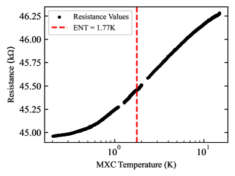
This was determined through four-terminal lock-in measurements with an AC current excitation of 500 pA at a frequency of 66 Hz, with 11 values recorded per temperature step and subsequently averaged. The absence of a resistance plateau at the noise equivalent temperature of 1.77 K implies that at these temperatures, the resistor remains thermalised to the MXC rendering scenario 1 unlikely. The precise origin of the noise was challenging to determine due to the unknown construction of the resistor. However, literature has shown that non-thermal noise is prevalent in silicon-based resistors at low temperatureDeen, Rumyantsev, and Orchard-Webb (1998). We consider this noise (denoted by ) to be temperature independent, thus treating it as an offset that can be subtracted from our correlated spectral values. To calculate this value, we take the a spectral measurement of the resistor at a well defined temperature, measure the resistance and then subtract the theoretically predicted Johnson-Nyquist value at this temperature. In practice this is performed at base temperature so to minimise the impact of error from the thermal noise contribution on the eventual noise offset value. The temperature at base was 15 mK based on the MXC thermometer reading. The theoretical base temperature contribution, , was calculated using this temperature and a resistance reading. The total spectral density at base after sufficient cross correlation averages, , is given by,
| (10) |
For the average spectra at every temperature step, x, , we remove , with the result ,
| (11) |
which is then converted into a ENT by averaging the values in a range of white noise frequencies.
III Noise Temperature vs MXC temperature
In order to verify noise thermometry we compared the noise temperature of the resistor against the MXC thermometers. We increased MXC from 100 mK to 8 K in twelve steps. At each temperature step the resistance was measured to ensure its value was well known. At each step spectra were recorded, processed and averaged according to Sec. II. The results of this experiment are shown in Fig. 6.
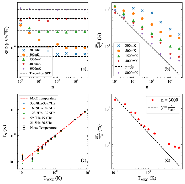
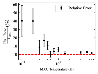
Further details on the agreement with the MXC temperature is provided in Fig. 7. Although the noise temperature generally aligns with the MXC temperature, it is only beyond 200 mK that the measured values begin to fall within the uncertainties of the MXC temperature. The uncertainty in the noise temperature also encompasses the uncertainty arising from the offset noise value. Therefore, employing a resistor without an offset will reduce the uncertainty across all temperature ranges. Additionally, due to the presence of noise offset, this method no longer qualifies as a form of primary thermometry. This is predicated on the assumption that the thermalises at the base temperature of 15 mK, an assumption that cannot be verified with certainty. Nonetheless, at temperatures exceeding 2 K, the impact of this assumption constitutes less than of the total value, rendering its effect almost negligible.
The principal limitation of this methodology is that the relative uncertainty is inversely proportional to the square root of the number of averages and inversely proportional to the temperature of the resistor. For instance, with 3000 averages, to achieve a relative uncertainty of less than 2, the maximum measurable temperature is approximately 1.5 K. Alternatively, limiting measurement time to 1 minute requires 100 averages. For a relative uncertainty of 2 this is limited to approximately 8 K or greater. Consequently, the primary constraint of this technique is the extended duration required for averaging to achieve lower temperatures and reduced relative uncertainties. The main solutions to this problem can be summarised as:
-
1.
Lower the input noise of the amplifiers.
-
2.
Decrease the time it takes to acquire one spectrum.
One such alternative set up would be the use of cryo-amps. The lower noise floor of the amplifiers would allow a lower resistance value to be used; this would, in turn, increase the cutoff frequency of the RC circuit created by the resistor and parasitic wire capacitance. A higher cut-off frequency would allow for a higher sampling rate and reduce the time per spectral acquisition. A good example of accurate high frequency noise thermometry would be Crossno et al Crossno et al. (2015).
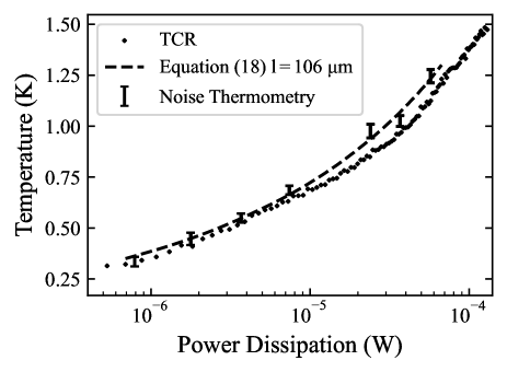
IV Noise temperature vs power dissipation
To substantiate noise thermometry, it was important to conduct in situ testing by applying power within the IC while simultaneously measuring the temperature. This validation step is crucial, as the proximity of a power-dissipating element to could potentially induce cross-talk, thereby compromising the accuracy of noise measurements. To validate the noise thermometry, we utilised an alternative in-IC methodology, specifically the TCR technique that employs . We used the temperature dependence characterised in Fig. 5 as a calibration reference against the MXC. Initially, we tested TCR thermometry in relation to power dissipation ranging from 600 nW to . This was to ensure the temperature was larger than 300 mK, at which temperatures the both the noise thermometer and TCR was considered to be accurate. At each increment, resistance measurements were taken and subsequently converted to temperature using the established calibration. Subsequently, to assess the noise thermometry, power was applied at seven levels, and at each level the spectra were processed and averaged in accordance with the methodology outlined in Sec. II. A baseline spectrum was recorded with the power resistor connected but without power dissipation to re-calibrate the offset spectral density. This was done to account for any potential cross-talk from the power resistor that might be present in all measurements.
The temperature inside the IC can be modelled in the idealised case that we consider the power source to be a point source at the centre of the top surface of the IC. We then consider the heat propagation to be radial from the heat source. We next have to consider, , the mean free path of phonons within the silicon. This value is not well defined but can be large (on the order of centimeters Swartz and Pohl (1989)) in pure silicon at low temperatures. If approaches the characteristic length scale of the phonon container (, in our case ) then the heat equation breaks down. This is because generating a temperature gradient requires multiple phonon scattering events throughout the length that is defined to have a gradient. In this case phonons are considered to behave ballistically, and the Boltzmann Transport Equation is more suited to describing the temperature profile Wang, Povolotskyi, and Vasileska (2024). However, in ICs there are many places to provide scattering events. In the case of substrates with high dopant concentrations, this could be the dopant centers. Another place for scattering events is the top layer of the IC, which contains many different types of materials, which at low temperature can cause phonon mismatch at the boundaries and therefore scattering. The Knudsen number () helps to determine the boundary between ballistic and diffusive energy carrier propagation Hahn and Özisik (2012) and is defined as
| (12) |
It gives the ratio between the characteristic distance an energy carrier travels () and the characteristic length scale of the system (). In our case
| (13) |
If , we can consider the system to act diffusively. If we use the diffusive model then the corresponding steady state heat equation is given by,
| (14) |
with the conductivity, . For silicon, this expression can be given by Savin et al. (2006); Swartz and Pohl (1989),
| (15) |
Equation 14 does not contain a source term as its assumed all of the heat is dissipated back into the MXC. To solve it, several boundary conditions are given; the first is,
| (16) |
where is the temperature of the silicon interposer at a given power. in our case is the distance from the power source to the silicon interposer, which is . Interestingly, the temperature of the interposer greatly exceeds the copper holder and the MXC temperature (see Appendix D) due to the large boundary resistance at the copper - varnish - interposer boundary. Next,
| (17) |
This boundary condition states that the heat flux is equal to the total power dissipated () divided by the area of hemisphere created by the radial movement of heat from the top surface. The solution to this equation is then,
| (18) |
where . The results of both TCR, noise thermometry and Eq. 18 fitted for are illustrated in Fig. 8. Both data sets exhibit reasonable degree of agreement, thereby substantiating the efficacy of noise thermometry across a range of power dissipation levels. However, variation in the different frequency bins at each measurement point suggests that this technique would be improved by increasing the number of point averaged, to average out this variation. These findings imply that this methodology could be suitable for application within ICs containing multiple power-consuming devices.
V Conclusions
We have established that noise thermometry exhibits broad agreement with other thermometry in the range 300 mK to 8 K. Furthermore, it shows substantial agreement the predicted temperature, when employed to determine the IC temperature corresponding to a specific power dissipation. This form of thermometry was made to be effective by the use of both cross-correlation and the subtraction of the offset noise calculated from base temperature measurements. This work suggests that with the addition of these techniques, voltage noise thermometry could be broadly applicable to ICs developed with industrial CMOS processes. However, the offset noise does precludes the noise thermometry in this paper from being a primary method of thermometry. Employing a resistor devoid of additional noise would reduce the measurement uncertainties and retain the technique as a primary thermometry method. Although this work demonstrates the increase in the uncertainty of measurements at lower temperatures and the large measurement time, we describe how the use of cold amplifiers could rectify both of these issues. Furthermore, as the direction of quantum computing moves towards temperatures closer to 1 K to access higher cooling powerCamenzind et al. (2022); Yang et al. (2020); Petit et al. (2018, 2020), this method will require less averaging to attenuate uncorrelated noise. This will mean faster measurements and lower uncertainties. In addition, the implementation of this technique is straightforward and requires only standard instruments that are typically available in academic or commercial laboratories. Given that the devices used are only resistors, this method significantly reduces the time and resources required for the design of ICs, facilitating the placement of thermometers at multiple locations within an IC. Finally, we suggest that this technique is an excellent candidate for performing in-IC temperature measurements to map the thermal profile of operational quantum-classical circuitry because of its dual primary and dissipationless nature.
VI Acknowledgments
This research is supported by the European Union’s Horizon 2020 research and innovation programme (European Microkelvin Platform 824109). The interposer device fabrication has been done at HNF - Helmholz Nano Facility, Research Center Juelich GmbH Albrecht, Moers, and Hermanns (2017).
VII Appendix
VII.1 Uncertainty in Temperature
The expectation relative error in the spectral measurement , the ratio of the expected standard deviation to the expected spectral value, is calculated from Rubiola and Giordano (2006). This is a function of the amplifier channels’ power spectral density, , the target noise level, , and the number of averages, n, we can look at how the relative error changes with temperature within our measurements. As,
| (19) |
and we know that then it follows that in the case that the relative error in the resistance is small, that,
| (20) |
In the low temperature case, where , this expression simplifies further,
| (21) |
We know that in our case in a 1Hz bandwidth and that is constant with temperature. As such, we can say,
| (22) |
VII.2 Uncertainty in Noise Temperature
Given the Johnson-Nyquist relationship between temperature and spectral density given in Eq. 2 the relative uncertainty in temperature, , is given by,
| (23) |
In this experiment, is given by the standard error of the resistance measurements taken at every temperature step, while is given by the average value. For the spectral density, is taken from the standard error of the values of the frequency values chosen to be averaged. However, because we have to remove an offset at each step, we need to take this into account. As
| (24) |
where is the measured spectral density and is the offset spectral density. We calculate by,
| (25) |
where is the base temperature measurement and is the Johnson-Nyquist value of the spectral density of the resistor at 15mK, assuming the resistor is well thermalised with the MXC. The only error in is the error of the resistance at base in this case,
| (26) |
Now we sum the errors of and in quadrature,
| (27) |
VII.3 Calibration of Niobium Nitride Thermometers
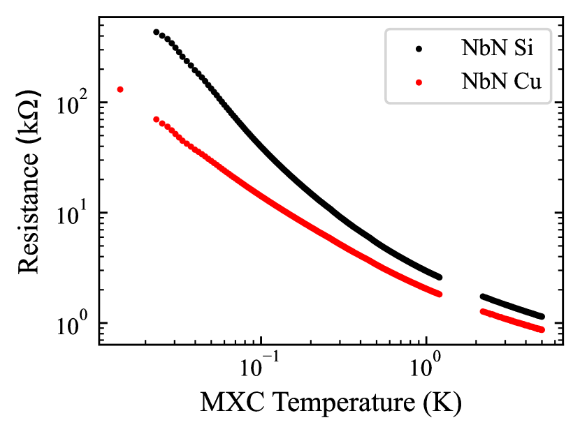
Niobium nitride thermometers were ideal candidates for monitoring both the copper and silicon interposer temperature due their excellent temperature sensitivity at milli-kevlin temperatures Bourgeois et al. (2006); Nguyen et al. (2019). Both the interposer and copper thermometers had their resistance read out standard 4 point AC lock-in technique. The input current was 0.2 nA at 81 Hz. During the calibration, ten points were taken per temperature step, with a settling time of 3 s per point and a 3 s sweep delay. The first step to ensure adequate thermalisation was that the MXC temperature had to return two consecutive temperature readings within a defined threshold of the target temperature before it allowed the values to be taken. The temperature steps were also made to be small to further reduce the risk of poor thermalisation. From 16 mK to 360 mK the temperature step was 2 mK, from 360 mK onwards it was 5 mK. Results of the calibration are shown in Fig 9.
VII.4 Silicon Interposer, Copper and Mixing Chamber Temperature as a Function of Power
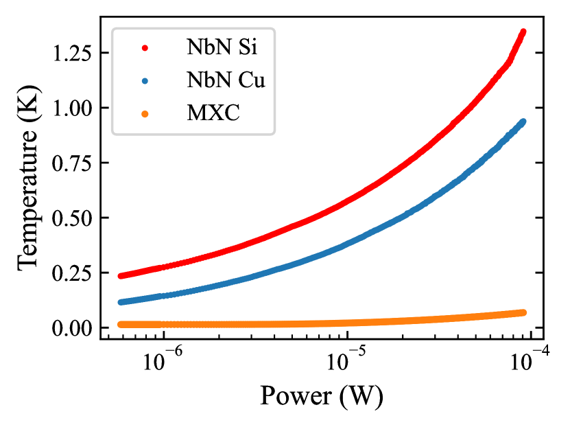
Figure 10) demonstrates the temperature of several different thermometers at different locations on the setup. All thermometers were read out under the same conditions as their calibration.
References
- Blagg, Castagnède, and Singh (2022) K. Blagg, A. Castagnède, and M. Singh, “On-chip heating effects in electronic measurements at cryogenic temperatures,” Cryogenics 126, 103536 (2022).
- Glassbrenner and Slack (1964) C. J. Glassbrenner and G. A. Slack, “Thermal conductivity of silicon and germanium from 3 k to the melting point,” Physical review 134, A1058 (1964).
- Chawner et al. (2019) J. Chawner, A. Jones, M. Noble, G. Pickett, V. Tsepelin, and D. Zmeev, “Lego® block structures as a sub-kelvin thermal insulator,” Scientific Reports 9, 1–4 (2019).
- Swartz and Pohl (1989) E. T. Swartz and R. O. Pohl, “Thermal boundary resistance,” Reviews of modern physics 61, 605 (1989).
- Brandl et al. (2016) M. Brandl, M. Van Mourik, L. Postler, A. Nolf, K. Lakhmanskiy, R. Paiva, S. Möller, N. Daniilidis, H. Häffner, V. Kaushal, et al., “Cryogenic setup for trapped ion quantum computing,” Review of Scientific Instruments 87 (2016).
- Córcoles et al. (2011) A. D. Córcoles, J. M. Chow, J. M. Gambetta, C. Rigetti, J. R. Rozen, G. A. Keefe, M. Beth Rothwell, M. B. Ketchen, and M. Steffen, “Protecting superconducting qubits from radiation,” Applied Physics Letters 99 (2011).
- Veldhorst et al. (2017) M. Veldhorst, H. Eenink, C.-H. Yang, and A. S. Dzurak, “Silicon cmos architecture for a spin-based quantum computer,” Nature communications 8, 1766 (2017).
- Gonzalez-Zalba et al. (2021) M. Gonzalez-Zalba, S. De Franceschi, E. Charbon, T. Meunier, M. Vinet, and A. Dzurak, “Scaling silicon-based quantum computing using cmos technology,” Nature Electronics 4, 872–884 (2021).
- Pauka et al. (2021) S. Pauka, K. Das, R. Kalra, A. Moini, Y. Yang, M. Trainer, A. Bousquet, C. Cantaloube, N. Dick, G. Gardner, et al., “A cryogenic cmos chip for generating control signals for multiple qubits,” Nature Electronics 4, 64–70 (2021).
- Courts (2014) S. S. Courts, “A standardized cernox™ cryogenic temperature sensor for aerospace applications,” Cryogenics 64, 248–254 (2014).
- Courts and Krause (2008) S. Courts and J. Krause, “A commercial ruthenium oxide thermometer for use to 20 millikelvin,” in AIP Conference Proceedings, Vol. 985 (American Institute of Physics, 2008) pp. 947–954.
- Dechaumphai and Chen (2014) E. Dechaumphai and R. Chen, “Sub-picowatt resolution calorimetry with niobium nitride thin-film thermometer,” Review of Scientific Instruments 85 (2014).
- Huizinga et al. (2022) T. Huizinga, M. Babaie, A. Vladimirescu, F. Sebastiano, et al., “Integrated cryo-cmos temperature sensors for quantum control ics,” in 2022 IEEE 15th Workshop on Low Temperature Electronics (WOLTE) (IEEE, 2022) pp. 1–4.
- Noah et al. (2024) G. M. Noah, T. H. Swift, M. De Kruijf, A. Gomez-Saiz, J. J. Morton, and M. F. Gonzalez-Zalba, “Cmos on-chip thermometry at deep cryogenic temperatures,” Applied Physics Reviews 11 (2024).
- Triantopoulos et al. (2019) K. Triantopoulos, M. Cassé, S. Barraud, S. Haendler, E. Vincent, M. Vinet, F. Gaillard, and G. Ghibaudo, “Self-heating effect in fdsoi transistors down to cryogenic operation at 4.2 k,” IEEE Transactions on Electron Devices 66, 3498–3505 (2019).
- Artanov et al. (2022) A. A. Artanov, E. A. Gutiérrez-D, A. R. Cabrera-Galicia, A. Kruth, C. Degenhardt, D. Durini, J. Méndez-V, and S. Van Waasen, “Self-heating effect in a 65 nm mosfet at cryogenic temperatures,” IEEE Transactions on Electron Devices 69, 900–904 (2022).
- Chawner et al. (2021) J. Chawner, S. Barraud, M. Gonzalez-Zalba, S. Holt, E. Laird, Y. A. Pashkin, and J. Prance, “Nongalvanic calibration and operation of a quantum dot thermometer,” Physical Review Applied 15, 034044 (2021).
- de Kruijf et al. (2024) M. de Kruijf, G. M. Noah, A. Gomez-Saiz, J. J. Morton, and M. F. Gonzalez-Zalba, “Measurement of cryoelectronics heating using a local quantum dot thermometer in silicon,” Chip , 100097 (2024).
- Singh et al. (2024) S. K. Singh, D. Sharma, P. Srinivasan, and A. Dixit, “Quantum-dot-based thermometry using 12-nm finfet and machine learning models,” IEEE Transactions on Electron Devices (2024).
- Choi et al. (2021) A. Y. Choi, I. Esho, B. Gabritchidze, J. Kooi, and A. J. Minnich, “Characterization of self-heating in cryogenic high electron mobility transistors using schottky thermometry,” Journal of Applied Physics 130 (2021).
- Bebitov et al. (2023) R. Bebitov, O. Abdulkhaev, D. Yodgorova, D. Istamov, G. Khamdamov, S. M. Kuliyev, A. Khakimov, and A. Rakhmatov, “Dependence of the accuracy of the silicon diode temperature sensors for cryogenic thermometry on the spread of their parameters,” Low Temperature Physics 49, 256–260 (2023).
- Qu et al. (2019) J. Qu, S. Benz, H. Rogalla, W. Tew, D. White, and K. Zhou, “Johnson noise thermometry,” Measurement Science and Technology 30, 112001 (2019).
- Casey et al. (2014) A. Casey, F. Arnold, L. V. Levitin, C. P. Lusher, J. Nyéki, J. Saunders, A. Shibahara, H. Van Der Vliet, B. Yager, D. Drung, et al., “Current sensing noise thermometry: a fast practical solution to low temperature measurement,” Journal of Low Temperature Physics 175, 764–775 (2014).
- Ivashchenko, Korobchenko, and Bondarenko (1975) Y. S. Ivashchenko, Y. G. Korobchenko, and T. Bondarenko, “Electron temperature of a hydrocarbon flame,” Combustion, Explosion and Shock Waves 11, 703–707 (1975).
- Brixy and Kakuta (1996) H. Brixy and T. Kakuta, “Noise thermometer (jaeri review 96-003),” Tokaimura: Japan Atomic Energy Research Institute (1996).
- Wilamowski and Irwin (2018) B. M. Wilamowski and J. D. Irwin, Fundamentals of industrial electronics (CRC Press, 2018) Chap. 11.
- Johnson (1928) J. B. Johnson, “Thermal agitation of electricity in conductors,” Physical review 32, 97 (1928).
- Nyquist (1928) H. Nyquist, “Thermal agitation of electric charge in conductors,” Physical review 32, 110 (1928).
- Chen and Van Der Ziel (1965) T.-M. Chen and A. Van Der Ziel, “Hanbury brown—twiss type circuit for measuring small noise signals,” Proceedings of the IEEE 53, 395–395 (1965).
- Wolff (1965) S. Wolff, “On the brown-twiss circuit,” Proceedings of the IEEE 53, 1140–1141 (1965).
- Rubiola and Giordano (2006) E. Rubiola and V. Giordano, “On the 1/f frequency noise in ultra-stable quartz oscillators,” in 2006 IEEE International Frequency Control Symposium and Exposition (IEEE, 2006) pp. 759–766.
- Deen, Rumyantsev, and Orchard-Webb (1998) M. Deen, S. Rumyantsev, and J. Orchard-Webb, “Low frequency noise in heavily doped polysilicon thin film resistors,” Journal of Vacuum Science & Technology B: Microelectronics and Nanometer Structures Processing, Measurement, and Phenomena 16, 1881–1884 (1998).
- Crossno et al. (2015) J. Crossno, X. Liu, T. A. Ohki, P. Kim, and K. C. Fong, “Development of high frequency and wide bandwidth johnson noise thermometry,” Applied Physics Letters 106 (2015).
- Wang, Povolotskyi, and Vasileska (2024) Z. Wang, M. Povolotskyi, and D. Vasileska, “Modeling thermal effects for 28-nm node fully depleted soi devices under cryogenic temperatures,” IEEE Transactions on Electron Devices (2024).
- Hahn and Özisik (2012) D. W. Hahn and M. N. Özisik, Heat conduction (John Wiley & Sons, 2012).
- Savin et al. (2006) A. Savin, J. P. Pekola, D. Averin, and V. Semenov, “Thermal budget of superconducting digital circuits at subkelvin temperatures,” Journal of applied physics 99 (2006).
- Camenzind et al. (2022) L. C. Camenzind, S. Geyer, A. Fuhrer, R. J. Warburton, D. M. Zumbühl, and A. V. Kuhlmann, “A hole spin qubit in a fin field-effect transistor above 4 kelvin,” Nature Electronics 5, 178–183 (2022).
- Yang et al. (2020) C. H. Yang, R. Leon, J. Hwang, A. Saraiva, T. Tanttu, W. Huang, J. Camirand Lemyre, K. W. Chan, K. Tan, F. E. Hudson, et al., “Operation of a silicon quantum processor unit cell above one kelvin,” Nature 580, 350–354 (2020).
- Petit et al. (2018) L. Petit, J. Boter, H. Eenink, G. Droulers, M. Tagliaferri, R. Li, D. Franke, K. Singh, J. Clarke, R. Schouten, et al., “Spin lifetime and charge noise in hot silicon quantum dot qubits,” Physical review letters 121, 076801 (2018).
- Petit et al. (2020) L. Petit, H. Eenink, M. Russ, W. Lawrie, N. Hendrickx, S. Philips, J. Clarke, L. Vandersypen, and M. Veldhorst, “Universal quantum logic in hot silicon qubits,” Nature 580, 355–359 (2020).
- Albrecht, Moers, and Hermanns (2017) W. Albrecht, J. Moers, and B. Hermanns, “Hnf-helmholtz nano facility,” Journal of large-scale research facilities JLSRF 3, A112–A112 (2017).
- Rothfuss et al. (2016) D. Rothfuss, A. Reiser, A. Fleischmann, and C. Enss, “Noise thermometry at ultra-low temperatures,” Philosophical Transactions of the Royal Society A: Mathematical, Physical and Engineering Sciences 374, 20150051 (2016).
- Oka et al. (2023) H. Oka, T. Inaba, S. Shitakata, K. Kato, S. Iizuka, H. Asai, H. Fuketa, and T. Mori, “Origin of low-frequency noise in si n-mosfet at cryogenic temperatures: The effect of interface quality,” IEEE Access (2023).
- Nguyen et al. (2019) T. Nguyen, A. Tavakoli, S. Triqueneaux, R. Swami, A. Ruhtinas, J. Gradel, P. Garcia-Campos, K. Hasselbach, A. Frydman, B. Piot, et al., “Niobium nitride thin films for very low temperature resistive thermometry,” Journal of Low Temperature Physics 197, 348–356 (2019).
- Bourgeois et al. (2006) O. Bourgeois, E. André, C. Macovei, and J. Chaussy, “Liquid nitrogen to room-temperature thermometry using niobium nitride thin films,” Review of scientific instruments 77 (2006).
- Harrison (1968) J. Harrison, “Cryostat for the measurement of thermal conductivity and specific heat between 0.05 and 2 k,” Review of Scientific Instruments 39, 145–152 (1968).
- White (1953) G. White, “The thermal conductivity of gold at low temperatures,” Proceedings of the Physical Society. Section A 66, 559 (1953).