Interaction of dopants with the I3-type basal stacking fault in hexagonal-diamond Si
Abstract
Recently synthesized hexagonal-diamond silicon, germanium, and silicon-germanium nanowires exhibit remarkable optical and electronic properties when compared to cubic-diamond polytypes. Because of the metastability of the hexagonal-diamond phase, I3-type basal stacking faults are frequently observed in these materials. In the present study, we employ density functional theory calculations to investigate the interaction of extrinsic dopants (group III, IV, and V elements) with the I3-type basal stacking fault in hexagonal-diamond silicon. Contrary to the behavior observed in cubic-diamond silicon with intrinsic stacking faults, we demonstrate that neutral and negatively charged -type impurities exhibit a marked tendency to occupy lattice sites far from the I3-type basal stacking fault. The interaction of acceptors with the planar defect reduces their energetic stability. However, this effect is much less pronounced for neutral or positively charged -type dopants and isovalent impurities. The thermodynamic energy barrier to segregation for these dopants is small and may even become negative, indicating a tendency to segregate into the fault. Through a detailed analysis of structural modifications, ionization effects, and impurity-level charge density distribution, we show that the origin of this behavior can be attributed to variations in the impurity’s steric effects and its wave function character. Finally, all these results are validated by considering the extreme case of an abrupt hexagonal/cubic silicon interface, where acceptor segregation from the cubic to the hexagonal region is demonstrated, confirming the behavior observed for -type dopants near to the I3-type defect.
Keywords: hexagonal-diamond, stacking faults, DFT, Si, doping, segregation.
1 Introduction
Silicon (Si), Germanium (Ge), and SiGe alloys are the building blocks of the microelectronics and nanoelectronics industry. However, the cubic-diamond (cub) structure in which they typically crystallize presents an indirect bandgap, limiting their use in optical devices. To overcome this limitation, several groups have recently succeeded in synthesizing group IV hexagonal-diamond (hex) polytypes in the form of nanowires (NWs) [1, 2, 3, 4, 5, 6]. Indeed, while hex-Si remains an indirect bandgap material, both its indirect and direct bandgaps are reduced compared to cub-Si, making it promising for photovoltaic applications [7, 8]. Furthermore, Ge and SiGe alloys with a higher concentration of Ge exhibit a direct bandgap [6, 9, 10, 8, 11, 12, 13] which is associated with a luminescence in the infrared spectral range.
Recent structural characterization studies of hex-Si, hex-Ge, and hex-SiGe have reported the presence of planar defects [3, 6, 14, 15, 16, 17], with the I3-type basal stacking fault (I3-BSF) being the most common. This intrinsic defect arises from the substitution of a B-plane in the typical ABABABAB stacking sequence of the hexagonal phase with a C plane. Viewed along the crystallographic direction, this defect manifests itself as a sequence of two twinned cubic cells with a hexagonal one in between, i.e., I3-BSF introduces two symmetric rows of atoms with cubic-like bonding within the hexagonal structure [14]. Note that I3-BSF usually does not extend through the nanowire, taking only a part of 0001 planes. The defective planes terminate in directions with 30∘ partial dislocations, usually giving rise to a triangular-shaped defect [15, 14, 16]. Neither the defective atomic layers nor the dislocations introduce any strain in the system. Indeed, the dislocations in the two adjacent defective planes have opposite Burgers vectors, canceling the relative deformation field. Several studies have demonstrated that they may arise from the growth kinetics under specific conditions [15, 16], and they do not introduce any additional states within the bandgap of hex-Si and hex-Ge [14], thus not affecting the optical properties of the materials.
Nevertheless, planar defects can strongly influence dopant distribution and significantly impact the structural and electronic properties, as demonstrated in the case of cub-Si [18, 19, 20, 21, 22, 23]. Therefore, it is crucial to understand the impurity behavior close to extended defects, as dopant accumulation may affect their electrical activation and degrade device performance. Although extrinsic doping in hex-Si, hex-Ge, and hex-SiGe has been experimentally achieved [6, 17], characterizing the interaction of dopants with extended defects remains challenging due to the difficulty of providing a precise chemical characterization at the relevant defect scale. From a theoretical perspective, while doping and point defects in hex-Si and hex-Ge have already been studied by ab initio methods [24, 25, 26, 9, 27], the effects of the I3-BSFs on the doping properties remain unaddressed.
In this work, we employ density functional theory (DFT) simulations to investigate the interaction of -type and -type dopants with the I3-BSF in hex-Si. Note that we consider I3-BSF as infinitely extended (dislocations bounding the I3-BSF are not modeled), looking at the local interaction of dopants with the defective layers. Through a careful structural and energetic analysis, we demonstrate that neutral and negatively charged acceptors prefer to occupy lattice sites far from the I3-BSF. Nevertheless, this behavior is less marked for ionized acceptors. Neutral and positively charged donors and isovalent impurities do not show the same trend because their segregation energy is minimal and can be negative when the dopant is close to the fault. A detailed analysis of structural modifications, ionization effects, and charge density distributions proves that the origin of this different behavior can be ascribed to a variation in the steric effect and the dopant wave function localization.
Finally, we demonstrate that the segregation of -type dopants towards a hexagonal-like environment is also present in the extreme case of an abrupt hex/cub Si interface, thus confirming the results obtained for -type dopants in the proximity of the I3-BSF.
2 Computational Details
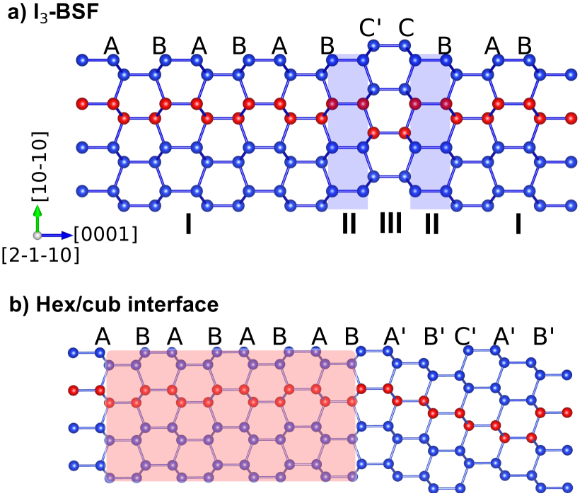
Spin-polarized ab initio DFT simulations were performed using the SIESTA code [28]. The generalized gradient approximation (GGA) with the Perdew, Burke, and Ernzerhof (PBE) functional [29] was used. Since experimentally grown hexagonal nanowires typically have diameters greater than 10 nm, quantum confinement effects on the bandgap can be neglected [30, 31, 32, 33, 1, 34]. Therefore, we used bulk supercells as an accurate and reliable approximation for these larger-diameter nanowires. A double- polarized basis set was used for the valence electrons of Si, while a double- basis set plus two polarization orbitals was employed for the dopant atoms. Inner core electrons were replaced by norm-conserving pseudopotentials of the Troullier-Martins type [35]. The hex-Si crystal cell was optimized using an 888 k-point grid generated with the Monkhorst-Pack sampling [36]. The optimized lattice parameters, Å and Å, are in good agreement with values reported in previous works employing the same type of exchange-correlation functional [8, 9]. Extrinsic doping was analyzed in the hex-Si crystal, both pristine and with an I3-type BSF. A 446 supercell (see Figure 1a) was used. These cell dimensions are sufficiently large to minimize the spurious electrostatic interaction between the periodic images of dopants and BSFs. The structure is composed of ten layers of hex-Si along the direction (c-axis of the hexagonal structure), interspersed with two cubic-diamond stoichiometry planar defects (see the light blue rectangles in Figure 1a) and a hexagonal region between them. The supercell contains 384 atoms and, when doped, leads to a doping concentration of (one or two orders of magnitude larger than the one measured in the experimental samples [6, 17]).
We considered common substitutional dopant atoms in Si: acceptors (B, Al, Ga, In), donors (N, P, As, Sb), and isovalent impurities (C, Ge). All the atomic positions in doped and undoped systems were optimized using a conjugate gradient algorithm that calculates DFT forces through the Hellmann-Feynman theorem. Structural convergence was achieved when the forces were less than 10-2 eV/Å and the stress was lower than 10-1 GPa. A 221 Monkhorst-Pack k-point grid and a mesh cutoff of 500 Ry were carefully chosen to ensure the correct convergence of total energies and forces. For charged impurity calculations, an electron was added or subtracted with the inclusion of a compensating jellium background to maintain charge neutrality and avoid divergence of the electrostatic energy. The structures containing the charged impurities were optimized, starting from the previously relaxed neutral-doped configurations, using the same convergence parameters setup.
The results obtained for hex-Si with the I3-BSF were then compared with the case of an abrupt hex/cub-Si interface (Figure 1b), built along the hexagonal crystal direction. Such an interface comprises eight hexagonal and six cubic layers and has 448 atoms. Even in this case, the doping concentration is about . By calculating DFT ground-state total energy and the corresponding charge density distribution, we investigated the effect of the I3-BSF on the dopant behavior and the electronic properties of the system. To this end, we relaxed several defect configurations with a substitution atom positioned at different layers along the c-axis (highlighted in red in Figure 1), and for each configuration, we calculated the dopant segregation energy (DSE). As in previous works [23, 20], the DSE is defined here as the difference between the ground state energy of the doped system with the fault, , and reference energy where the interaction with the stacking fault is minimized. The supercell size was hence converged to ensure that the total energy of the system with the dopant positioned at the farthest distance from the I3-BSF (denoted as ) coincides with the sum of the doped pristine supercell and the stacking fault energy (the difference between the two values is less than 0.01 eV). Therefore, the DSE is expressed as
| (1) |
where is the total energy of the defective system with the dopant at position , and is the total energy when the dopant is at the farthest atomic plane from the defect. Negative values of DSE correspond to an attraction between the I3-BSF and the dopant, while positive values indicate that segregation is thermodynamically unfavored. The DSE provides a quantitative evaluation of the dopant-stacking fault interaction and is determined by two primary contributions: the structural relaxation energy of the lattice induced by the dopant and the electrostatic interaction between the dopant and the I3-BSF.
3 Results and discussion
We start our analysis by calculating the stacking fault energy () defined as the energy difference normalized by the surface area between the total ground-state energy of the supercell containing the stacking fault, , and that of the pristine hexagonal phase, . This can be expressed as:
| (2) |
We found , which is compatible with the metastability of the hexagonal phase, whose total DFT ground-state energy is nearly 10-20 meV higher than the Si cubic phase [37]. These findings also agree with the negative formation energies reported in the literature [14] suggesting that defects like I3-type BSFs are energetically stable in such crystals. The thermodynamic preference may be related to the distinct symmetries of hexagonal and cubic polytypes, associated with different total energies. In particular, the Si hexagonal pristine structure exhibits a C3v symmetry, characterized by three equal bonds in the basal plane and a longer one perpendicular to it, which leads to a reduced bond strength along this direction. On the other hand, cubic crystal structures, such as those introduced by the I3-BSF, display a perfect tetrahedral symmetry (), where four equivalent bonds match the hybridization of the four valence electrons in Si, thus inducing higher chemical stability and lower total energy if compared to hex-Si. Moreover, it is worth noting that previous works [24, 25, 27] demonstrated that the stability of a dopant in one of the two bulk fault-free phases also depends on a complex interplay between the local structural environment around the dopant (induced by the symmetry of the host crystal), its atomic radius as well as and its valence). In particular, in hex-Si, acceptors have lower formation energy, present a symmetry, and have charge transition levels shallower with respect to the cub-Si case. On the other hand, donors are more stable in the cubic phase where they adopt a symmetry and have transition levels energies shallower with respect to hex-Si [24, 25, 27].
The hexagonal structure containing the I3-BSF, shown in Figure 1a, can be conceptually divided into three regions. Region I corresponds to the hexagonal Si bulk-like crystal structure (ABABAB in Figure 1a). Region II includes the two cubic arrangements induced by the I3-BSF, which breaks the hexagonal stacking sequence (BC’ and BC in Figure 1a). Region III lies between these two cubic sections and presents a hex-type structure (C’C in Figure 1a).
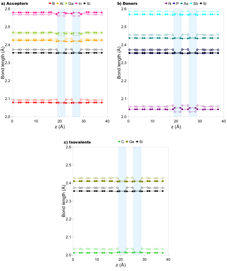
We begin the structural analysis by examining the local symmetry around the dopant. The dopant first neighbors bond lengths in the basal plane were averaged and compared to those along the perpendicular axis. As previously discussed, both donors and acceptors preserve the symmetry in bulk cub-Si where all the dopant’s first neighbors’ distances are equivalent [38, 39, 40]. This situation changes in the case of hex-Si, where both acceptors and donors are characterized by a marked C3v symmetry [27]. Figure 2 shows the averaged bond distances of the dopant first neighbors in the basal plane (continuous lines with solid circles) and along the c-axis direction (dashed lines with empty diamonds) for i) acceptors, ii) donors, and iii) isovalent impurities in hex-Si, located at the positions highlighted in red in Figure 1a. When the two lines overlap, the local symmetry is while it becomes of C3v-type when they differ. Each subplot includes reference data from the undoped structure for comparison (black lines). For the undoped hex-Si system containing the I3-BSF, there is a clear transformation in the local symmetry, which transitions from C3v in Region I to in Region II and back to C3v in Region III. When a dopant is introduced, the bond distances expand or contract depending on its covalent radius. As shown in Figure 2a and demonstrated in other works [25, 38, 39, 40], shorter interatomic distances in bulk Si correlate with smaller dopant covalent radii. However, from Figure 2a, it is clear that the distance of the dopant from the I3-BSF influences its bond lengths and local symmetry.
In particular, in Figure 2a, a transition from C3v to in Region II (BC’ and CB layers) is clear for B and Al. The same symmetry transformation holds for larger radius acceptors at the interfaces between Region I and II and between Region II and III. These acceptors also show a C3v symmetry in the cubic Region II. Interestingly, the bond lengths along the direction are shorter for these cases than those in the basal plane. For donors (Figure 2b) and for isovalent dopants (Figure 2c), the symmetry around impurities also passes from C3v to in Region II. A noteworthy exception to this behavior is represented by the case of N (Figure 2b). Indeed, although most of the dopants considered in cub-Si maintain a tetrahedral symmetry, both theoretical and experimental works demonstrated that N presents a local trigonal symmetry due to its low solubility in cub-Si [24, 25, 41, 42].
Looking at Figure 2a, it is clear that the effect of the I3-BSF on the dopant local symmetry in hex-Si is negligible when the dopant is far from the planar defect. The impact is merely localized to the lattice sites in proximity of the planar defect, with bond distances and symmetries in the various crystallographic regions matching those observed in doped bulk materials [24, 25, 27]. When the impurity lies in the bulk-like region far from the stacking fault, for both -type and -type dopants, the local symmetry is C3v as demonstrated in the case of doped bulk hex-Si [24, 25, 27]. If the dopant occupies positions close to the I3-BSF, there is a transition from the C3v to the , driven by the presence of the two symmetric cubic layers in the I3-BSF.
3.1 Segregation energy
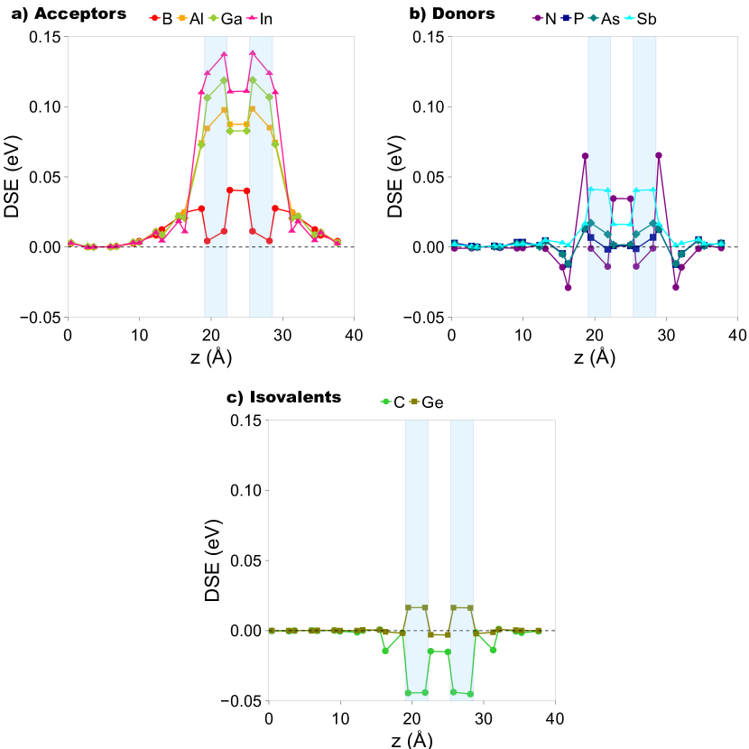
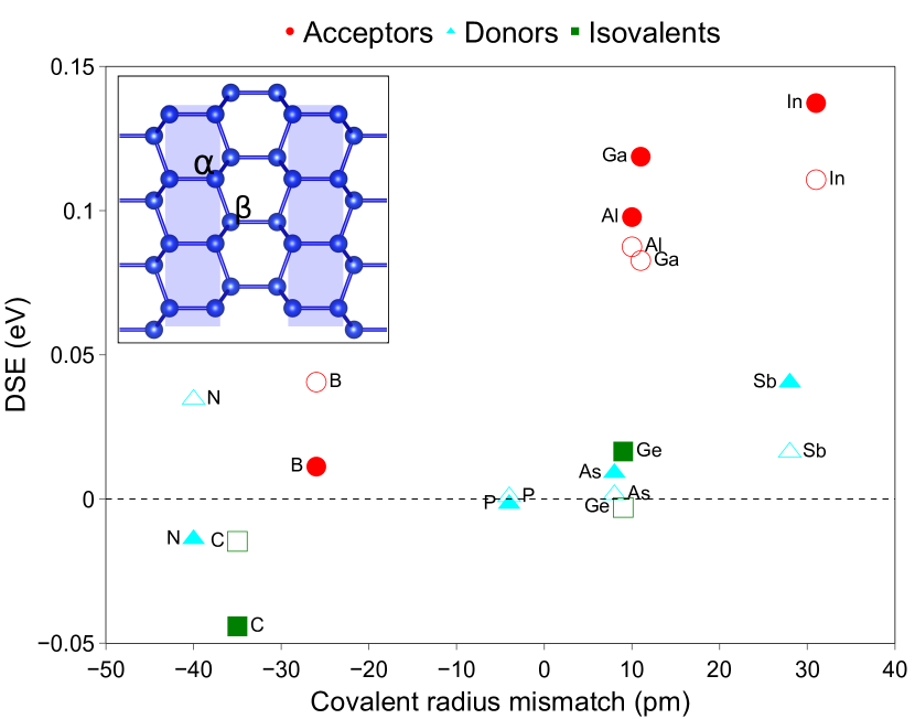
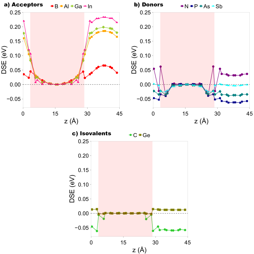
Figure 3 shows the dopant segregation energy (DSE) in hex-Si, calculated using Eq. 1, for acceptors, donors, and isovalent dopants along the red path of Figure 1a. As shown in other works [43, 44], a negative value of this quantity suggests that the attraction between the dopant and the planar defect is favored. In contrast, a positive value avoids the segregation toward the stacking fault. For all the neutral acceptors — with the noticeable exception of B —, the DSE is always positive close to the I3-BSF, reaching maximum values of 80-140 meV in Region II and 70-110 meV in Region III. The significant DSE differences between Regions I (hexagonal bulk-like environment) and II/III (basal stacking fault) suggest a thermodynamic driving force for acceptors to occupy lattice sites in the hexagonal pristine region and a dopant depletion near the I3-BSF. These findings may be put in relation to the work of Yamamoto et al. [22], in which it was theoretically predicted that dopants in cub-Si tend to segregate towards single intrinsic stacking faults. The negative segregation energies they calculated (100 meV for Al, 90 meV for Ga, and 130 meV for In) are of the same magnitude as the thermodynamic energetic barriers obtained here but present an opposite sign. Our results show that B does not follow this trend, presenting a very low DSE of approximately 40 meV in Region III and 30 meV at the boundary between Regions I and II. This particular result was further confirmed by plane waves DFT-GGA simulations we performed using the Quantum Espresso code [45]. Though unexpected, this behavior for B was also observed in the case of cub-Si containing intrinsic stacking faults [22], and it is related to the significant radius mismatch between B and Si atoms.
As for neutral donors (Figure 3b), DSEs are less pronounced than for acceptors, but neither here any relevant segregation into the stacking fault can be predicted. The maximum DSEs in Region II are around 40 meV for Sb and 20 meV for As and P. These DSEs are smaller than the ones reported in the case of cub-Si containing an intrinsic stacking fault [18, 22]. In the case of N, our results show a maximum energy peak of 70 meV between Region I and II and around 35 meV in Region III. This difference in the trend of DSE can be associated with the N particular symmetry in Si and its minimal atomic radius. Finally, the DSEs of C and Ge in Region II are lower than 20 meV, being even negative for C, suggesting a possible segregation behavior for this impurity.
As clearly explained in Ref. [46], the DSE may be separated into two main contributions: the elastic energy that is due to the packing local rearrangement of the dopant and the long-range electrostatic interaction of the dopant with the stacking fault. Though it is complicated to extract and separate the two contributions from the calculated DFT total energy, we tried to evaluate them by looking at the dependence of the DSE on the dopant charge state and the covalent radius mismatch between the dopant and the Si host atom.
Ionization effects.
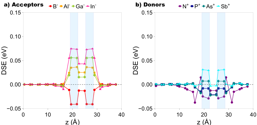
To examine the role of the dopant charge state, we evaluate the DSE in the case of negatively charged acceptors and positively charged donors here reported in Figure 4a and Figure 4b. Extended supercells have been used (see Figure 1a) to minimize the spurious long-range interactions between periodic images [47]. The residual electrostatic contribution for a given dopant will be independent of its position. Therefore, any other spurious coulomb term mostly cancels out since the DSE is calculated as a difference in energy between different dopant configurations (see Eq. 1).
Looking at Figure 4, one can observe that when an electron is added or removed, the DSE in the proximity of the I3-BSF is reduced. In particular, the DSE reduction for Al-, Ga-, and In- is 43-62 % in Region II, and 61-80 % in Region III. Despite this decrease, DSEs for In-, Ga- are still relevant, with values of 73 meV and 55 meV in Region II. Al- presents a less significant DSE of 34 meV in Region II. On the other hand, B- has a negative segregation energy of -40 meV close to the fault, indicating higher stability in the cubic-like region. Regarding positively charged donors, the DSE is strongly reduced to negligible or negative values in Region II. These results allow us to depict a first general trend: neutral and charged -type dopants prefer to occupy lattice sites far from the stacking fault plane, while neutral and charged -type impurities do not have any clear preference. The ionization reduces the thermodynamic energy barrier to segregation with respect to the neutral case. This means charged dopant ions reveal a reduced interaction with the I3-BSF. However, as the DSE has an electrostatic and elastic component, the ionization effect alone cannot explain the difference in the DSE trend among -type and -type dopants.
Steric effects.
To give an estimation of the elastic energy involved in the dopant-stacking fault interaction, we report in Figure 5 the magnitude of the DSE as a function of the covalent radius mismatch with the Si atom for all the considered neutral dopants. As can be seen, the DSE increases almost linearly with the radius mismatch. In particular, dopants with larger radius compared to Si (In, Ga, Al) have positive and larger values of the DSE. When the radius mismatch gets smaller (as in the case of Ge, P, and As), the DSE is very close to zero. Finally, very small radius dopants (N, B, and C) induce a zero or negative DSE. Further confirmation of these findings is given by comparing the DSE for all the considered cases with and without geometrical optimization, as reported in Figure S1 of the Supplemental Materials (SM). From the figure, it is clear that when the lattice mismatch is large, the difference between the relaxed and unrelaxed DSE is relevant (B, Ga, In, Al), while it is negligible when the radius mismatch is tiny (P, As, Ge). More in general, these results complement the physical picture drawn with the ionized impurity results: the I3-BSF defect represents a thermodynamic barrier in energy for acceptors because of both an electrostatic Coulomb repulsion and the large positive radius mismatch with Si. In contrast, donors — except for N — do not see the I3-BSF as a barrier, in particular when they are ionized. In this case, the elastic energy variation due to the covalent radius mismatch is not relevant to the interaction with the fault. As for isovalent impurities, the DSE is negligible for Ge, as expected, while it is negative for C due to the significant negative radius mismatch. This means that the I3-BSF could represent an energy sink for C atoms. Finally, it is worth noting that B represents a particular exception to the discussed trends. Indeed, ionization effects and radius mismatch are much more pronounced for this dopant than other acceptors. As in the case of C, B- atoms could segregate into the staking fault with negative DSE values.
Symmetry effects.
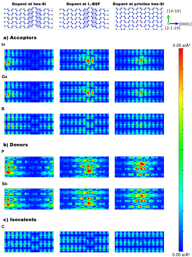
As previously pointed out, for both -type and -type dopants, the interaction with the I3-BSF is associated with a change in the local symmetry. In particular, the symmetry observed in pristine hex-Si and lattice sites far from the fault becomes one due to the presence of the two cubic layers (see Figure 1 and Figure 2). To understand if this change could affect the symmetry and localization of the dopant wave function and the DSE trends, we carefully analyzed the charge density distribution for all the considered neutral dopants, moving from the hexagonal bulk-like environment toward the stacking faults planes. We first analyzed the spatial distribution of the charge density in the I3-BSF system without any impurity (see Figure S2 of the SM). As reported in previous theoretical works [14], the presence of the I3-BSF does not perturb too much the valence band maximum (VBM) and conduction band minimum (CBM) if compared with the pristine hex-Si. However, the VBM charge density is depleted for the defective structure at the stacking fault region. This means, as already observed in the case of wurtzite GaN with cubic stacking faults [48], that the I3-BSF has a long-range influence of the VBM wave function (see Figure S2 of the SM). The behavior is different when an impurity is added to the system. In Figure 6, the charge density distribution associated with the defect level at the point is plotted for acceptors, donors, and isovalent impurities in three different cases: i) when the dopant is far from the stacking fault (left column), ii) when the dopant occupies a lattice site close to the stacking fault plane (central column), and iii) when the impurity atom is added to the pristine hex-Si bulk structure (right column). As it can be evinced from Figure 6a, in the case of acceptors (In, Ga, B), the impurity level wave function has a marked nature in the pristine hex-Si and the lattice sites away from the fault plane. Indeed, in both cases (left and right columns of Figure 6a), the electron density at the two bonds of the dopant atom lying in the plane of the cut is different, with the bond normal to the stacking fault having a lower density than the other one. This is due to the trivalent valence of acceptors whose ground state wave function fits the symmetry of the host hex-Si. In contrast, when the acceptor is near the stacking fault, the dopant wave function is more spatially localized, assuming a clear character due to the previously described structural changes. Indeed, in this case (central column of Figure 6a), the electron density at the two bonds of the dopant atom lying in the plane of the cut is very similar. This further contributes to the explanation of the segregation trends: the DSEs close to the I3-BSF plane are significant and positive because of the strong steric effect that forces the impurity level wave function to lose its ground state acceptor character and to assume a symmetry. Moreover, the charge density of the impurity level in the fault plane is higher than in the hexagonal bulk-like region, which further explains the high energetic instability.
The situation is entirely different in the case of donors (P, Sb) (see Figure 6b). Here, the presence of the stacking fault does not affect the local symmetry of the ground state wave function, as donors can form four equivalent bonds with Si and have an extra electron loosely bonded apart from the host Si phase. Indeed, looking at the three plots shown in Figure 6, the symmetry of the wave function does not change with respect to that observed in -type doped bulk hex-Si. This behavior explains the negligible DSE observed for donors close to the fault planes. Indeed, in this case, the I3-BSF is not a barrier for impurities because the steric effect is less pronounced and keeps the donor wave function symmetry.
Finally, it is worth analyzing the case of C (see Figure 6c), which shows a tendency towards segregation into the fault. Looking at its charge density distribution, we can observe that when the C atom is close to the defected region, its wave function also spreads over the hexagonal region, thus inducing — as already observed for B — negative values of DSE.
Hex/cub-Si interface.
We also examine the structural characteristics and segregation energies of the dopants at the abrupt hex/cub Si interface to validate the results obtained, the DSE trends, and compare them with the I3-type BSF system. The analysis employs the supercell depicted in Figure 1b, where the red-shaded region corresponds to the hex-type phase while the unshaded area region corresponds to the cub-type crystal.
The optimized interatomic distances on both sides of the interface agree with those calculated in the fault system and those reported in other works for the corresponding bulk materials [24]. DSE calculated for this interface are reported in Figure 7 and calculated using Eq. 1, setting the energy reference position at the center of the hex-Si region. The results are consistent with those observed for the I3-BSF system. Acceptors (Figure 7a) exhibit once again a significant DSE (150-250 meV), with boron being an exception and displaying a 30-40 meV energy difference near the interface. In contrast, for donors and isovalent dopants (Figure 7b and Figure 7c), the DSE variations fall within the range of a tenth of meV. The abrupt hex-cub Si interface can be considered the extreme case of the local configuration observed in the I3-type BSF structure. Thus, these results reinforce and validate the conclusions drawn in the previous paragraphs. Although the DSE values calculated here cannot be directly compared to those of the defective case (since the stacking fault has only a local effect), they further demonstrate that the I3-type BSF serves as a repulsive barrier only for acceptors. At the same time, other dopants may interact or even segregate into it.
4 Conclusions
The dopant interaction with I3-type BSFs in hexagonal-diamond Si was investigated using first-principles ground-state DFT simulations. The structural and energetic analysis revealed that the steric effects, the dopant charge state, and the symmetry of the impurity level wave function strongly influence the stability close to the I3-BSF. Neutral acceptors, except for boron, remain away from the stacking fault planes, exhibiting segregation energies that are always large and positive. This preference is attributed to the anisotropy of the hexagonal phase, which promotes a greater stress relief and induces symmetry for the dopant level wave functions. In contrast, the segregation energy variation of neutral donors moving toward the stacking fault is almost zero and can become negative in its proximity. This is essentially due to the fact that donors have negligible steric effects, and the extra electron occupying an antibonding state has a minimum influence on bond conformation [24]. As a consequence, the symmetry of the donor wave function is always kept when moving from the hexagonal bulk-like region to the extended plane defect. Similarly, isovalent dopants exhibit negligible or even negative segregation energies, as seen in the case of C. Furthermore, we demonstrated that negative and positive ionization of -type and -type dopants reduces their segregation energy values. This suggest that the dopant charge state plays a key role in the interaction with the fault planes. Finally, our analysis shows a strong segregation of neutral acceptors from the cubic to the hexagonal phase in the extreme case of an abrupt cub/hex-Si interface. Consequently, higher concentrations of extrinsic acceptors should be detected at the thermodynamic equilibrium on the hexagonal side of the interface.
These findings have important implications for device design and performance, as they suggest that the electrical activation of acceptors may alter their distribution within the crystal due to the thermodynamic driving force moving them away from I3-BSFs. On the other hand, we expect that neutral and charged donor concentrations should be more prominent at the I3-BSF as these dopants have lower energy at the stacking fault. These results are relevant for local probe chemical investigations to better characterize dopant segregation and activation phenomena in hex-Si.
Acknowledgements
The authors acknowledge the ANR AMPHORE project (ANR-21-CE09-0007) and the ANR TULIP (ANR-24-CE09-5076). P. M. acknowledges the French Embassy in Kenya for its financial support and internship funding. Part of the high-performance computing resources for this project were granted by the Institut du développement et des ressources en informatique scientifique (IDRIS) under the allocations AD010914974 and AD010915077 via GENCI (Grand Equipement National de Calcul Intensif).
References
- [1] Luiz H. Galvão Tizei and Michele Amato. Electronic structure and optical properties of semiconductor nanowires polytypes. Eur. J. Phys. B, 93(1):1–20, jan 2020.
- [2] Laetitia Vincent, Gilles Patriarche, Géraldine Hallais, Charles Renard, Cyrille Gardès, David Troadec, and Daniel Bouchier. Novel heterostructured Ge nanowires based on polytype transformation. Nano Lett., 14(8):4828–4836, aug 2014.
- [3] Håkon Ikaros T. Hauge, Marcel A. Verheijen, Sonia Conesa-Boj, Tanja Etzelstorfer, Marc Watzinger, Dominik Kriegner, Ilaria Zardo, Claudia Fasolato, Francesco Capitani, Paolo Postorino, Sebastian Kölling, Ang Li, Simone Assali, Julian Stangl, and Erik P.A.M. Bakkers. Hexagonal Silicon Realized. Nano Lett., 15(9):5855–5860, sep 2015.
- [4] Håkon Ikaros T. Hauge, Sonia Conesa-Boj, Marcel A. Verheijen, Sebastian Koelling, and Erik P.A.M. Bakkers. Single-Crystalline Hexagonal Silicon-Germanium. Nano Lett., 17(1):85–90, jan 2017.
- [5] J. Tang, J. L. Maurice, F. Fossard, I. Florea, W. Chen, E. V. Johnson, M. Foldyna, L. Yu, and P. Rocai Cabarrocas. Natural occurrence of the diamond hexagonal structure in silicon nanowires grown by a plasma-assisted vapour–liquid–solid method. Nanoscale, 9(24):8113–8118, jun 2017.
- [6] Elham M.T. Fadaly, Alain Dijkstra, Jens Renè Suckert, Dorian Ziss, Marvin A.J. van Tilburg, Chenyang Mao, Yizhen Ren, Victor T. van Lange, Ksenia Korzun, Sebastian Kölling, Marcel A. Verheijen, David Busse, Claudia Rödl, Jürgen Furthmüller, Friedhelm Bechstedt, Julian Stangl, Jonathan J. Finley, Silvana Botti, Jos E.M. Haverkort, and Erik P.A.M. Bakkers. Direct-bandgap emission from hexagonal Ge and SiGe alloys. Nature, 580(7802):205–209, apr 2020.
- [7] C. Rödl, T. Sander, F. Bechstedt, J. Vidal, P. Olsson, S. Laribi, and J. F. Guillemoles. Wurtzite silicon as a potential absorber in photovoltaics: Tailoring the optical absorption by applying strain. Phys. Rev. B, 92(4):045207, jul 2015.
- [8] Martin Keller, Abderrezak Belabbes, Jürgen Furthmüller, Friedhelm Bechstedt, and Silvana Botti. First-principles insight in structure-property relationships of hexagonal Si and Ge polytypes. Phys. Rev. Mater., 7(6):064601, jun 2023.
- [9] Zhen Wang, Zhaofu Zhang, Sheng Liu, John Robertson, and Yuzheng Guo. Electronic properties and tunability of the hexagonal SiGe alloys. Appl. Phys. Lett., 118(17):172101, apr 2021.
- [10] Pedro Borlido, Jens Renè Suckert, Jürgen Furthmüller, Friedhelm Bechstedt, Silvana Botti, and Claudia Rödl. From pseudo-direct hexagonal germanium to direct silicon-germanium alloys. Phys. Rev. Mater., 5(11):114604, nov 2021.
- [11] Claudia Rödl, Jürgen Furthmüller, Jens Renè Suckert, Valerio Armuzza, Friedhelm Bechstedt, and Silvana Botti. Accurate electronic and optical properties of hexagonal germanium for optoelectronic applications. Phys. Rev. Mater., 3:034602, 2019.
- [12] Michele Amato, Maurizia Palummo, Riccardo Rurali, and Stefano Ossicini. Silicon-germanium nanowires: Chemistry and physics in play, from basic principles to advanced applications. Chem. Rev., 114(2):1371–1412, jan 2014.
- [13] Feiyu Xiang and Yangfang Liao. Electronic structures and optical properties of uniform ordered hexagonal Ge0.5Si0.5 alloys from first principles. Chem. Phys. Lett., 809:140178, dec 2022.
- [14] Elham M.T. Fadaly, Anna Marzegalli, Yizhen Ren, Lin Sun, Alain Dijkstra, Diego De Matteis, Emilio Scalise, Andrey Sarikov, Marta De Luca, Riccardo Rurali, Ilaria Zardo, Jos E.M. Haverkort, Silvana Botti, Leo Miglio, Erik P.A.M. Bakkers, and Marcel A. Verheijen. Unveiling Planar Defects in Hexagonal Group IV Materials. Nano Lett., 21(8):3619–3625, apr 2021.
- [15] Laetitia Vincent, Elham M.T. Fadaly, Charles Renard, Wouter H.J. Peeters, Marco Vettori, Federico Panciera, Daniel Bouchier, Erik P.A.M. Bakkers, and Marcel A. Verheijen. Growth-Related Formation Mechanism of I3-Type Basal Stacking Fault in Epitaxially Grown Hexagonal Ge-2H. Adv. Mater. Interfaces, 9(16):2102340, jun 2022.
- [16] Fabrizio Rovaris, Wouter H.J. Peeters, Anna Marzegalli, Frank Glas, Laetitia Vincent, Leo Miglio, Erik P.A.M. Bakkers, Marcel A. Verheijen, and Emilio Scalise. 2H-Si/Ge for Group-IV Photonics: on the Origin of Extended Defects in Core-Shell Nanowires. ACS Appl. Nano Mater., 7(8):9396–9402, apr 2024.
- [17] Wouter H.J. Peeters, Victor T. van Lange, Abderrezak Belabbes, Max C. van Hemert, Marvin Marco Jansen, Riccardo Farina, Marvin A.J. van Tilburg, Marcel A. Verheijen, Silvana Botti, Friedhelm Bechstedt, Jos E.M. Haverkort, and Erik P.A.M. Bakkers. Direct bandgap quantum wells in hexagonal Silicon Germanium. Nat. Commun., 15(1):1–11, jun 2024.
- [18] J. F. Justo, A. Antonelli, T. M. Schmidt, and A. Fazzio. Effects of extended defects on the properties of intrinsic and extrinsic point defects in silicon. Phys. B: Condens. Matter, 273-274:473–475, dec 1999.
- [19] Y. Ohno, T. Taishi, Y. Tokumoto, and I. Yonenaga. Interaction of dopant atoms with stacking faults in silicon crystals. J. Appl. Phys., 108:73514, 10 2010.
- [20] Yutaka Ohno, Yuki Tokumoto, and Ichiro Yonenaga. Doping effects on the stability of stacking faults in silicon crystals. Thin Solid Films, 520(8):3296–3299, feb 2012.
- [21] Dongdong Zhao and Yanjun Li. Revealing the factors influencing grain boundary segregation of P, As in Si: Insights from first-principles. Acta Mater., 168:52–62, apr 2019.
- [22] Yosuke Yamamoto, Kensuke Togase, Yutaka Ohno, Ichiro Yonenaga, and Shigeto R. Nishitani. First principles calculations of solution energies of dopants around stacking faults in Si crystal. Jpn. J. Appl. Phys., 53(6):061302, may 2014.
- [23] Yutaka Ohno, Haruhiko Morito, Kentaro Kutsukake, Ichiro Yonenaga, Tatsuya Yokoi, Atsutomo Nakamura, and Katsuyuki Matsunaga. Interaction of sodium atoms with stacking faults in silicon with different fermi levels. Appl. Phys. Express, 11:061303, 6 2018.
- [24] Michele Amato, Stefano Ossicini, Enric Canadell, and Riccardo Rurali. Preferential Positioning, Stability, and Segregation of Dopants in Hexagonal Si Nanowires. Nano Lett., 19(2):866–876, feb 2019.
- [25] Michele Amato, Thanayut Kaewmaraya, and Alberto Zobelli. Extrinsic Doping in Group IV Hexagonal-Diamond-Type Crystals. J. Phys. Chem. C, 124(31):17290–17298, aug 2020.
- [26] Lin Sun, Mário R G Marques, Miguel A L Marques, and Silvana Botti. Point defects in hexagonal silicon. Phys. Rev. Mater., 5:64605, 2021.
- [27] Marc Túnica, Alberto Zobelli, and Michele Amato. Acceptor and donor impurity levels in hexagonal-diamond silicon. Phys. Rev. Mater., 8:114601, Nov 2024.
- [28] José M. Soler, Emilio Artacho, Julian D. Gale, Alberto García, Javier Junquera, Pablo Ordejón, and Daniel Sánchez-Portal. The SIESTA method for ab initio order-N materials simulation. J. Phys.: Condens. Matter, 14(11):2745, mar 2002.
- [29] John P. Perdew, Kieron Burke, and Matthias Ernzerhof. Generalized Gradient Approximation Made Simple. Phys. Rev. Lett., 77(18):3865, oct 1996.
- [30] Michele Amato, Maurizia Palummo, and Stefano Ossicini. Segregation, quantum confinement effect and band offset for [110] SiGe NWs. Phys. Status Solidi B, 247(8):2096–2101, aug 2010.
- [31] Michele Amato, Maurizia Palummo, and Stefano Ossicini. Band structure analysis in SiGe nanowires. Mater. Sci. Eng. B, 177(10):705–711, jun 2012.
- [32] Noor S Mohammad. Understanding quantum confinement in nanowires: basics, applications and possible laws. J. Condens. Matter Phys., 26(42):423202, oct 2014.
- [33] Riccardo Rurali. Colloquium: Structural, electronic, and transport properties of silicon nanowires. Rev. Mod. Phys., 82:427–449, 2 2010.
- [34] Thomas David, Kailang Liu, Antoine Ronda, Luc Favre, Marco Abbarchi, Marc Gailhanou, Pascal Gentile, Denis Buttard, Vincent Calvo, Michele Amato, Jean-Noël Aqua, and Isabelle Berbezier. Tailoring strain and morphology of core–shell sige nanowires by low-temperature ge condensation. Nano Lett., 17(12):7299–7305, 2017.
- [35] N. Troullier and José Luriaas Martins. Efficient pseudopotentials for plane-wave calculations. Phys. Rev. B, 43(3):1993, jan 1991.
- [36] Hendrik J. Monkhorst and James D. Pack. Special points for Brillouin-zone integrations. Phys. Rev. B, 13(12):5188, jun 1976.
- [37] C. Raffy, J. Furthmüller, and F. Bechstedt. Properties of hexagonal polytypes of group-IV elements from first-principles calculations. Phys. Rev. B, 66(7):075201, aug 2002.
- [38] G. Cantele, Elena Degoli, Eleonora Luppi, Rita Magri, D. Ninno, G. Iadonisi, and Stefano Ossicini. First-principles study of - and -doped silicon nanoclusters. Phys. Rev. B, 72:113303, Sep 2005.
- [39] M. Hakala, M. J. Puska, and R. M. Nieminen. First-principles calculations of interstitial boron in silicon. Phys. Rev. B, 61:8155–8161, Mar 2000.
- [40] Zhiyong Zhou, Michael L. Steigerwald, Richard A. Friesner, Louis Brus, and Mark S. Hybertsen. Structural and chemical trends in doped silicon nanocrystals: First-principles calculations. Phys. Rev. B, 71:245308, Jun 2005.
- [41] K. L. Brower. Deep-level nitrogen centers in laser-annealed ion-implanted silicon. Phys. Rev. B, 26(11):6040, dec 1982.
- [42] A Taguchi, H Kageshima, and K Wada. First-principles investigations of nitrogen-doping effects on defect aggregation processes in czochralski si. J. Appl. Phys., 97(5), 2005.
- [43] Benedikt Ziebarth, Matous Mrovec, Christian Elsässer, and Peter Gumbsch. Interstitial iron impurities at grain boundaries in silicon: A first-principles study. Phys. Rev. B, 91(3):035309, 2015.
- [44] Benedikt Ziebarth, Matous Mrovec, Christian Elsässer, and Peter Gumbsch. Interstitial iron impurities at cores of dissociated dislocations in silicon. Phys. Rev. B, 92(19):195308, 2015.
- [45] Paolo Giannozzi, Stefano Baroni, Nicola Bonini, Matteo Calandra, Roberto Car, Carlo Cavazzoni, Davide Ceresoli, Guido L. Chiarotti, Matteo Cococcioni, Ismaila Dabo, Andrea Dal Corso, Stefano De Gironcoli, Stefano Fabris, Guido Fratesi, Ralph Gebauer, Uwe Gerstmann, Christos Gougoussis, Anton Kokalj, Michele Lazzeri, Layla Martin-Samos, Nicola Marzari, Francesco Mauri, Riccardo Mazzarello, Stefano Paolini, Alfredo Pasquarello, Lorenzo Paulatto, Carlo Sbraccia, Sandro Scandolo, Gabriele Sclauzero, Ari P. Seitsonen, Alexander Smogunov, Paolo Umari, and Renata M. Wentzcovitch. QUANTUM ESPRESSO: a modular and open-source software project for quantumsimulations of materials. J. Phys.: Condens. Matter, 21(39):395502, sep 2009.
- [46] A. Antonelli, J. F. Justo, and A. Fazzio. Interaction of as impurities with 30° partial dislocations in si: An ab initio investigation. J. Appl. Phys., 91(9):5892–5895, 05 2002.
- [47] Hannu Pekka Komsa, Tapio T. Rantala, and Alfredo Pasquarello. Finite-size supercell correction schemes for charged defect calculations. Phys. Rev. B, 86:045112, 7 2012.
- [48] T. M. Schmidt, R. H. Miwa, W. Orellana, and H. Chacham. Stacking fault effects in mg-doped gan. Phys. Rev. B, 65:033205, Jan 2002.
- [49] Koichi Momma and Fujio Izumi. VESTA3 for three-dimensional visualization of crystal, volumetric and morphology data. J. Appl. Crystallogr., 44(6):1272–1276, 2011.