Layer-Resolved Quantum Transport in Twisted Bilayer Graphene: Counterflow and Machine Learning Predictions
Abstract
The layer-resolved quantum transport response of a twisted bilayer graphene device is investigated by driving a current through the bottom layer and measuring the induced voltage in the top layer. Devices with four- and eight-layer differentiated contacts were analyzed, revealing that in a nanoribbon geometry (four contacts), a counterflow current emerges in the top layer, while in a square-junction configuration (eight contacts), this counterflow is accompanied by a transverse, or Hall, component. These effects persist despite weak coupling to contacts, onsite disorder, and variations in device size. The observed counterflow response indicates a circulating interlayer current, which generates an in-plane magnetic moment excited by the injected current. Finally, due to the intricate relationship between the electrical layer response, energy, and twist angle, a clusterized machine learning model was trained, validated, and tested to predict various conductances.
The control of the relative angle between monolayers of two-dimensional materials is generating a new paradigm in the study of quantum materials.[1, 2, 3] On one hand, different moiré materials have been investigated, such as twisted bilayer graphene (TBG)[4, 5, 6, 7], twisted multilayer graphene[8, 9, 10, 11, 12], and twisted transition metal dichalcogenides,[13, 14, 15, 16, 17, 18] where topology and correlations have produced new electronic phases. On the other hand, the intrinsically chiral nature of twisted structures, that is, the lack of mirror symmetry, has led to the observation of large values of intrinsic ellipticity and circular dichroism (CD) controlled by the twist angle and not limited to the appearance of a magic angle.[19]
The CD observed in TBG is linked to the creation of an in-plane magnetic moment driven by the electric field of light. To comprehend the origin of this magnetic moment, it is essential to consider the finite separation between the two graphene monolayers [20] and acknowledge that the currents in the two layers flow in opposite directions. In this context, research on the Drude weights in TBG has revealed the existence of correlated currents in the two layers, particularly in the zero-frequency limit and under conditions of low electronic doping. [21, 22, 23, 24, 25] Although these prior studies have highlighted the interconnected nature of currents in the two layers of TBG, their main emphasis has been on optical properties. There remains a gap in understanding how this interdependence of layer currents translates into electrical measurements, particularly when current is directly injected into the device.
In this work, we explore the electronic transport properties of nanoscale TBG devices with four and eight contacts, corresponding to a nanoribbon and a square-junction geometry, respectively, with layer-differentiated contacts. To characterize the layer-specific response, a current is injected into the bottom layer, and the resulting open-circuit voltage in the top layer is calculated. The four-probe resistance, a standard metric, is employed to quantify this interlayer coupling [26, 27, 28, 29, 30, 31, 32, 33, 34, 35, 36, 37]. Our results demonstrate a current counterflow in the top layer when current is injected into the bottom layer in the nanoribbon configuration. In the square-junction setup, this longitudinal counterflow is accompanied by a transverse or Hall counterflow. These phenomena remain robust in the presence of weak contact coupling, onsite disorder, and variations in device size. Notably, the counterflow response reveals the presence of a circulating interlayer current, leading to the formation of an in-plane magnetic moment. This is consistent with observations from CD experiments in TBG [19], but in our case, the effect is driven by the injected current rather than the electric field of light. Our findings establish a method for detecting this in-plane magnetic moment through electrical measurements and emphasize the critical role of the coupling between the device and the contacts in shaping the observed behavior.
The calculation of resistance as a function of Fermi energy and twist angle involves first determining the conductance matrix, followed by its inversion to solve for the voltages using a linear system.[26, 27] The computational cost is primarily driven by the calculation of the conductance terms. Although the number of terms can be reduced through symmetry, their values are strongly influenced by the interlayer coupling, which is mediated by the twist angle. Thus, obtaining the conductance matrix can be framed as a forward problem that can be tackled using machine learning (ML) techniques. These methods, particularly artificial neural networks, have shown great success in solving forward and inverse problems in photonics[38, 39, 40], yet remain underutilized in quantum transport, where they could prove highly beneficial for complex systems like TBG. With this in mind, we use a Gradient Boosting Regressor (GBR)[41, 42, 43] to retrieve the conductance as a function of the contacts , , the Fermi Energy () and twist angle () (). Due to the complex relationship between the inputs and the conductance output, a single GBR model does not performed adequately. To address this, a divide-and-conquer strategy was implemented. In this approach, the data was first clustered, and then GBR submodels were trained and validated within each cluster. The solutions from each cluster were finally combined to obtain .
The paper contains two main structures. In the quantum transport part, section II covers the source-drain configuration with four leads, with an emphasis on the counterflow. Section III discusses the Hall-bar configuration, focusing on the transverse or Hall response. In the second part, the ML approach is introduced in Section IV, and the details of the divide-and-conquer strategy are outlined in subsection IV.1.
I Model
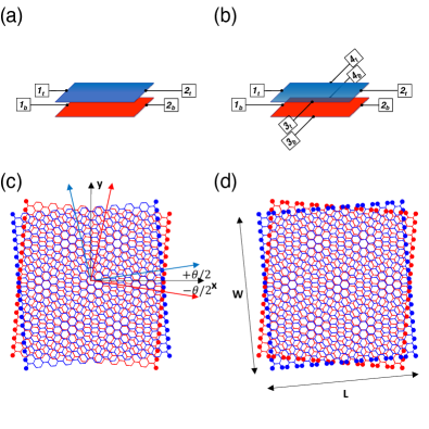
A representation of the studied devices is shown in Fig. 1(a)-(b), it consist of one layer of graphene stacked atop other graphene layer. For positive twist angles, as shown in the figure, the top layer is rotated by and the bottom layer by . For simplicity, in the device presentation, the contact appears at a single site, but in the atomic representation, it is connected to all the outermost atoms at the edges, as shown in the Fig. 1(c)-(d). Unless otherwise specified, we will use a TBG region of dimensions with nm. Initially, we attach the contacts to the zigzag edges of each layer of the central region, creating an armchair TBG nanoribbon. In the second part of the work, we add contacts to the armchair edges of each layer, thus creating a square TBG junction.
The Hamiltonian of the central region () is described by a tight-binding model where the hopping amplitudes between sites and are given by . Here, the bond length , and denotes the angle formed by and the -axis. It is important to note that the hoppings depend on the bond length [44, 45]: and , where , , , , and . Additionally, to accurately describe the electronic properties of TBG, for each site , the neighbors are chosen within a disc of radius .
To calculate the electrical response of the TBG devices, we start with the conductance between contacts and , defined as . In this expression, is the Green’s function of the central region, and represents the self-energy terms, which are four for the TBG nanoribbon and eight for the TBG junction. Regardless of the number of terminals in the device, a wide band model is assumed for all of them. This means that the on-site term , where is the nearest neighbor hopping parameter of graphene [46, 47, 48], is added to all atomic sites where the contacts are attached. These sites are represented in Fig. 1(c)-(d) as filled dots. Equally, for each contact there is broadening function .
II Two-terminal configuration with four contacts
We start with the central square TBG region with layer differentiated leads attached to the source (left) and to the drain (right). The contacts attached to the left top () and bottom () layers are labeled as and , while the contacts attached to the right are designated as and . The layer differentiation allows us to treat the system as four-terminal device with a relation between current and voltages at each terminal as
| (1) |
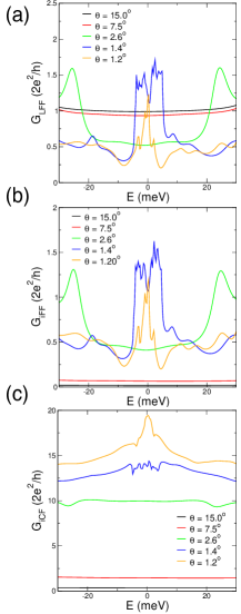
In this expression the current vector is defined as and the voltage vector . The diagonal terms of the conductance matrix are , , ; additionally, it is assumed that . Based on the symmetry of the device, i.e., the same coupling to the leads of the top and bottom layer, only three independent conductance terms define the response matrix: (i) the Layer Forward Flow Conductance , that is related to the probability that one electron injected into one layer exits at the opposite contact of the same layer; (ii) the interlayer Forward Flow Conductance , that is associated with the probability of an electron injected into one layer forward flowing in the opposite layer; (iii) the interlayer Counter Flow Conductance which pertains to the probability of one electron injected into one layer counterflowing in the opposite layer.
In Figs. 2(a)-(c), we can observe the three conductances for different twist angles. For TBG, three coupling regimes between layers can be defined, dictating the lineshape of the conductance.[46, 49, 50] For large angles (), the layers are decoupled, resulting in a plateau at low energies with , while the values of and are low. As the twist angle is reduced (), the coupling intensity increases, reducing and increasing the interlayer conductances such as and . Finally, for small angles, the layers are strongly coupled, with , exhibiting peaks[51, 52, 53] related to the high Density of States (DOS), entering the regime of magic angle[47] when only one peak is observed. Remarkably, display the largest values of around .
II.1 Layer resistance
To examine the layer-resolved response of our TBG device when a current is injected into the bottom (drive) layer, we use the four-probe resistance , which measures the voltage between terminals and when a fixed current is applied between terminals and [34, 35, 36, 37]. Operationally, we set , , and , which enables us to truncate the fourth row and fourth column of the conductance matrix in Eq. 1. [26] Subsequently, the conductance matrix () is inverted to derive the resistance matrix, facilitating the determination of the voltages via
| (2) |
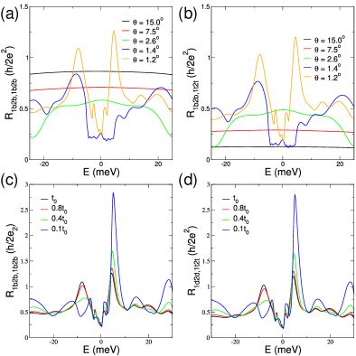
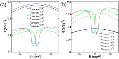
The response of the drive (bottom) layer is accessed by measuring the voltage between the same terminals used to inject the current. From Eqs. 1 and 2, we can write , where is the determinant of . [54, 55]. In Fig. 3(a), the calculated resistance is plotted for different twist angles of the TBG. For large twist angles (), a constant resistance is observed, which decreases as the twist angle increases. For intermediate angles (), the resistance continues to shrink, but some oscillations begin to appear. Finally, for low twist angles (), two broad peaks are observed around the charge neutrality point (CNP). It is worth noting that the layer resistance
| (3) |
depends on various conductance terms, all of which contribute to the effective resistance of the layer.
II.2 Counterflow resistance
The response of the top (drag) layer is assessed by the resistance , which links the voltage drop across the top layer to the current flowing in the bottom layer. In Fig. 3(b), the calculated resistance is plotted for different twist angles of the TBG. Firstly, it is important to mention that the generalized resistance clearly demonstrates a response from the drag layer to the current flow in the drive layer, regardless of the twist angle. Secondly, the resistance calculated for the different angles is always positive. In order to understand this result we have to note that . Or, in other words,
| (4) |
This indicates that the generalized resistance is positive because the counterflow component exceeds the interlayer forward flow. And, it can be concluded that the current in the drag layer flows in the opposite direction to the drive layer. However, the behavior of requires closer examination to determine whether it represents a genuine counterflow throughout the entire top layer or arises from the influence of effective contacts, which may cause significant electron scattering from contact to contact .
Keeping that in mind, the coupling between the contacts and the central TBG region is reduced from the strong coupling regime (calculations presented so far), where the hopping between the contacts and the central region is , to the weak coupling regime with a hopping strength of , where represents the nearest-neighbor hopping energy. Without loss of generality, the effect of coupling reduction on and is shown for the system with in Fig. 3(c) and (d), respectively. While the coupling significantly alters the resistance line shapes, minimizing external influences from the contacts highlights the intrinsic properties of the TBG region, resulting in an increase in drag resistance. Additionally, it is observed that the drive and drag resistances exhibit nearly identical responses. These findings suggest that the counterflow is not caused by scattering at the contacts but rather represents the natural response of the top layer to the current flow in the bottom layer.
III Hall-bar configuration with eight contacts
Having established that a current in the drive layer induces a longitudinal flow in the drag layer, our attention now shifts to exploring the potential for inducing transverse and longitudinal flows. [21, 22, 23, 24, 25] To achieve this, we introduce layer-specific contacts to the armchair edges of TBG. Similar to what was done in the previous case, the relation between the current and voltages at each terminal is determined by the conductance matrix ().
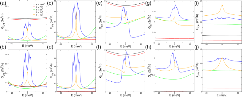
Given the symmetries of the eight-terminal TBG device, out of the elements of the conductance matrix, we have 10 independent terms. Note that despite having a square junction, our system does not possess a fourfold rotational symmetry,[26, 54, 55] which is due to the distinction between the armchair and zigzag directions.[56] Specifically, we have the layer forward zigzag conductance , the layer forward armchair conductance , the counterflow zigzag conductance , the counterflow armchair conductance , the interlayer forward zigzag conductance and the interlayer forward armchair conductance . Similarly to a square junction, we define the layer turn right conductance and the layer turn left conductance . For these definitions, we have used contact as reference, since, as can be observed, a turn to the right in the upper layer, by symmetry, can be a turn to the left in the lower layer. The above is also valid for the interlayer turn right conductance and the interlayer turn left conductance .
In Fig. 4(a)-(j), the independent conductances are presented as a function of energy for different twist angles. Due to the system being completely open, quantum interference is reduced, and the merging of the conductance peaks in the magic-angle regime is evident, see for example the layer and interlayer forward conductances , , and . The three transport schemes defined by the interlayer coupling strength can also be observed, characterized by the increase in interlayer conductances and the decrease of intralayer conductance values when the twist angle is reduced. It is interesting to note that forward conductances are more or less electron-hole symmetric, while those involving some type of turn are asymmetric and exhibit higher values.
III.1 Layer longitudinal resistances
Although the dimensions of the involved matrices increase in the system of eight contacts compared to the one with four, the procedure remains identical. The contact injecting current and the one extracting it are identified. The voltage is set equal to zero for the latter, allowing the corresponding row and column to be eliminated from the conductance matrix. The reduced matrix , with dimensions , is inverted to find the voltages at the other contacts. Based on observations that the forward conductances are different, we have selected two configurations. In the first one, the current is injected and extracted at the zigzag edges of the bottom layer. That is, with , and setting the currents to zero in the remaining contacts. The resistances in this setup are given by , where the contacts and can be any of the remaining six contacts. In the second arrangement, the current is injected and extracted at the armchair edges of the bottom layer and with . The resistances are defined as .
We begin by evaluating the longitudinal resistances of the drive layer and , which entails measuring the voltage using the same terminals that inject the current for both configurations. We find for large angles that there is a constant value, which decreases for small angles, exhibiting dips around the CNP that later merge into one in the magic angle regime. It is interesting to note that, despite the intralayer and interlayer forward conductances being different for armchair and zigzag orientations, the resistances and are very similar. This is evidenced in Fig. 5(a), where we can see that , for the other twist angles, we found a maximum difference of 5% between their values.
The longitudinal resistances of the drag layer ( and ), which link the voltage drop in the armchair and zigzag directions of the top layer, induced by the current in the bottom layer are presented in Fig. 5(d) for some twist angles. We can say first that, similar to the four-contact case, the line shapes are nearly identical to the longitudinal local case. From a general point of view, the values of and increase as the angle decreases, and for small angles, the two dips in the conductance appear, which later merge into one, as can we see. Second, the calculated longitudinal drag resistances values in the two directions, when compared to each other, do not show a difference greater than 5%. Third, for all angles, the values were positive, which means that in the case of , the current injected by contact is more coupled with contact than with contact . And in the case of , the current is more coupled with contact than , allowing us to conclude that in both directions, a counterflow is generated in the drag (top) layer.
III.2 Layer Hall resistances
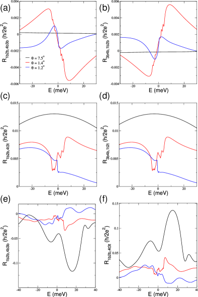
We now focus on examining the accumulation of charge in the transverse direction to the current flow,[23, 25] first in the bottom (drive) layer (, ) and then in the top (drag) layer (, ). As shown in Fig. 6(a)-(b) for the drive layer, although the transverse charge accumulation is small, it increases when reducing the angle. A change in the resistance signal is also observed, indicating that the charge accumulation is reversed when passing through the CNP; this is common for both setups. However, upon comparison, we observe that .
For the drag layer, the Hall resistance is exactly the same in both configurations: , and it is 25 times greater than the Hall resistance of the drive layer, which is noticeable even for large angles, as observed in Figs. 6(c) and (d). We highlight that the direction of the layer Hall voltage can be reversed by changing the twist direction ( and ).
To observe the intrinsic response of TBG, the coupling between the contacts and the central region is reduced. This time, however, the focus is on the Hall response, shown in Figs. 6(e) and (f) for the drive layer () and the drag layer () under a weak coupling of . Notably, the Hall response in both the drive and drag layers increases across all presented angles. The case of (black line) is particularly significant, as the drag Hall resistance reaches the highest values despite the weak interlayer coupling. This aligns with the observation that chiral effects in TBG are more pronounced away from the magic angle [19]. Additionally, it is worth noting that , which, together with the counterflow longitudinal drag resistance, suggests the formation of a circulating current or a magnetic moment induced by the current injected into the bottom layer.
III.3 Disorder and size effects
Up to now, our results for TBG devices with four and eight contacts have demonstrated the induction of longitudinal and transverse open-circuit voltages in the drag layer as a result of an injected current in the drive layer. However, it is well established that mesoscopic current and voltage measurements are both sample-specific and non-local [26, 37]. Considering this, we will investigate the impact of two perturbations. First, we will analyze the effect of onsite disorder on our nm2 sample, followed by an evaluation of the sample size effect using a pristine device with dimensions of nm2.
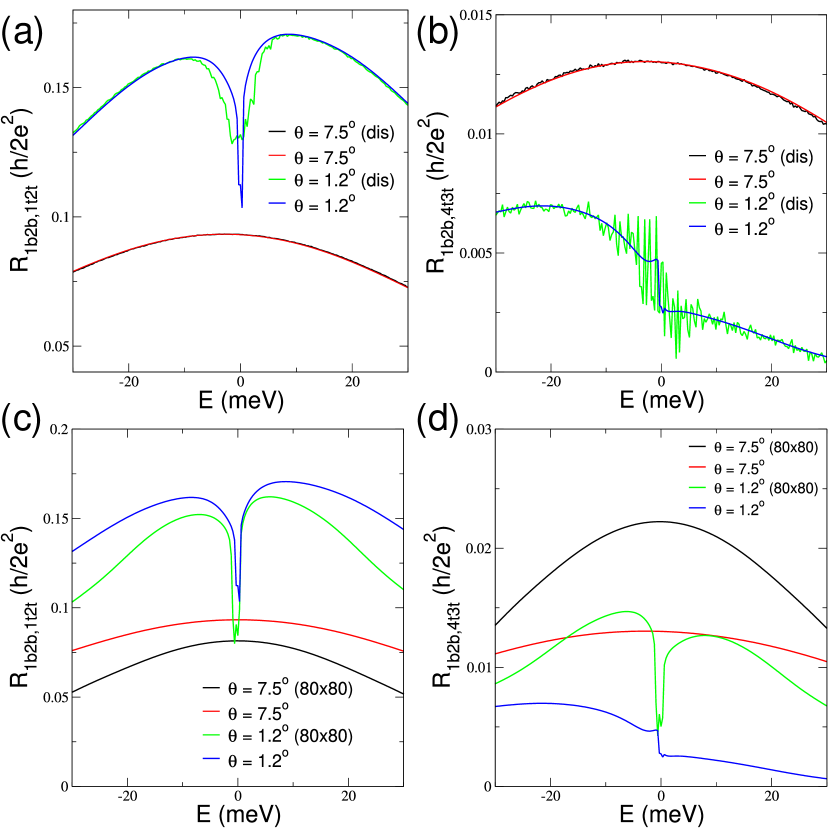
For the disorder case, a low concentration of short-range impurities—occupying 10% of the lattice sites—is randomly introduced by assigning onsite energies selected from a uniform distribution within the range . The conductance matrix elements are averaged over 10 different configurations, and the linear system is then solved to obtain the four-probe resistance. The results are presented in Fig. 7(a) for and in Fig. 7(b) for , indicating that disorder has a minimal impact on the strength of the induced longitudinal and Hall counterflows. For a large twist angle (), the disordered resistance closely resembles that of the pristine case, with both curves nearly overlapping in shape and magnitude. In contrast, for a low twist angle (), the high DOS near the CNP allows electrons to scatter into multiple states with the same energy, leading to a broadening of the dip in or oscillations in . Despite these disorder-induced modifications, the fundamental counterflow behavior remains preserved, reinforcing the robustness of the effect across different disorder configurations and twist angles.
To investigate the effect of the central region’s size, the four-probe resistances were calculated for a TBG device with dimensions , where nm. The longitudinal drag resistance , shown in Fig. 7(c), exhibits a response similar to that of the smaller nm2 device. In contrast, , presented in Fig. 7(d), maintains a comparable strength but displays a different line shape, which is particularly evident for low twist angles. Since our calculations consider fully coherent transport in an entirely open system, electrons in the TBG interact with the entire device, including the highly doped contacts, making it unreasonable to expect identical response shapes [37, 35]. The key takeaway here is that, even in a larger system, the counterflow response remains robust.
IV Machine Learning approach
From the strictly scientific point of view, we have shown the appearance of longitudinal and Hall counterflow in the drag layer. Our analysis relies on the numerical calculation of the conductance matrix using the Green’s function, which is the most computationally intensive part, and its subsequent inversion. With the idea of developing and evaluating new numerical tools to access the transport properties of devices, in this section we show our effort to calculate the four probe resistances of TBG using ML techniques.
The key benefit of using ML is the substantial reduction in computational cost compared to traditional simulations[57, 58, 59], without sacrificing accuracy. Once the ML model is trained, it can quickly compute the individual terms of the conductance matrix (), which are then incorporated into the conventional quantum transport framework to calculate the resistance . This hybrid approach significantly reduces the computation time by addressing the most resource-intensive part of the process. With this in mind the Gradient Boosting Regressor (GBR)[41, 42, 43] was trained, validated, and tested.
To generate inputs for the ML models, over 289,000 samples were collected. Each sample contains the input electrical contact (injection lead), the output electrical contact (extraction lead), the normalized energy, the twist angle, and the normalized conductance. The samples span energy values ranging from approximately meV to 40 meV, with an energy step of 0.3 meV. A total of 18 different twist angles were considered, ranging from to , with a higher density of samples between and . This results in about 13,200 samples for each twist angle in the dataset.
Normalization was applied to standardize their values around a reference point, ensuring a consistent numerical range across all angles and making the input data comparable for the ML models[60]. Specifically, the first normalization was done using Scikit-learn’s StandardScaler [61, 62] function, adjusting the data to have a mean of zero and a standard deviation of one. The second normalization was carried out with the MinMaxScaler [61, 62] function, also from Scikit-learn, scaling the data to a range between zero and one. These steps are essential to ensure that the input variables are comparable in scale and magnitude[62], preventing the models from being unduly influenced by differences in scale [60].
IV.1 Divide-and-conquer
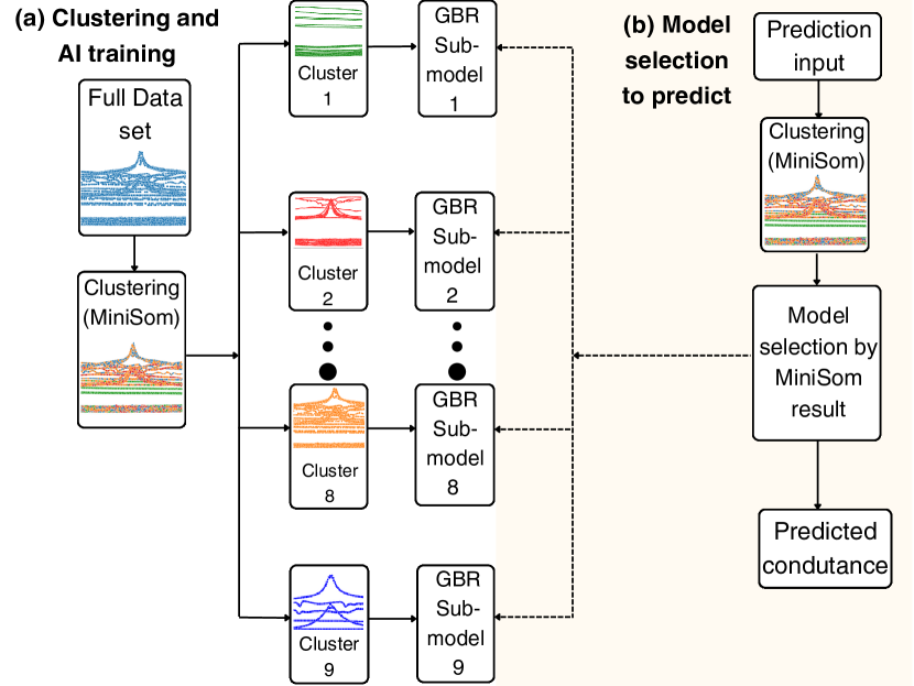
To address the complexity of predicting the 56 off-diagonal elements of the conductance matrix, MiniSom [63, 64] was employed to segment the data into clusters as the first step of a divide-and-conquer strategy. Fig. 8 illustrates the entire process. Initially, the data were segmented into clusters, and then independent GBR submodels were trained for each cluster[65, 66, 67, 68, 69, 70]. This is demonstrated in panel (a) “Clustering and AI Training,” where the segmentation of the data and subsequent training of AI submodels are shown. The second part, in panel (b) “Model Selection to Predict”, details the automated process of selecting the most appropriate submodel for conductance prediction based on the inputs. These inputs are processed by MiniSom, which identifies the corresponding cluster, after which the GBR sub-model trained for that specific cluster is selected to make the prediction.
To identify the optimal number of clusters, we applied two methods: the Akaike Information Criterion (AIC) and the Bayesian Information Criterion (BIC) [71, 61, 72]. These criteria aim to determine the number of clusters that minimize their respective values, ensuring a balance between model simplicity and data fit. Both AIC and BIC were evaluated across a range of 1 to 12 clusters, and notably, both methods identified 9 clusters as the optimal choice.
IV.2 Hyperparameter Tuning, Model Training, and Validation
For each GBR submodel, the tuned hyperparameters include the learning rate (), the number of estimators (), and the maximum tree depth (), as these parameters play a crucial role in shaping the model’s learning and generalization abilities. All other parameters are kept at their default values [73]. The learning rate () determines the impact of each tree on the final prediction, while the number of estimators () specifies the number of boosting stages. Meanwhile, the maximum depth () sets a limit on the number of nodes in each tree, controlling how deep the trees can grow before stopping [73].
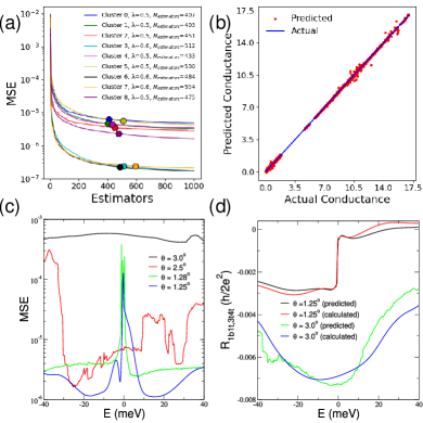
The tuning process is structured into three stages [73]: data preparation, searching for the optimal combination of and , and finally, optimizing tree depth. In the first stage, the dataset is randomly split, with 80% allocated for training and 20% for validation. The second stage involves fixing at 5 while training individual submodels using various combinations of and . To guide hyperparameter selection, the mean squared error (MSE) is computed at each boosting iteration. Training is stopped when the MSE stabilizes or begins to increase, indicating that the model has reached its optimal generalization point before overfitting occurs [61, 73]. It is important to note that, since multiple combinations of (, ) can yield similar MSE values, configurations that achieve low error while minimizing the number of estimators are prioritized [73]. Fig. 9(a) illustrates this process for the nine GBR submodels, where the MSE curves are analyzed to determine for the values shown in the legend. The chosen values for each cluster are represented by colored dots and indicated in the legend. In the third stage, after determining the optimal and , the tree depth is refined by evaluating the MSE for different values ranging from 5 to 20. The guiding principle in this step is to choose the smallest tree depth that minimizes the MSE [73].
The final set of selected hyperparameters is summarized in Table 1. These values define the architecture of the trained GBR submodels, which are subsequently used for conductance predictions. The performance of these predictions on the validation dataset is illustrated in Fig. 9(b), where the blue line represents the actual conductance values, and the red dots indicate the predictions made by the GBR model. The strong agreement between the predicted and actual values confirms that the model effectively captures the underlying physical relationships governing conductance estimation.
As an additional test, we assess the model’s predictive performance for twist angles not present in the training or validation datasets. Fig. 9(c) depicts the MSE, defined as , as a function of energy for these previously excluded twist angles. Here, represents the number of off-diagonal terms, and denotes the conductance predicted () by the GBR model or computed () using Green’s functions. Overall, the observed MSE values remain low, but certain features highlight the strong dependence of transport properties in TBG on the twist angle. For , the black curve stays relatively flat across the energy range, maintaining a higher and nearly constant value. This indicates the absence of significant features or sharp variations in conductance, in contrast to the lower-angle cases, where a pronounced peak at meV emerges due to the high density of states (DOS).
| Cluster | Max Depth | ||
|---|---|---|---|
| 0 | 0.5 | 407 | 10 |
| 1 | 0.5 | 403 | 9 |
| 2 | 0.5 | 451 | 6 |
| 3 | 0.6 | 512 | 15 |
| 4 | 0.5 | 433 | 13 |
| 5 | 0.5 | 508 | 9 |
| 6 | 0.6 | 484 | 10 |
| 7 | 0.4 | 593 | 7 |
| 8 | 0.5 | 475 | 8 |
These predictive limitations are reflected in the four-probe resistance, as shown in Fig. 9(d), where the predicted is compared to the calculated values. For , both curves follow a similar overall trend, featuring a wide dip. However, the predicted resistance appears noisier and alternates between underestimating and overestimating the calculated values across the entire energy range. For , both curves exhibit strong agreement, with the GBR model successfully capturing the step discontinuity around the CNP. From a quantum transport perspective, it is important to emphasize that this resistance has not been previously presented. It was selected both to evaluate the predictive capability of the GBR model and to underscore the complexity of layer-resolved quantum transport phenomena in TBG.
V Final remarks
This work is structured into two main, well-defined yet interconnected sections. The first section presents and analyzes the layer-resolved quantum transport response of TBG using a traditional method. The second section, which relies heavily on data generated from Green’s functions, introduces a novel divide-and-conquer ML approach to compute all elements of the conductance matrix. Together, this work advances our understanding of quantum transport in TBG and provide innovative tools for studying transport in twisted devices.
In the first part, we calculated the conductance and then determined the four-probe resistance of TBG devices with four and eight-layer differentiated contacts. For a TBG nanoribbon geometry with only four-layer differentiated contacts, our results reveal the emergence of a current counterflow in the top layer when current is injected into the bottom layer. In the square junction configuration, i.e., a TBG device with eight-layer specific contacts, the longitudinal counterflow is accompanied by a transverse or Hall counterflow when the current flows longitudinally in the bottom layer. These observations remain consistent despite weak interactions with the contacts, onsite disorder, and the device size. Notably, the counterflow response indicates a circulating current between layers, or in other words, the formation of an in-plane magnetic moment, induced by the injected current. Our findings demonstrate how to detect this in-plane magnetic moment using electrical measurements.
In the second part of our manuscript, we demonstrate that ML models can be integrated into the quantum transport algorithm to accelerate calculations. While this approach itself is not novel, the significant variations in conductance as a function of the twist angle allowed for the successful implementation of a novel divide-and-conquer strategy. Our predictive system, consisting of specialized GBR submodels for each cluster, enables more accurate and efficient predictions. However, the proposed ML model faced challenges in accurately predicting conductance for certain twist angles, highlighting the need for additional training data or more refined ML models to enhance precision. In this context, we also trained, validated, and tested Multi-Layer Perceptron (MLP) [74, 75, 76] and Support Vector Regression (SVR) [77, 78, 79] for the nine clusters, but GBR demonstrated the best performance. The trained GBR model and the instructions to run it are available [80].
Acknowledgments
M.H.G.K. gratefully acknowledges CAPES-PROSUC (88882.462011/2019-01) and the high-performance computing cluster of the Mackenzie Presbyterian University (https://mackcloud.mackenzie.br). D.A.B. acknowledges support from the Brazilian Nanocarbon Institute of Science and Technology (INCT/Nanocarbon), CAPES-PRINT (grants nos. 88887.310281/2018-00 and 88887.899997/2023-00), CNPq (309835/2021-6), and Mackpesquisa. D.A.B. also thanks Tobias Stauber and Guillermo Gómez-Santos for bringing this topic to his attention and for their valuable feedback on the initial version of the manuscript.
References
- Andrei et al. [2021] E. Y. Andrei, D. K. Efetov, P. Jarillo-Herrero, A. H. MacDonald, K. F. Mak, T. Senthil, E. Tutuc, A. Yazdani, and A. F. Young, The marvels of moirématerials, Nature Reviews Materials 6, 201 (2021).
- He et al. [2021] F. He, Y. Zhou, Z. Ye, S.-H. Cho, J. Jeong, X. Meng, and Y. Wang, Moiré patterns in 2d materials: A review, ACS Nano 15, 5944 (2021), pMID: 33769797, https://doi.org/10.1021/acsnano.0c10435 .
- Bernevig and Efetov [2024] B. A. Bernevig and D. K. Efetov, Twisted bilayer graphene’s gallery of phases, Physics Today 77, 38 (2024), https://pubs.aip.org/physicstoday/article-pdf/77/4/38/19858215/38_1_pt.jvsd.yhyd.pdf .
- Cao et al. [2018a] Y. Cao, V. Fatemi, A. Demir, S. Fang, S. L. Tomarken, J. Y. Luo, J. D. Sanchez-Yamagishi, K. Watanabe, T. Taniguchi, E. Kaxiras, R. C. Ashoori, and P. Jarillo-Herrero, Correlated insulator behaviour at half-filling in magic-angle graphene superlattices, Nature 556, 80 EP (2018a).
- Cao et al. [2018b] Y. Cao, V. Fatemi, S. Fang, K. Watanabe, T. Taniguchi, E. Kaxiras, and P. Jarillo-Herrero, Unconventional superconductivity in magic-angle graphene superlattices, Nature 556, 43 EP (2018b).
- Cao et al. [2020a] Y. Cao, D. Chowdhury, D. Rodan-Legrain, O. Rubies-Bigorda, K. Watanabe, T. Taniguchi, T. Senthil, and P. Jarillo-Herrero, Strange metal in magic-angle graphene with near planckian dissipation, Phys. Rev. Lett. 124, 076801 (2020a).
- Zhang et al. [2019] Y.-H. Zhang, D. Mao, Y. Cao, P. Jarillo-Herrero, and T. Senthil, Nearly flat chern bands in moiré superlattices, Phys. Rev. B 99, 075127 (2019).
- Cao et al. [2020b] Y. Cao, D. Rodan-Legrain, O. Rubies-Bigorda, J. M. Park, K. Watanabe, T. Taniguchi, and P. Jarillo-Herrero, Tunable correlated states and spin-polarized phases in twisted bilayer–bilayer graphene, Nature 583, 215 (2020b).
- Park et al. [2021] J. M. Park, Y. Cao, K. Watanabe, T. Taniguchi, and P. Jarillo-Herrero, Tunable strongly coupled superconductivity in magic-angle twisted trilayer graphene, Nature 590, 249 (2021).
- Lin et al. [2022] J.-X. Lin, P. Siriviboon, H. D. Scammell, S. Liu, D. Rhodes, K. Watanabe, T. Taniguchi, J. Hone, M. S. Scheurer, and J. I. A. Li, Zero-field superconducting diode effect in small-twist-angle trilayer graphene, Nature Physics 18, 1221 (2022).
- Scammell et al. [2022] H. D. Scammell, J. I. A. Li, and M. S. Scheurer, Theory of zero-field superconducting diode effect in twisted trilayer graphene, 2D Materials 9, 025027 (2022).
- Liu et al. [2020] X. Liu, Z. Hao, E. Khalaf, J. Y. Lee, Y. Ronen, H. Yoo, D. Haei Najafabadi, K. Watanabe, T. Taniguchi, A. Vishwanath, and P. Kim, Tunable spin-polarized correlated states in twisted double bilayer graphene, Nature 583, 221 (2020).
- Wang et al. [2020] L. Wang, E.-M. Shih, A. Ghiotto, L. Xian, D. A. Rhodes, C. Tan, M. Claassen, D. M. Kennes, Y. Bai, B. Kim, K. Watanabe, T. Taniguchi, X. Zhu, J. Hone, A. Rubio, A. N. Pasupathy, and C. R. Dean, Correlated electronic phases in twisted bilayer transition metal dichalcogenides, Nature Materials 19, 861 (2020).
- Ghiotto et al. [2021] A. Ghiotto, E.-M. Shih, G. S. S. G. Pereira, D. A. Rhodes, B. Kim, J. Zang, A. J. Millis, K. Watanabe, T. Taniguchi, J. C. Hone, L. Wang, C. R. Dean, and A. N. Pasupathy, Quantum criticality in twisted transition metal dichalcogenides, Nature 597, 345 (2021).
- Xu et al. [2022] Y. Xu, K. Kang, K. Watanabe, T. Taniguchi, K. F. Mak, and J. Shan, A tunable bilayer hubbard model in twisted wse2, Nature Nanotechnology 17, 934 (2022).
- Li et al. [2024] H. Li, Z. Xiang, M. H. Naik, W. Kim, Z. Li, R. Sailus, R. Banerjee, T. Taniguchi, K. Watanabe, S. Tongay, A. Zettl, F. H. da Jornada, S. G. Louie, M. F. Crommie, and F. Wang, Imaging moiréexcited states with photocurrent tunnelling microscopy, Nature Materials 23, 633 (2024).
- Wang et al. [2022] P. Wang, G. Yu, Y. H. Kwan, Y. Jia, S. Lei, S. Klemenz, F. A. Cevallos, R. Singha, T. Devakul, K. Watanabe, T. Taniguchi, S. L. Sondhi, R. J. Cava, L. M. Schoop, S. A. Parameswaran, and S. Wu, One-dimensional luttinger liquids in a two-dimensional moirélattice, Nature 605, 57 (2022).
- Anderson et al. [2023] E. Anderson, F.-R. Fan, J. Cai, W. Holtzmann, T. Taniguchi, K. Watanabe, D. Xiao, W. Yao, and X. Xu, Programming correlated magnetic states with gate-controlled moiré geometry, Science 381, 325 (2023), https://www.science.org/doi/pdf/10.1126/science.adg4268 .
- Kim et al. [2016] C.-J. Kim, S.-C. A., Z. Ziegler, Y. Ogawa, C. Noguez, and J. Park, Chiral atomically thin films, Nat. Nanotechnol. 11, 520 (2016).
- Morell et al. [2017] E. S. Morell, L. Chico, and L. Brey, Twisting dirac fermions: circular dichroism in bilayer graphene, 2D Materials 4, 035015 (2017).
- Stauber et al. [2018] T. Stauber, T. Low, and G. Gómez-Santos, Chiral response of twisted bilayer graphene, Phys. Rev. Lett. 120, 046801 (2018).
- Bistritzer and MacDonald [2011] R. Bistritzer and A. H. MacDonald, Moiré bands in twisted double-layer graphene, P. Natl. Acad. Sci. Usa. 108, 12233 (2011).
- Zhai et al. [2023] D. Zhai, C. Chen, C. Xiao, and W. Yao, Time-reversal even charge hall effect from twisted interface coupling, Nature Communications 14, 1961 (2023).
- Guerci et al. [2021] D. Guerci, P. Simon, and C. Mora, Moiré lattice effects on the orbital magnetic response of twisted bilayer graphene and condon instability, Phys. Rev. B 103, 224436 (2021).
- Ding and Zhao [2023] C. Ding and M. Zhao, Chiral response in two-dimensional bilayers with time-reversal symmetry: A universal criterion, Phys. Rev. B 108, 125415 (2023).
- Datta [1995] S. Datta, Electronic Transport in Mesoscopic Systems (Cambridge University Press, 1995).
- Ferry and Goodnick [1997] D. Ferry and S. M. Goodnick, Transport in Nanostructures, Cambridge Studies in Semiconductor Physics and Microelectronic Engineering (Cambridge University Press, 1997).
- Gorbachev et al. [2012] R. V. Gorbachev, A. K. Geim, M. I. Katsnelson, K. S. Novoselov, T. Tudorovskiy, I. V. Grigorieva, A. H. MacDonald, S. V. Morozov, K. Watanabe, T. Taniguchi, and L. A. Ponomarenko, Strong coulomb drag and broken symmetry in double-layer graphene, Nature Physics 8, 896 (2012).
- Liu et al. [2017a] X. Liu, K. Watanabe, T. Taniguchi, B. I. Halperin, and P. Kim, Quantum hall drag of exciton condensate in graphene, Nature Physics 13, 746 (2017a).
- Sanchez-Yamagishi et al. [2017] J. D. Sanchez-Yamagishi, J. Y. Luo, A. F. Young, B. M. Hunt, K. Watanabe, T. Taniguchi, R. C. Ashoori, and P. Jarillo-Herrero, Helical edge states and fractional quantum hall effect in a graphene electron–hole bilayer, Nature Nanotechnology 12, 118 (2017).
- Liu et al. [2019] X. Liu, Z. Hao, K. Watanabe, T. Taniguchi, B. I. Halperin, and P. Kim, Interlayer fractional quantum hall effect in a coupled graphene double layer, Nature Physics 15, 893 (2019).
- Liu et al. [2022] X. Liu, J. I. A. Li, K. Watanabe, T. Taniguchi, J. Hone, B. I. Halperin, P. Kim, and C. R. Dean, Crossover between strongly coupled and weakly coupled exciton superfluids, Science 375, 205 (2022), https://www.science.org/doi/pdf/10.1126/science.abg1110 .
- Liu et al. [2017b] X. Liu, L. Wang, K. C. Fong, Y. Gao, P. Maher, K. Watanabe, T. Taniguchi, J. Hone, C. Dean, and P. Kim, Frictional magneto-coulomb drag in graphene double-layer heterostructures, Phys. Rev. Lett. 119, 056802 (2017b).
- Timp et al. [1988] G. Timp, H. U. Baranger, P. deVegvar, J. E. Cunningham, R. E. Howard, R. Behringer, and P. M. Mankiewich, Propagation around a bend in a multichannel electron waveguide, Phys. Rev. Lett. 60, 2081 (1988).
- Büttiker [1986] M. Büttiker, Four-terminal phase-coherent conductance, Phys. Rev. Lett. 57, 1761 (1986).
- Beenakker and van Houten [1991] C. Beenakker and H. van Houten, Quantum transport in semiconductor nanostructures, in Semiconductor Heterostructures and Nanostructures, Solid State Physics, Vol. 44, edited by H. Ehrenreich and D. Turnbull (Academic Press, 1991) pp. 1–228.
- Stone and Szafer [1988] S. D. Stone and A. Szafer, What is measured when you measure a resistance?—the landauer formula revisited, IBM J. Res. Dev. 32, 384–413 (1988).
- Piccinotti et al. [2020] D. Piccinotti, K. F. MacDonald, S. A. Gregory, I. Youngs, and N. I. Zheludev, Artificial intelligence for photonics and photonic materials, Reports on Progress in Physics 84, 012401 (2020).
- Ma et al. [2021] W. Ma, Z. Liu, Z. A. Kudyshev, A. Boltasseva, W. Cai, and Y. Liu, Deep learning for the design of photonic structures, Nature Photonics 15, 77 (2021).
- Jiang et al. [2021] J. Jiang, M. Chen, and J. A. Fan, Deep neural networks for the evaluation and design of photonic devices, Nature Reviews Materials 6, 679 (2021).
- Wade and Glynn [2020] C. Wade and K. Glynn, Hands-On Gradient Boosting with XGBoost and scikit-learn: Perform accessible machine learning and extreme gradient boosting with Python (Packt Publishing Ltd, 2020).
- Friedman [2001] J. H. Friedman, Greedy function approximation: A gradient boosting machine, Annals of Statistics , 1189 (2001).
- Prettenhofer and Louppe [2014] P. Prettenhofer and G. Louppe, Gradient boosted regression trees in scikit-learn, in PyData 2014 (2014).
- Brihuega et al. [2012] I. Brihuega, P. Mallet, H. González-Herrero, G. Trambly de Laissardière, M. M. Ugeda, L. Magaud, J. M. Gómez-Rodríguez, F. Ynduráin, and J.-Y. Veuillen, Unraveling the intrinsic and robust nature of van hove singularities in twisted bilayer graphene by scanning tunneling microscopy and theoretical analysis, Phys. Rev. Lett. 109, 196802 (2012).
- Moon and Koshino [2012] P. Moon and M. Koshino, Energy spectrum and quantum hall effect in twisted bilayer graphene, Phys. Rev. B 85, 195458 (2012).
- Bahamon et al. [2020] D. A. Bahamon, G. Gómez-Santos, and T. Stauber, Emergent magnetic texture in driven twisted bilayer graphene, Nanoscale 12, 15383 (2020).
- Bahamon et al. [2024] D. A. Bahamon, G. Gómez-Santos, D. K. Efetov, and T. Stauber, Chirality probe of twisted bilayer graphene in the linear transport regime, Nano Letters 24, 4478 (2024), pMID: 38584591, https://doi.org/10.1021/acs.nanolett.4c00371 .
- Bahamon et al. [2013] D. A. Bahamon, A. H. Castro Neto, and V. M. Pereira, Effective contact model for geometry-independent conductance calculations in graphene, Phys. Rev. B 88, 235433 (2013).
- de Castro et al. [2024] S. G. de Castro, J. a. M. V. P. Lopes, A. Ferreira, and D. A. Bahamon, Fast fourier-chebyshev approach to real-space simulations of the kubo formula, Phys. Rev. Lett. 132, 076302 (2024).
- de Castro et al. [2023] S. G. de Castro, A. Ferreira, and D. A. Bahamon, Efficient chebyshev polynomial approach to quantum conductance calculations: Application to twisted bilayer graphene, Phys. Rev. B 107, 045418 (2023).
- Hou et al. [2024] Z. Hou, Y.-Y. Hu, and G.-W. Yang, Moiré pattern assisted commensuration resonance in disordered twisted bilayer graphene, Phys. Rev. B 109, 085412 (2024).
- Sanjuan Ciepielewski et al. [2022] A. Sanjuan Ciepielewski, J. Tworzydło, T. Hyart, and A. Lau, Transport signatures of van hove singularities in mesoscopic twisted bilayer graphene, Phys. Rev. Res. 4, 043145 (2022).
- Ciepielewski et al. [2024] A. S. Ciepielewski, J. Tworzydło, T. Hyart, and A. Lau, Transport effects of twist-angle disorder in mesoscopic twisted bilayer graphene, arXiv preprint arXiv:2403.19313 (2024).
- Baranger et al. [1991] H. U. Baranger, D. P. DiVincenzo, R. A. Jalabert, and A. D. Stone, Classical and quantum ballistic-transport anomalies in microjunctions, Phys. Rev. B 44, 10637 (1991).
- Shepard et al. [1992] K. L. Shepard, M. L. Roukes, and B. P. van der Gaag, Experimental measurement of scattering coefficients in mesoscopic conductors, Phys. Rev. B 46, 9648 (1992).
- Qiao et al. [2011] Z. Qiao, J. Jung, Q. Niu, and A. H. MacDonald, Electronic highways in bilayer graphene, Nano Letters 11, 3453 (2011), pMID: 21766817, https://doi.org/10.1021/nl201941f .
- Torres et al. [2019] V. Torres, P. Silva, E. A. T. de Souza, L. A. Silva, and D. A. Bahamon, Valley notch filter in a graphene strain superlattice: Green’s function and machine learning approach, Phys. Rev. B 100, 205411 (2019).
- Nedell et al. [2022] J. G. Nedell, J. Spector, A. Abbout, M. Vogl, and G. A. Fiete, Deep learning of deformation-dependent conductance in thin films: Nanobubbles in graphene, Phys. Rev. B 105, 075425 (2022).
- Kucukbas et al. [2022] M. E. Kucukbas, S. McCann, and S. R. Power, Predicting magnetic edge behavior in graphene using neural networks, Phys. Rev. B 106, L081411 (2022).
- Hastie et al. [2009] T. Hastie, R. Tibshirani, and J. Friedman, The Elements of Statistical Learning: Data Mining, Inference, and Prediction, 2nd ed., Springer Series in Statistics (Springer New York, 2009).
- Pedregosa et al. [2011] F. Pedregosa, G. Varoquaux, A. Gramfort, V. Michel, B. Thirion, O. Grisel, M. Blondel, P. Prettenhofer, R. Weiss, V. Dubourg, et al., Scikit-learn: Machine learning in python, the Journal of machine Learning research 12, 2825 (2011).
- Jo [2019] J.-M. Jo, Effectiveness of normalization pre-processing of big data to the machine learning performance, The Journal of the Korea Institute of Electronic Communication Sciences 14, 547 (2019).
- Vettigli [2018] G. Vettigli, Minisom: minimalistic and numpy-based implementation of the self organizing map (2018).
- Kohonen [1990] T. Kohonen, The self-organizing map, Proceedings of the IEEE 78, 1464 (1990).
- Trivedi et al. [2015] S. Trivedi, Z. A. Pardos, and N. T. Heffernan, The utility of clustering in prediction tasks, arXiv preprint arXiv:1509.06163 (2015).
- Li et al. [2023] M. Li, Y. Zhu, Y. Shen, and M. Angelova, Clustering-enhanced stock price prediction using deep learning, World Wide Web 26, 207 (2023).
- Bini and Mathew [2016] B. Bini and T. Mathew, Clustering and regression techniques for stock prediction, Procedia Technology 24, 1248 (2016), international Conference on Emerging Trends in Engineering, Science and Technology (ICETEST - 2015).
- Laasonen [2005] K. Laasonen, Clustering and prediction of mobile user routes from cellular data, in Knowledge Discovery in Databases: PKDD 2005: 9th European Conference on Principles and Practice of Knowledge Discovery in Databases, Porto, Portugal, October 3-7, 2005. Proceedings (Springer, 2005) pp. 569–576.
- Teeraratkul et al. [2017] T. Teeraratkul, D. O’Neill, and S. Lall, Shape-based approach to household electric load curve clustering and prediction, IEEE Transactions on Smart Grid 9, 5196 (2017).
- Cherif et al. [2011] A. Cherif, H. Cardot, and R. Boné, Som time series clustering and prediction with recurrent neural networks, Neurocomputing 74, 1936 (2011).
- Sowan et al. [2023] B. Sowan, T.-P. Hong, A. Al-Qerem, M. Alauthman, and N. Matar, Ensembling validation indices to estimate the optimal number of clusters, Applied Intelligence 53, 9933 (2023).
- Bulteel et al. [2013] K. Bulteel, T. F. Wilderjans, F. Tuerlinckx, and E. Ceulemans, Chull as an alternative to aic and bic in the context of mixtures of factor analyzers, Behavior Research Methods 45, 782 (2013).
- Natekin and Knoll [2013] A. Natekin and A. Knoll, Gradient boosting machines, a tutorial, Frontiers in Neurorobotics 7, 10.3389/fnbot.2013.00021 (2013).
- Taud and Mas [2018] H. Taud and J.-F. Mas, Multilayer perceptron (mlp), in Geomatic Approaches for Modeling Land Change Scenarios (Springer, Cham, 2018) pp. 451–455.
- Tang et al. [2015] J. Tang, C. Deng, and G.-B. Huang, Extreme learning machine for multilayer perceptron, IEEE Transactions on Neural Networks and Learning Systems 27, 809 (2015).
- Popescu et al. [2009] M.-C. Popescu, V. E. Balas, L. Perescu-Popescu, and N. Mastorakis, Multilayer perceptron and neural networks, WSEAS Transactions on Circuits and Systems 8, 579 (2009).
- Awad and Khanna [2015] M. Awad and R. Khanna, Support vector regression, in Efficient Learning Machines: Theories, Concepts, and Applications for Engineers and System Designers (Apress, Berkeley, CA, 2015) pp. 67–80.
- Smola and Schölkopf [2004] A. J. Smola and B. Schölkopf, A tutorial on support vector regression, Statistics and Computing 14, 199 (2004).
- Brereton and Lloyd [2010] R. G. Brereton and G. R. Lloyd, Support vector machines for classification and regression, Analyst 135, 230 (2010).
- [80] https://github.com/MatheusHGK/GBR_TBG.