Effects of antiferromagnetic coupling and pinning on domain wall dynamics in synthetic ferrimagnets
Abstract
Domain wall (DW) dynamics in antiferromagnetic (AFM) systems offer the advantages over their ferromagnetic counterparts of having faster and more energy efficient manipulation due to the absence of net magnetization, leading to reduced magnetic crosstalk and improved performance in spintronic devices. A comprehensive analysis of DW dynamics across regimes such as creep, depinning, and flow is well established in ferromagnetic systems but remains lacking in AFM-coupled systems. In this study, we explore the nature of DW dynamics in synthetic ferrimagnetic multilayers composed of PtCoTbAl for different Tb thickness, focusing on the underlying pinning parameters, and on the different regimes of DW dynamics driven by spin-orbit torques (SOTs). We find that due to the AFM coupling between Co and Tb, the magnetic moment of Tb increases with Tb thickness resulting in a reduced saturation magnetization and an enhanced depinning field. The DW disorder interaction is found to vary weakly with the AFM coupling between Co and Tb, while the complete withdrawal of the Tb layer strongly increases the anisotropy and the DW pinning. Furthermore, we propose a novel approach to measure effective SOTs by comparing depinning transitions in current- and field-induced DW motion. This research reveals new insights into DW dynamics in coupled AFM systems, highlighting enhancements in mobility through optimized SOTs and pinning landscapes.
I INTRODUCTION
Controlling the motion of magnetic domain walls (DWs) is crucial for understanding and manipulating the magnetic properties and spintronic behavior of devices in a wide range of applications, such as data storage, logic elements, sensing, and neuromorphic computing [1, 2, 3, 4]. The performance and reliability of DW-based devices are inherently tied to the speed of DW motion, as enhanced mobility reduces the energy cost and facilitates the read and write operation [5, 6, 7]. A first way to move DWs is through torques generated by external magnetic field pulses. In this case, the efficiency of DW motion, notably in the lower range of field amplitude, primarily depends on the pinning landscape as it might induce DW roughness, deformation and stochasticity of motion [8, 9, 10]. The material-specific structural and magnetic properties lead to variations in DW elastic energies and random pinning characteristics across different systems [11, 10, 12]. Although these differences exist, it has been demonstrated that the creep and depinning dynamics of DWs exhibit universal behavior in ferromagnetic materials [9, 13, 14].
Recent proposals advocate for using antiferromagnetic (AFM) materials to boost the DW velocity due to the complete suppression of the angular precession [5, 15, 16, 17]. However, unlike the ferromagnets, the behaviour of the various dynamical regimes for DW dynamics, i.e. creep, depinning, and flow [18, 19, 20] remains poorly understood for antiferromagnets. Additionally, manipulating magnetic textures and DWs in AFM materials is known to be challenging due to their immunity to external magnetic fields [21, 22]. Ferrimagnets, on the other hand, present a significant advantage: they have reduced magnetization and angular momentum like AFMs, but retain control mechanisms similar to ferromagnets due to their non-zero magnetization and near-metallic properties [23, 24, 25]. In this context, our approach has been to examine an uncompensated antiferromagnetically coupled bilayer, which behaves as a synthetic ferrimagnetic system to understand the impact of AFM coupling on DW motion and pinning.
Another approach to moving DWs is through current induced spin torques, specifically the classical spin transfer effects in magnetic tunnel junction (MTJ) [26] or more recently the spin-orbit torques [27, 3, 28, 29]. Simultaneously enhancing the spin torques and reducing the pinning is essential for achieving efficient current-driven DW motion. To address this, we investigate the DW dynamics in a transition metal (TM) - rare earth (RE) multilayer, namely PtCoTbAl, which forms a synthetic ferrimagnetic heterostructure [30]. By carefully balancing the magnetic moments of the Co and Tb layers, we achieve enhanced DW velocity in the creep regime. The insertion of the Tb layer reduces the anisotropy of PtCoAl-based multilayers, thereby decreasing the DW pinning energy and increasing the pinning length. By comparing field- and current-driven DW motion, we demonstrate that the efficiency of the spin torque can be accurately estimated in these systems.
II Sample description & experimental methods
The samples investigated were grown at room temperature on thermally oxidized Si substrates in a high-vacuum sputtering chamber with a base pressure of mbar. The multilayered samples have the following structure: Ta (5 nm)Pt (5 nm)[Pt (3 nm)Co()Tb()Al(3 nm)]×NPt(2 nm), where nm for single repetition, i.e. (denoted SL in the following), and 1.3 nm for (denoted ML), nm, indicates the thermally oxidized Si substrate, covered by 280 nm of SiO2. All the multilayers were grown on top of Ta (5 nm)Pt (8 nm) buffers to help stabilizing perpendicular magnetic anisotropy (PMA) in Co and capped with 2 nm Pt to protect from oxidation. It is worth noting that the thickness of a single atomic layer of Tb is about 0.36 nm. To facilitate the comparison with a ferromagnetic system, we also prepared a single-layer sample without any Tb layer with the following structure: Ta (5 nm)Pt (8 nm)Co(1 nm)Al(3 nm)Pt(2 nm) labeled in the following as PtCoAl. The growth rates of the layers have been calibrated using x-ray reflectivity measurements. The magnetic moment of the individual layers was quantified by performing x-ray magnetic circular dichroism (XMCD) measurements (on DEIMOS beamline at SOLEIL synchrotron, France [31]) at 300 K and 2 T across the and edges of Co and Tb, respectively. The amplitude of the interfacial Dzyaloshinskii–Moriya interaction (i-DMI) in this system was estimated by Brillouin light scattering (BLS) experiments in Damon-Eshbach geometry [32]. The field induced dynamics of the DWs was imaged using a Kerr microscope equipped with a micro-coil placed beneath the sample to provide external magnetic field pulses [33]. For current induced dynamics of the DWs was studied using magnetic force microscopy (MFM) measurements to image sequences of DW displacements after 10-ns long current pulses of varying amplitude. The presence of metallic Tb down to its smallest thickness was confirmed through X-ray photoelectron spectroscopy (XPS) measurements. The stability of the oxygen-sensitive Tb was validated by ensuring consistent data reproducibility over the course of time across multiple measurements.
III Results & Discussion
III.1 Magnetization and Tb thickness
| (nm) | (kA m-1) | (mT) | (kJ m-3) | (kJ m-3) | (K) | (mT) | (m s-1) |
|---|---|---|---|---|---|---|---|
| 0 (SL) | 1150 120 | 1800 90 | 1870 230 | 1040 120 | 11000 1000 | 250 20 | 100 20 |
| 0.25 (SL) | 1020 100 | 730 40 | 1030 130 | 370 40 | 7800 1000 | 55 5 | 70 10 |
| 0.50 (SL) | 820 80 | 1030 50 | 850 100 | 420 50 | 6800 1000 | 90 5 | 80 10 |
| 0.75 (SL) | 630 60 | 1390 70 | 690 90 | 440 50 | 8000 1000 | 170 10 | 115 10 |
| 1.00 (SL) | 500 50 | 1820 90 | 610 70 | 450 50 | 8500 1000 | 170 10 | 115 10 |
| 0.25 (ML) | 990 80 | 480 30 | 860 110 | 240 30 | |||
| 0.50 (ML) | 930 50 | 510 30 | 810 100 | 240 30 | |||
| 0.75 (ML) | 620 60 | 1010 50 | 690 90 | 360 40 | 6500 1000 | 115 10 | 130 10 |
| 1.00 (ML) | 430 30 | 1370 70 | 610 80 | 400 40 | 7000 1000 | 120 10 | 125 10 |
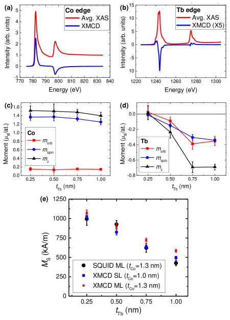
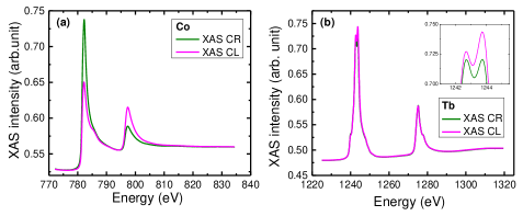
The quantitative estimation of the spin and orbital moments of the individual magnetic elements present in the samples have been obtained by XMCD measurements at 300 K and T at the and edges of Co and Tb, respectively. A detailed procedure for the normalization and background correction of the X-ray absorption spectroscopy (XAS) raw data is provided in Appendix A. In Fig.1(a) and (b), we show the normalized, background corrected, averaged (left and right circular polarization and positive and negative out-of-plane fields) XAS spectra (red curve) along with the XMCD signal (blue curve) at the Co and Tb edges. The opposite sign of the XMCD spectra for the two atoms confirms the anti-parallel arrangement of the Co and Tb magnetic moments. We quantify the spin () and orbital () atomic magnetic moments for Tb and Co, using the so-called XMCD sum rules [34, 35, 36, 37]:
| (1) | |||
| (2) |
The XAS intensities are integrated around the energy edge for Co ( for Tb), or around both and ( and ), defining the values , and for Co or Tb. or index corresponds to the sign of the product of the field by the circular polarization, and equivalent XAS are averaged: , and . The other parameters are , , ; =6, and =2.5, as given by the literature [36, 38, 39].
The extracted atomic spin and orbital moments for both Co and Tb layers are plotted as a function of in Fig.1(c) and (d). In Fig. 1(e), we compare the evolution of the magnetization estimated from XMCD measurements with the one from SQUID measurements. The following equation has been used to obtain the spontaneous magnetization (measured at a field of 2 T saturating domains, but still below the AFM coupling field) determined from the XMCD moments:
| (3) |
where m3 and m3 are the atomic volumes of Co and Tb, and and are the magnetic moments of Co and Tb. It can be seen in Fig. 1(e) that these two independent measurements display a nearly equal evolution of with . This validation is essential, as the accuracy of is crucial for calculating the effective spin Hall angle (), which will be discussed later in section III-C. As expected, in Fig.1(c), the component dominates over in Co due to the significant contribution of the orbitals to its magnetism. We note that the total moment of Co for the lowest nm is whereas for a similar Co film without any Tb layer (sample PtCoAl) is . Furthermore, the Co moment decreases from to with the increase of to nm. The decrease in the Co moment can be understood through the discontinuous environment model [40]. According to this model, the magnetic moment of a TM atom is either zero or maximal, based on the number of surrounding transition metal (TM) atoms. As the probability of Tb atoms surrounding a Co atom increases with increasing , the average magnetic moment of Co atoms effectively decreases. This explanation also holds true in the absence of Tb atoms, when Co atoms are only surrounded by Al atoms. In this case, we observe a magnetic moment of , which is slightly lower than the expected for bulk Co. However, the decrease in Co moment near a Tb atom is stronger than for Al atoms, possibly due to fact that RE and TM elements are extremely prone to alloy formation [41, 42].
Regarding Tb, the magnetic moment increases with . The orbital moment is equivalent to in Tb due to partially filled orbitals. Interestingly, the increase of both Tb spin and orbital moments saturates between and nm. It is important to note that at room temperature, Tb atoms are supposed to be non-magnetic, in contrast to our observation when they are in contact with Co atoms. The mixing between the two species is localised at the interface in such ferrimagnetic multilayers, which explains the saturation of the Tb magnetic moment beyond nm [Fig.1(d)]. This observation is further supported by the relatively low total magnetic moment of Tb in our samples, measuring , compared to the ones reported for TbCo alloys () [36]. As a combination, the total magnetization () of the samples decreases with the increase of .
A detailed summary of the various micromagnetic parameters of the samples (extracted from M-H loops measured using AGFM, and SQUID magnetometry), viz. spontaneous magnetization (), anisotropy field (), uniaxial anisotropy (), and effective anisotropy () is provided in Table 1, where . We note that, as explained by the XMCD data, there is a continuous decrease in with increasing owing to the AFM coupling. For , and , we observe a sharp decrease from to 0.25 nm. This suggests that the interface anisotropy of CoAl is larger than that of CoTb, due to the detailed electronic reconstruction at the CoAl interface [43, 44, 45]. It should be noticed that there is a monotonic decrease (increase) of () in the thickness range of from 0.25 to 1 nm due to the increase in the magnetic compensation while maintaining the same exchange coupling. However, the change in anisotropy energy is less pronounced since it depends on the product of and . Assuming the exchanges (symmetric and antisymmetric ) constant for all the samples, this is expected to result in a strong decrease of the DW energy () and increase of DW width parameter () between the samples with and nm. However, there should not be a substantial change of these two parameters between the samples with various . The evolution of these parameters with will be discussed in details in section III-D.
Magnetization dynamics was explored by BLS for the lower Tb thicknesses (0.25 and 0.5 nm), for the single layer (SL) and multi layer (ML) series (see Appendix B). Indeed the linewidth of the peaks is seen to increase markedly as Tb thickness increased. In addition, this linewidth is also seen to decrease when comparing ML to SL samples. The i-DMI amplitude has been extracted from the BLS measurements. We find respectively and mJ m-2 for the SL and ML samples with nm and mJ m-2 for the ML sample with nm. The thicker samples exhibit excessively broad BLS peak linewidths, making i-DMI measurements difficult. Using the values of Table 1, this leads to DMI effective fields mT for the ML samples with nm. As the computed Néel wall demagnetizing fields for these samples are 430 (470) mT, respectively, their domain walls are intermediate between achiral Bloch and chiral Néel walls ().
III.2 Field-induced DW dynamics
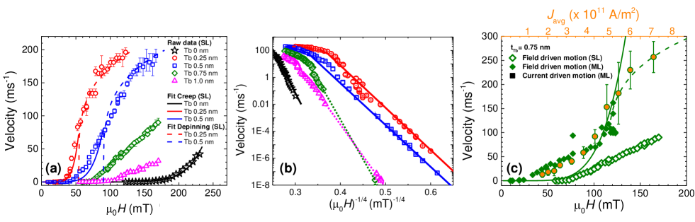
The impact of AFM coupling on the dynamical behavior of the DW has been investigated through two series of measurements where they are driven either by out-of-plane magnetic field or by current pulses. First we examine the field induced DW motion. The velocity curves for the different samples displayed in Fig.2 (a) and (b) for the SL samples with various reveal the pinning dependent regimes for the DW dynamics. For clarity, we will use consistent color schemes throughout the article to represent data for samples with different . It is important to note that for all the curves, we set the upper limit of the explored magnetic field range based on the field at which multiple domain nucleation events are observed during the magnetic field pulse, as this interferes with velocity measurements. For the same reason, measurements could also not be conducted for ML samples with nm. As observed, changing strongly alters the shape of velocity curves and the field range over which significant velocities are observed. Specifically, increasing shifts the curves towards larger magnetic fields except for the film without Tb, which is observed at the highest field. To identify the different dynamical regimes and quantitatively analyze the evolution of DW pinning with , the velocity curves have been compared to (i) the self-consistent description of the creep regime (dashed lines, )
| (4) |
where is the thermal activation energy, the effective pinning barrier, and (ii) the depinning regime in non-thermally activated limit (solid lines, ), given by
| (5) |
as developed for ferromagnetic ultrathin films [9, 10, 14]. In Eqs. 4 and 5, , and are the universal parameters of the quenched Edwards Wilkinson universality class for thin films and short range pinning interactions. The depinning field , temperature , and velocity are material dependent parameters reflecting the interaction of the DW with disorder. Eqs. 4- 5 describe the dynamics resulting from intricate and cooperative processes shaped by multiple influential factors, namely the interplay between the external driving field, DW elasticity, thermal fluctuations, and inherent disorder of the sample.
As observed in Fig. 2(a) and (b), the experimental velocities for the different samples fit rather well with the expectations (plain line) from the creep law (Eq. 4) in the lowest field drive range. Note that the curves for and nm present (red and blue in Fig. 2(a)) a change between positive and negative curvature compatible with a crossover between creep and depinning regimes. For nm, the negative curvature is not observed, indicating that the depinning regime has not been reached. As increases from to nm, we find that the fit with creep law just below the depinning field is not very good. The linear variation of the velocity observed for nm and nm is not typically seen for ferromagnetic films, suggesting that it may be characteristic of DW dynamics in AFM systems. A possible explanation could be a divergence of the avalanche sizes close to depinning. However, the absence of quantitative agreement with the prediction of Ref. [46] leaves the origin of this behavior as an open question which goes beyond the scope of this work. The depinning parameters (, , and ) reported in Table 1 for and nm were determined by the fits of Eqs. 4-5. For the other , we assume that the maximum measured velocity is the one close to the depinning transition: the maximum measured field and velocity correspond to and , respectively. The depinning temperature is then defined by the best fit of the creep regime (see the dotted lines in Fig. 2(b)).
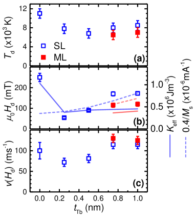
As shown in Fig. 3, the depinning field displays a non-monotonous variation. We find that presents a strong reduction (by a factor 5) between 0 and 0.25 nm of and then increases strongly (by more than a factor 3) between 0.25 and 1.0 nm. The strong reduction of between and 0.25 nm coincides with the sharp increase of the anisotropy. Then by assuming a constant pinning force, as the driving force is proportional to , the decrease of with increasing between 0.25 and 1.0 nm is expected to increase the depinning field . In Fig. 3(b), is traced as solid line to demonstrate how the anisotropy jump as the first Tb layer is inserted correlates with . After the initial jump corresponding to the insertion of Tb, correlates with as displayed by a dotted line.
For the ML samples, the values of are smaller than those for the SL samples. This is attributed to a reduction in anisotropy caused by the incremental increase in Co thickness and the influence of dipolar coupling within the ML structure. It also corresponds to the evolution of the BLS peaks linewiths. For , the variations are also non-monotonous: a pronounced decrease is observed in the SL samples when the first layer of Tb is inserted (from to nm). This confirms that the DW pinning is significantly reduced by the introduction of Tb layer in the system. Henceforth, the change in with further Tb insertion is less significant. The continuous increase observed is still correlated with the rise of . As the depinning velocity depends on and on the shape of the velocity curves, it is often misleading to comment on the trend of the velocity. Nevertheless, we observe an increase in with as well as from the SL to the ML samples. In summary, we find that (i) the strong reduction of the film anisotropy with nm coincides with a strong reduction of , (ii) the increase of reduces , due to AFM coupling between Co and Tb, which enhances , and (iii) the behaviors are quantitatively similar for SL and ML samples.
III.3 Current-induced DW dynamics
In Fig. 2 (c), we present the velocity curves obtained for magnetic field driven DW motion in SL (open diamond), in ML (plain diamond) and for current driven DW motion in ML (open circle filled with orange) with a fixed Tb thickness (=0.75 nm). As observed, the linear variation of the velocity in the low driving range found in SLs is also observed for the ML sample. The apparent shift of about mT is partly due to the larger in the ML sample. To compare between current and field driven DW motion, we used a single multiplicative conversion factor to rescale the current density (). We observe that the two curves are consistent with a crossover between creep and depinning, as indicated by their comparison with the predictions of Eqs. 4- 5. The overlap of the curves suggests an equivalence between SOT and a perpendicular magnetic field, as predicted for free DW motion [27] in the limit (which is justified here as one computes A/m2 for the ML with nm, assuming a damping constant ), and neglecting the FL torque (see App. C for justification).
To gain further insight into the contribution of AFM coupling on DW driven by SOT, the conversion factor () was estimated for all the samples studied. It is important to highlight that the field-driven DW motion experiments were performed on all SL and some ML samples, as detailed in the previous section. However, current-induced DW motion experiments were only conducted on the ML samples. Therefore, the SL series may provide another comparison between field-induced and current-induced DW motion. In appendix C (see Fig. 8), we show the conversion factor plotted as a function of where the current density is calculated as it was uniform through all the layers within the heterostructure and is the magnetic layers (Co+Tb) thickness that was used to calculate . A monotonous increase in the efficiency as a function of is found by virtue of the AFM coupling in both the SL and ML samples. The increasing trend of the conversion factor aligns well with the modified model, as explained by the Thiele force equation approach [27]:
| (6) |
where is the Planck constant, is the effective spin Hall angle, and for pure transversal Néel walls ( is the angle between the current density and the in-plane magnetization direction in the DW).
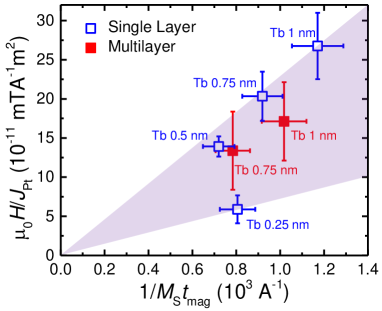
An accurate estimation of requires to disentangle the actual proportion of current flowing through different layers within the ML structure. Previous research has shown that the predominant source of SOT arises from the PtCo interface [43]. Therefore, the conversion factor has been calculated in terms of current flowing through the Pt layers () only. The current density through the individual layers has been estimated by measuring their resistivity in four-point geometries. The resistivity of Ta, Co, and Pt films of similar thicknesses are respectively 169, 30 and 24 cm. The current density through the Tb and Al layers has been neglected due to the high resistivity of these materials at the thicknesses that we experimentally measured. To estimate the current density in the Pt layers, we used [43]:
| (7) |
where is the total thickness of the heterostructure. In Fig. 4, we present the rescaled conversion factor () as a function of . The data in Fig. 4 can be fitted using Eq. 6, substituting by . The data points show some dispersion and do not strictly follow a linear trend. To account for this variability, we have shaded a region in Fig. 4 to represent the fitting range, capturing the dispersion of the individual points. Within this region, we estimate , attributing the primary sources of SOT to the PtCo interfaces. Additionally, the effective spin Hall angle was measured in the SL samples using the second harmonic Hall measurement technique (see Appendix D for details), in which the bottom 8 nm Pt is again considered being the only source of SOT. There are several potential reasons for the mismatched values obtained from the two different measurement methods. One reason is that the ML and SL samples used for current- and field-induced dynamic measurements were not identical, as previously noted. However, as shown in Fig.4, the SL points are in the same range of values as the ML points. Additionally, the Joule heating produced by the current pulse is expected to heat the track [47, 48]. For a typical current density A, and pulse duration ns, the heat is expected to be confined into the layer just below the track (see Appendix E for details). The estimated temperature rise K is rather large. On the one hand, it is expected to reduce significantly the DW width parameter and to produce highly non-linear velocity enhancement [48]. In addition, the associated decrease of the spontaneous magnetization directly increases (see Eq. 6) the effective field due to the SOT. Analyzing the contribution of Joule heating to DW velocity for each value of current density and accounting for the dynamical regimes (creep, depinning, and flow) followed by DW is beyond the scope of this work. On the other hand, another source of error arises from the calculation of , due to the intrinsic complexities and assumptions involved in this method. Taking these factors into account, we believe that the spin Hall angle estimated from the DW dynamic measurements is in reasonable agreement with the results from the second Harmonic Hall measurements. This alternative method for estimating the spin Hall angle in multilayers is interesting, as traditional techniques like second harmonic Hall or inverse spin Hall effect measurements, along with their analyses, can be cumbersome.
III.4 Influence of DW disorder interaction
To discuss the evolution of the interaction between DWs and disorder with the Tb thickness in SL and ML, we apply the scaling model developed in Ref. [49]. This model relates the depinning parameters ( and ) to the characteristic length scale and the force of the DW disorder interaction :
| (8) | |||
| (9) |
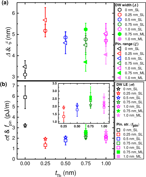
where the is the DW energy density with pJ/m the exchange stiffness, is the Boltzmann constant, and is a characteristic distance between pinning sites. From the data of table I, we obtain the variations of and as a function of shown in Fig. 5(a). We first compare the variation of DW width parameter and . For the DW width , we find a strong increase between 0 and 0.25nm of Tb, associated to the decrease of by the factor 3 (see Table I). The values obtained for the MLs remains close to those obtained for the SLs. As for the pinning range , we observe a good scaling for all . We used a single scaling factor (=1.5) for to obtain the best superimposition between with the values of . This result is compatible with a typical distance between pinning centers smaller than the DW thickness (), which thus corresponds to the DW pinning range [49, 50].
In Fig. 5(b), we compare the variation of the pinning strength and the DW line energy as a function of . For the DW energy , we find a strong decrease between and nm associated to the jump of . For the calculation of , we choose arbitrarily nm and use a single scaling factor () to obtain the best superposition with . Between and 1 nm, variations of scale rather well with those of , in agreement with the findings of Refs. [49, 50], which were obtained with a fixed disorder. Therefore, the good scaling strongly suggests that the elaboration method is sufficiently reliable to produce a reproducible pinning disorder. Note also that and present opposite curvature for their variations with . Such behavior is expected since for , the interaction of DW is smoothed over the DW thickness. For a fixed disorder, reducing is expected to enhance the interaction strength. Moreover, it should be noted that without Tb layer, a bad scaling between and is observed [Fig. 5(b)]. Therefore, the changes of effective anisotropy and magnetization with at the origin of the scaling between and are not sufficient to explain the variation of DW pinning. The high value of suggests that the pinning strength is larger for the CoAl interface than for the CoTb interface. This effect may be both associated to enhanced fluctuations of effective anisotropy and to a reduced correlation of pinning disorder.
IV Conclusion
In conclusion, we have investigated the impact of incorporating a Tb layer in PtCoAl synthetic ferrimagnetic multilayers on field- and current-driven DW motion. We show that inserting a Tb layer between the Co and Al layers reduces anisotropy, thereby weakening the interaction strength between the DW and disorder. This antiferromagnetic coupling leads to a decrease in pinning strength, resulting in faster DW motion. Additionally, we introduce a novel method to quantify effective spin torques in these multilayers by analyzing the depinning transitions. Our work not only enhances our understanding of DW mobility in ferrimagnetic multilayers but also offers strategies for optimizing spin-orbit torques and pinning landscapes. We believe this research is a crucial step towards the realization of DW logic and memory devices using antiferromagnetic or ferrimagnetic materials, bridging the gap between theoretical understanding and practical implementation.
Acknowledgements.
We acknowledge Dr. Yanis Sassi for sharing data of PtCoAl multilayers, Dr. Sachin Krishnia and Dr. Henri Jaffrès for fruitful discussion. The XMCD experiments were performed on the DEIMOS beamline at SOLEIL Synchrotron, France and the authors are grateful to the SOLEIL staff for smoothly running the facility. This work has been financially supported by a government grant managed by the French ANR as part of the “Investissements d’Avenir” program (Labex NanoSaclay, SPiCY ANR-10-LABX-0035) and as a part of the France 2030 investment plan from PEPR SPIN CHIREX ANR-22-EXSP-0002 and SPINMAT ANR-22-EXSP-0008. We also ackowledge the support from the Horizon2020 Framework Program of the European Commission, under FETProactive Grant agreement No. 824123 (SKYTOP) (H2020 FET proactive 824123).Appendix A XMCD data treatment
In Fig.6 (a) and (b), we show the raw XAS spectra acquired with an external out-of-plane magnetic field of 2 T with right-circular (CR: green) and left-circular (CL: pink) polarized light for Co and Tb, respectively. The displayed XAS spectra for each polarization are averages of several summed XAS measurements. The remaining XAS background is removed to determine by subtracting the linear interpolation of the off-peak intervals from the raw spectra for each polarization [37]. The data has been normalized at the pre-edge to coincide with 0, and further renormalized at the post-edge to 1. The normalized average XAS spectra () are shown in Fig.1 (a) and (b). The XMCD signal is obtained by subtracting the normalized CL spectra from the normalized CR spectra (for “positive” field). Note that the error in XMCD measurements predominantly arises during total electron yield, due to a distortion of the XAS from saturation effects [51]. For the error bars, we have used the difference in values obtained from various spectra in the same configuration or with reversed magnetic field.
Appendix B BLS Measurements
In order to estimate the interfacial DMI in the heterostructure, BLS measurements have been performed in Damon-Eschbach geometry on the ML samples with lower Tb thicknesses of and nm. It should be noted that the linewidth of the peaks was observed to increase markedly as Tb thickness increased as seen in Fig. 7. In addition, this linewidth was also seen to decrease when comparing ML to SL samples (data not shown here). The DMI can be extracted using . We find respectively and mJ m-2 for the SL and ML samples with nm and mJ m-2 for the ML sample with nm.
Appendix C Comparison of field- and current-induced motion
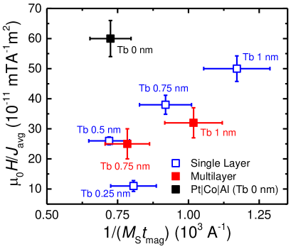
In Fig. 8, we show the conversion factor () plotted as a function of where the current density is calculated as if it was uniform through all the layers within the heterostructure. To ensure accurate selection of , the values have been extracted from XMCD and SQUID measurements for the SL and ML samples, respectively. A monotonous increase in the efficiency has been observed in all the samples. It is important to note that current-induced DW motion experiments have been conducted exclusively on ML samples, while field-induced DW motion experiments have been performed on both SL and ML samples. To compare the results from these two types of experiments, the conversion factor has been used as a scaling factor to superimpose the data. We note that the conversion factor is rather small for the SL sample with nm. This is primarily due to the strong drop in anisotropy with the insertion of Tb layer into the heterostructure. Additionally, the Tb layer thickness is less than a monolayer for this sample, leaving the system not well optimized for efficient SOT driven DW motion.
Appendix D Second harmonic Hall measurements
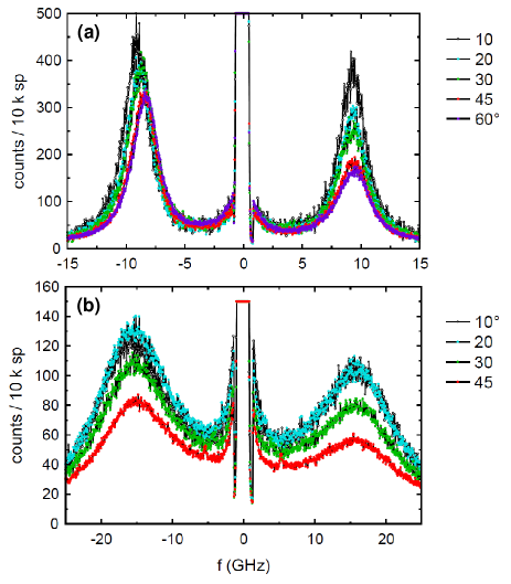
Harmonic Hall voltage measurement technique has been used to quantify the damping-like (DL) torque in the SL samples. For the DL geometry, the current has been applied in-plane parallel to the external field. The Hall voltage can be represented as [52, 53]:
| (10) | ||||
| (11) | ||||
| (14) |
where and are the polar and azimuth angles of magnetization, respectively, is the anomalous Hall resistance, is the planar Hall resistance, and is a spurious resistance due to imperfection in the device. The ordinary Hall resistance is negligible. When an ac current of angular frequency is injected into the Hall bars, it generates effective SOT fields that produce magnetic oscillations around equilibrium. These oscillations modulate the Hall voltage in synchronization with the current. Notably, provides information about the magnetization direction in the presence of an external magnetic field, whereas contains information about the magnetization oscillations generated by the torques. To extract the SOT effective field (), we simultaneously measure and as a function of the in-plane magnetic field. The external magnetic field is applied slightly off-plane at an angle rad ( degrees) to ensure uniform magnetization inside the Hall bar. In DL geometry (, ):
| (15) |
and, in field-like (FL) geometry (, ):
| (16) |
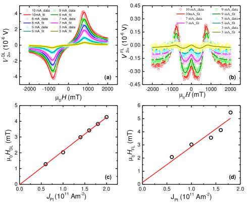
and are the DL and FL effective fields, respectively. , , and are extracted from . By fitting eqs. 15 and 16 simultaneously as a function of and , the and are extracted as a function of the . Additionally, we note that is one order of magnitude smaller than and hence that the fits are dominated by the first terms of eqs. 15 and 16. The fitting of in DL and FL geometry is shown in Fig. 9(a) and (b), respectively for the SL sample with 0.25 nm. Additionally, the variation of and as a function of is shown in Fig. 9(c), and (d), respectively. From the best fit of Fig. 9(b), we obtain mT A-1m2 and mT A-1m2. Subsequently, the spin Hall angle has been estimated by:
| (17) |
We note that while can be extracted independently from equations 6 and 17, their forms are not identical due to the field representing two different physical quantities. The field in Eq. 6 represents the precessional term in the LLG equation whereas the DL effective field corresponds to the damping term. We note that the FL effective field is of the same order of magnitude as the DL field, questioning its being neglected in the analysis. The reason is that this field does not drive the domain walls, but competes with the DMI and the Néel wall demagnetizing fields. As for a typical current density at depinning of A/m2 one has mT it is clear that neglecting it is justified in first approximation.
Appendix E Joule heating and current induced DW dynamics
A rough estimation of the temperature rise produced by Joule heating can be obtained by considering the heat diffusion through the layer below the track [47, 48]. Indeed, the heat diffusion length is given by , where is the heat diffusion coefficient, with the thermal conductivity, the specific hear and the density. For the values of (, , and ) and a typical current pulse duration , the diffusion length is smaller than layer thickness of 280 nm. Therefore, during the current pulse, the heat should propagate only just below the track without reaching significantly the Si substrate. The heated volume should be of the order of leading to a temperature rise , where is the power dissipated ( are the track width, thickness, and length, respectively). For the track resistance and typical current density A, the estimated temperature rise is . This large value essentially results from the very low heat conductivity of the layer (which is two orders of magnitude lower than for Si and GaAs).
References
- Kumar et al. [2022] D. Kumar, T. Jin, R. Sbiaa, M. Kläui, S. Bedanta, S. Fukami, D. Ravelosona, S.-H. Yang, X. Liu, and S. Piramanayagam, Domain wall memory: Physics, materials, and devices, Phys. Rep. 958, 1 (2022).
- Allwood et al. [2005] D. A. Allwood, G. Xiong, C. C. Faulkner, D. Atkinson, D. Petit, and R. P. Cowburn, Magnetic domain-wall logic, Science 309, 1688 (2005).
- Parkin et al. [2008] S. S. P. Parkin, M. Hayashi, and L. Thomas, Magnetic domain-wall racetrack memory, Science 320, 190 (2008).
- K. Behera et al. [2020] A. K. Behera, C. Murapaka, S. Mallick, B. B. Singh, and S. Bedanta, Skyrmion racetrack memory with an antidot, J. Phys. D: Appl. Phys. 54, 025001 (2020).
- Kim et al. [2017] K.-J. Kim, S. K. Kim, Y. Hirata, S.-H. Oh, T. Tono, D.-H. Kim, T. Okuno, W. S. Ham, S. Kim, G. Go, Y. Tserkovnyak, A. Tsukamoto, T. Moriyama, K.-J. Lee, and T. Ono, Fast domain wall motion in the vicinity of the angular momentum compensation temperature of ferrimagnets, Nat. Mater. 16, 1187 (2017).
- Miron et al. [2011] I. M. Miron, T. Moore, H. Szambolics, L. D. Buda-Prejbeanu, S. Auffret, B. Rodmacq, S. Pizzini, J. Vogel, M. Bonfim, A. Schuhl, and G. Gaudin, Fast current-induced domain-wall motion controlled by the rashba effect, Nat. Mater. 10, 419 (2011).
- Mallick et al. [2018] S. Mallick, S. S. Mishra, and S. Bedanta, Relaxation dynamics in magnetic antidot lattice arrays of co/pt with perpendicular anisotropy, Scientific Reports 8, 11648 (2018).
- Gorchon et al. [2014] J. Gorchon, S. Bustingorry, J. Ferré, V. Jeudy, A. B. Kolton, and T. Giamarchi, Pinning-dependent field-driven domain wall dynamics and thermal scaling in an ultrathin magnetic film, Phys. Rev. Lett. 113, 027205 (2014).
- Jeudy et al. [2016] V. Jeudy, A. Mougin, S. Bustingorry, W. Savero Torres, J. Gorchon, A. B. Kolton, A. Lemaître, and J.-P. Jamet, Universal pinning energy barrier for driven domain walls in thin ferromagnetic films, Phys. Rev. Lett. 117, 057201 (2016).
- Jeudy et al. [2018] V. Jeudy, R. Díaz Pardo, W. Savero Torres, S. Bustingorry, and A. B. Kolton, Pinning of domain walls in thin ferromagnetic films, Phys. Rev. B 98, 054406 (2018).
- Ojha et al. [2023a] B. Ojha, S. Mallick, S. Panigrahy, M. Sharma, A. Thiaville, S. Rohart, and S. Bedanta, Driving skyrmions with low threshold current density in pt/cofeb thin film, Physica Scripta 98, 035819 (2023a).
- Ojha et al. [2023b] B. Ojha, B. B. Singh, M. Sharma, S. Mallick, V. Jeudy, A. Thiaville, S. Rohart, and S. Bedanta, Unusual domain wall motion in the vicinity of the depinning field in a pt/cofeb/mgo film, Appl. Phys. A 129, 688 (2023b).
- Kim et al. [2009] K.-J. Kim, J.-C. Lee, S.-M. Ahn, K.-S. Lee, C.-W. Lee, Y. J. Cho, S. Seo, K.-H. Shin, S.-B. Choe, and H.-W. Lee, Interdimensional universality of dynamic interfaces, Nature 458, 740 (2009).
- Diaz Pardo et al. [2017] R. Diaz Pardo, W. Savero Torres, A. B. Kolton, S. Bustingorry, and V. Jeudy, Universal depinning transition of domain walls in ultrathin ferromagnets, Phys. Rev. B 95, 184434 (2017).
- Siddiqui et al. [2018] S. A. Siddiqui, J. Han, J. T. Finley, C. A. Ross, and L. Liu, Current-induced domain wall motion in a compensated ferrimagnet, Phys. Rev. Lett. 121, 057701 (2018).
- Gomonay et al. [2016] O. Gomonay, T. Jungwirth, and J. Sinova, High antiferromagnetic domain wall velocity induced by néel spin-orbit torques, Phys. Rev. Lett. 117, 017202 (2016).
- Panigrahy et al. [2022] S. Panigrahy, S. Mallick, J. Sampaio, and S. Rohart, Skyrmion inertia in synthetic antiferromagnets, Phys. Rev. B 106, 144405 (2022).
- Kleemann [2007] W. Kleemann, Universal domain wall dynamics in disordered ferroic materials, Ann. Rev. Mater. Res. 37, 415 (2007).
- Ferré et al. [2013] J. Ferré, P. J. Metaxas, A. Mougin, J.-P. Jamet, J. Gorchon, and V. Jeudy, Universal magnetic domain wall dynamics in the presence of weak disorder, Comp. Rend. Phys. 14, 651 (2013).
- Chowdhury et al. [2016] N. Chowdhury, S. Mallick, S. Mallik, and S. Bedanta, Study of magnetization relaxation in co thin films prepared by substrate rotation, Thin Solid Films 616, 328 (2016).
- Song et al. [2018] C. Song, Y. You, X. Chen, X. Zhou, Y. Wang, and F. Pan, How to manipulate magnetic states of antiferromagnets, Nanotechnology 29, 112001 (2018).
- Mallick et al. [2024a] S. Mallick, P. Ye, W. Boutu, D. Gauthier, H. Merdji, M. Bibes, M. Viret, K. Bouzehouane, and V. Cros, Oam driven nucleation of sub-50 nm compact antiferromagnetic skyrmions, Adv. Funct. Mater. 34, 2409528 (2024a).
- Stanciu et al. [2006] C. D. Stanciu, A. V. Kimel, F. Hansteen, A. Tsukamoto, A. Itoh, A. Kirilyuk, and T. Rasing, Ultrafast spin dynamics across compensation points in ferrimagnetic : The role of angular momentum compensation, Phys. Rev. B 73, 220402 (2006).
- Haltz et al. [2021] E. Haltz, S. Krishnia, L. Berges, A. Mougin, and J. a. Sampaio, Domain wall dynamics in antiferromagnetically coupled double-lattice systems, Phys. Rev. B 103, 014444 (2021).
- Berges et al. [2022] L. Berges, E. Haltz, S. Panigrahy, S. Mallick, R. Weil, S. Rohart, A. Mougin, and J. a. Sampaio, Size-dependent mobility of skyrmions beyond pinning in ferrimagnetic gdco thin films, Phys. Rev. B 106, 144408 (2022).
- Chanthbouala et al. [2011] A. Chanthbouala, R. Matsumoto, J. Grollier, V. Cros, A. Anane, A. Fert, A. V. Khvalkovskiy, K. A. Zvezdin, Y. N. K. Nishimura, H. Maehara, K. Tsunekawa, A. Fukushima, and S. Yuasa, Vertical-current-induced domain-wall motion in mgo-based magnetic tunnel junctions with low current densities, Nat. Phys. 7, 626 (2011).
- Thiaville et al. [2012] A. Thiaville, S. Rohart, Émilie Jué, V. Cros, and A. Fert, Dynamics of dzyaloshinskii domain walls in ultrathin magnetic films, Europhys. Lett. 100, 57002 (2012).
- Emori et al. [2013] S. Emori, U. Bauer, S.-M. Ahn, E. Martinez, and G. S. D. Beach, Current-driven dynamics of chiral ferromagnetic domain walls, Nat. Mater. 12, 611 (2013).
- Mallick et al. [2022] S. Mallick, S. Panigrahy, G. Pradhan, and S. Rohart, Current-induced nucleation and motion of skyrmions in zero magnetic field, Phys. Rev. Appl. 18, 064072 (2022).
- Mallick et al. [2024b] S. Mallick, Y. Sassi, N. F. Prestes, S. Krishnia, F. Gallego, L. M. V. Arche, T. Denneulin, S. Collin, K. Bouzehouane, A. Thiaville, R. E. Dunin-Borkowski, V. Jeudy, A. Fert, N. Reyren, and V. Cros, Driving skyrmions in flow regime in synthetic ferrimagnets, Nat. Commun. 15, 8472 (2024b).
- Ohresser et al. [2014] P. Ohresser, E. Otero, F. Choueikani, K. Chen, S. Stanescu, F. Deschamps, T. Moreno, F. Polack, B. Lagarde, J.-P. Daguerre, F. Marteau, F. Scheurer, L. Joly, J.-P. Kappler, B. Muller, O. Bunau, and P. Sainctavit, DEIMOS: A beamline dedicated to dichroism measurements in the 350–2500 eV energy range, Rev. Sci. Ins. 85, 013106 (2014).
- Belmeguenai et al. [2015] M. Belmeguenai, J.-P. Adam, Y. Roussigné, S. Eimer, T. Devolder, J.-V. Kim, S. M. Cherif, A. Stashkevich, and A. Thiaville, Interfacial dzyaloshinskii-moriya interaction in perpendicularly magnetized pt/co/al ultrathin films measured by brillouin light spectroscopy, Phys. Rev. B 91, 180405 (2015).
- Jué et al. [2016] E. Jué, A. Thiaville, S. Pizzini, J. Miltat, J. Sampaio, L. D. Buda-Prejbeanu, S. Rohart, J. Vogel, M. Bonfim, O. Boulle, S. Auffret, I. M. Miron, and G. Gaudin, Domain wall dynamics in ultrathin pt/co/al microstrips under large combined magnetic fields, Phys. Rev. B 93, 014403 (2016).
- Singha et al. [2017] A. Singha, R. Baltic, F. Donati, C. Wäckerlin, J. Dreiser, L. Persichetti, S. Stepanow, P. Gambardella, S. Rusponi, and H. Brune, occupancy and magnetism of rare-earth atoms adsorbed on metal substrates, Phys. Rev. B 96, 224418 (2017).
- Chen et al. [1995] C. T. Chen, Y. U. Idzerda, H.-J. Lin, N. V. Smith, G. Meigs, E. Chaban, G. H. Ho, E. Pellegrin, and F. Sette, Experimental confirmation of the x-ray magnetic circular dichroism sum rules for iron and cobalt, Phys. Rev. Lett. 75, 152 (1995).
- Suzuki et al. [2023] D. H. Suzuki, M. Valvidares, P. Gargiani, M. Huang, A. E. Kossak, and G. S. D. Beach, Thickness and composition effects on atomic moments and magnetic compensation point in rare-earth transition-metal thin films, Phys. Rev. B 107, 134430 (2023).
- Schillé et al. [1993] J. P. Schillé, J. P. Kappler, P. Sainctavit, C. Cartier dit Moulin, C. Brouder, and G. Krill, Experimental and calculated magnetic dichroism in the ho 3d x-ray-absorption spectra of intermetallic , Phys. Rev. B 48, 9491 (1993).
- Streubel et al. [2018] R. Streubel, C.-H. Lambert, N. Kent, P. Ercius, A. T. N’Diaye, C. Ophus, S. Salahuddin, and P. Fischer, Experimental evidence of chiral ferrimagnetism in amorphous gdco films, Adv. Mater. 30, 1800199 (2018).
- Teramura et al. [1996] Y. Teramura, A. Tanaka, B. Thole, and T. Jo, Effect of coulomb interaction on the x-ray magnetic circular dichroism spin sum rule in rare earths, J. Phys. Soc. Japan 65, 3056 (1996).
- Jaccarino and Walker [1965] V. Jaccarino and L. R. Walker, Discontinuous occurrence of localized moments in metals, Phys. Rev. Lett. 15, 258 (1965).
- Buschow et al. [1977] K. Buschow, M. Brouha, J. Biesterbos, and A. Dirks, Crystalline and amorphous rare-earth transition metal alloys, Physica B+C 91, 261 (1977).
- Hansen et al. [1989] P. Hansen, C. Clausen, G. Much, M. Rosenkranz, and K. Witter, Magnetic and magneto‐optical properties of rare‐earth transition‐metal alloys containing Gd, Tb, Fe, Co, J Appl. Phys. 66, 756 (1989).
- Krishnia et al. [2023] S. Krishnia, Y. Sassi, F. Ajejas, N. Sebe, N. Reyren, S. Collin, T. Denneulin, A. Kovács, R. E. Dunin-Borkowski, A. Fert, J.-M. George, V. Cros, and H. Jaffrès, Large interfacial rashba interaction generating strong spin–orbit torques in atomically thin metallic heterostructures, Nano Lett. 23, 6785 (2023).
- Nistor et al. [2011] C. Nistor, T. Balashov, J. J. Kavich, A. Lodi Rizzini, B. Ballesteros, G. Gaudin, S. Auffret, B. Rodmacq, S. Dhesi, and P. Gambardella, Orbital moment anisotropy of pt/co/al heterostructures with strong rashba interaction, Phys. Rev. B 84, 054464 (2011).
- Krishnia et al. [2024] S. Krishnia, L. Vojáček, T. D. C. S. C. Gomes, N. Sebe, F. Ibrahim, and et al., Tuning interfacial orbital and spin related effects at CoAl interface with different oxidation level (2024), submitted to Phys. Rev. Lett.
- Caballero et al. [2018] N. B. Caballero, E. E. Ferrero, A. B. Kolton, J. Curiale, V. Jeudy, and S. Bustingorry, Magnetic domain wall creep and depinning: A scalar field model approach, Phys. Rev. E 97, 062122 (2018).
- Curiale et al. [2010] J. Curiale, A. Lemaître, G. Faini, and V. Jeudy, Track heating study for current-induced domain wall motion experiments, Appl. Phys. Lett. 97, 243505 (2010).
- Curiale et al. [2012] J. Curiale, A. Lemaître, T. Niazi, G. Faini, and V. Jeudy, Joule heating and current-induced domain wall motion, J. Appl. Phys. 112, 103922 (2012).
- Géhanne et al. [2020] P. Géhanne, S. Rohart, A. Thiaville, and V. Jeudy, Strength and length scale of the interaction between domain walls and pinning disorder in thin ferromagnetic films, Phys. Rev. Res. 2, 043134 (2020).
- Balan et al. [2023] C. Balan, J. W. van der Jagt, J. Peña Garcia, J. Vogel, L. Ranno, M. Bonfim, D. Ravelosona, S. Pizzini, and V. Jeudy, Control of the interaction between pinning disorder and domain walls in Pt/Co/Al ultrathin films by He+ ion irradiation, Appl. Phys. Lett. 122, 162401 (2023).
- Nakajima et al. [1999] R. Nakajima, J. Stöhr, and Y. U. Idzerda, Electron-yield saturation effects in l-edge x-ray magnetic circular dichroism spectra of fe, co, and ni, Phys. Rev. B 59, 6421 (1999).
- Hayashi et al. [2014] M. Hayashi, J. Kim, M. Yamanouchi, and H. Ohno, Quantitative characterization of the spin-orbit torque using harmonic hall voltage measurements, Phys. Rev. B 89, 144425 (2014).
- Wu et al. [2019] H. Wu, Y. Xu, P. Deng, Q. Pan, S. A. Razavi, K. Wong, L. Huang, B. Dai, Q. Shao, G. Yu, X. Han, J.-C. Rojas-Sánchez, S. Mangin, and K. L. Wang, Spin-orbit torque switching of a nearly compensated ferrimagnet by topological surface states, Adv. Mater. 31, 1901681 (2019).