]These authors contributed equally.
]These authors contributed equally.
Visible-range excitons and electronic structure in double perovskite oxides
Abstract
Presence of excitons significantly influence the optoelectronic properties and potential applications of materials. Using combined theoretical and experimental tools, we investigate the absorption spectra of double perovskite oxides Ba2YO6 ( = Nb, Ta, Sb), Ba2ScO6 ( = Ta, Sb) and ScSbO6 (=Ca, Sr, Ba), allowing for a systematic variation of composition. We not only show that low-energy excitons are present in the visible range in all the considered so-called wide-gap insulators, but also that the nature and properties of these exciton modes differ from those in double perovskite halides as well as perovskite oxides. We provide insights on the origin of such differences by a detailed and comparative analysis of the electronic structure. Further, our findings elucidate possible correlations between the exciton properties and the composition, via the electronic structure, towards a comprehensive understanding of correlation effects and rational design principles.
I Introduction
Wide-gap insulators are considered promising for a variety of optoelectronic and photocatalytic applications [1, 2, 3, 4, 5, 6]. In general, varying degree of sensitivity to crystal structure and composition is found, and viability for specific applications is dictated by the electronic and optical properties [1, 3, 4, 5, 6]. The large-gap double perovskite oxides (DPOs), general formula , formed by transition metals with unfilled/empty valence -shells at the /-sites are considered promising in microwave-dielectric resonator applications, including interference filters, reflective coating and in optical fibers, due to their good dielectric properties, and as buffer materials due to their low reactivity [1, 3, 4]. Within this materials class, a wide range of optoelectronic properties can be tuned by suitable modulation of composition [2]. For example, a bandgap increase of up to 2 eV can be realized with increasing octahedral tilting and distortions [1, 3]
Further, many body effects, such as the presence of bound electron-hole pair quasiparticles — the so-called excitons, can lead to sub-gap features in optical properties. An accurate knowledge of electronic and optical properties, including the details of exciton modes, is thus important. The exciton binding energy is also useful to determine charge recombination, an important parameter for devices. In addition, these excitons may find applications in excitonic emission [7], photocatalysis [8], energy devices [9, 10] and even information processing [11]. As a result, there is a growing interest in the study of excitons in a variety of materials due to potential optoelectronic applications [12, 13]. However, systematic studies on detailed characterization of excitons and possible correlations between the electronic properties and the exciton properties are limited.
An exciton is an electron-hole pair bound together by Coulomb interaction. Formation of excitons in semiconductors and insulators is well-known [14, 15, 16, 17, 18, 19, 20] and occurs upon irradiation by light. Due to their binding energy, their presence is often detected by peaks in the electronically forbidden energy range (bandgap) in the absorption spectrum [21, 22, 23, 24, 25], and the photoluminiscence spectra [26, 7]. Predictions for real materials require density functional (DF) calculations incorporating many body effects [27] via the Bethe-Salpeter equation (BSE) [28, 29] which, unfortunately, is computationally quite demanding. Therefore, reliable predictions for real materials are scarce.
In the double perovskite halides, based on solution to BSE, it is predicted that both hydrogenic (Wannier-Mott) and non-hydrogenic excitons are present, and that the binding energies can be as large as 2 eV [12]. The nature and the properties of the exciton modes is composition dependent, e.g. presence of indirect bandgaps and large effective electron/hole mass anisotropies stabilize non-hydrogenic excitons which are highly delocalized in the reciprocal space.
On the other hand, in certain transition metal oxides with partially occupied valence -states, the excitons are spatially localized within a radius of the order of metal-oxygen bonds [30]. In non-magnetic perovskite oxides with configuration, the contributions from the band edge states with dominant -character, depend on the composition and can lead to large exciton binding energies up to 6 eV [31]. For example, in SrTiO3 and KTaO3, the excitons are spatially delocalized with low-energy transitions to metal states, whereas in SrHfO3 and SrZrO3, transitions to states also contribute at low energies while the excitons are spatially localized. In both cases, the dominant contribution corresponds to transitions at the the -point. Deviation from cubic structures leads to sizable contributions from different -points as well, leading to spatially localized excitons.
For DPOs, therefore, a number of questions arise: How do the findings in perovskite oxides extend to double perovskites when two different transition metals are present? Especially, what happens if both the transition metals contribute at the conduction band (CB) edge? What if the conduction band edge does not have dominant contributions from the metal states but an extended -state instead? What is the role of ligand anions? Is it possible to extract reliable information about the excitons from the elementary electronic structure based on density functional theory (DFT) alone?
To address these concerns, here, we focus on -DPOs — a versatile playground to explore the effects of bandgap, crystal structure and composition [2]. Typically, divalent alkaline earth cations occupy the -sites, while the and sites are occupied by transition metal cations with effectively filled or empty -states, leading to an insulating state in O6 [1, 2, 3].
In particular, we consider the Sc and Y based DPOs, ScSbO6 (=Ba, Sr, Ca), Ba2YO6 ( = Ta, Nb, Sb) and Ba2ScO6 ( = Ta, Sb), and carry out a systematic and comparative analysis of the absorption spectra aided with DF calculations using the generalized gradient approximation (GGA) [32] and modified Becke-Johnson (mBJ) potentials [33, 34, 35]. The observed absorption spectra are analyzed using the Kubelka-Munk (KM) function (without excitons), Elliot formula for isolated exciton peaks and excitons at the band edge, and the underlying electronic structure (DFT).
We observe multiple low-energy peaks in the absorption spectra identified as exciton peaks. The peaks are of considerably weak intensity and extend all the way to the visible range, much below the corresponding bandgaps. Based on a high-quality fit of the low-energy part of the data, we obtain the binding energies and linewidths (FWHM) from these peaks. Effects of the crystal structure and composition, in terms of the electronic structure, on the origin and nature of these excitons is reported. Systematic variations in the peak shapes is found as the atoms/orbital contributions at the band edges. These findings elucidate the role of -site and -site cations on the sub-gap excitons in the low-energy optical spectra of the considered DPOs.
II Results and Discussions
II.1 Crystal Structures & Electronic Properties
Structurally ordered DPOs, O6, consist of transition metals and surrounded by an octahedra whose vertices are occupied by oxygen atoms forming O bonds. Therefore, ordered systems comprise of alternating corner sharing O6 and O6 octahedra stacked in all directions. The A-site ions occupy the interstitial voids created by these octahedra. Flexibility in the choice of these ions provide a large room to obtain suitable combinations for desired properties. For = Sc3+, Y3+ (trivalent cations) and = Nb5+, Sb5+, Ta5+ (pentavalent cations) with either unfilled () or fully-filled () valence -orbitals are nonmagnetic with large predicted electronic bandgaps [1, 36, 3, 37, 38].
The combination = Ba, Sr, Ca; = Sc, Y; = Nb, Ta, Sb, considered herein, offers a rich platform to systematically explore the role of -, -site cations. Their electronic and optical properties have been studied [1, 36, 3, 37, 38] and those are largely governed by their /-O bond lengths, angle, and covalency factors such as the hybridization, covalent/ionic radii and electronegativity in a complex way.
The considered compounds belong to two crystal structure types [39, 36, 3, 37, 38]: Due to large A-site cation, Ba-based compounds, viz. BSS, BST, BYT, and BYN crystallize in the face centered cubic structure, featuring linear -O- bonds (). With decreasing size of the -site cation, such as in SSS and CSS, tilting of the O6 and O6 octahedra leads to monoclinic structures with and , respectively, and [3, 39]. Table SI in Supplemental Information (SI) [40] lists the crystal structure details determined from the XRD data at room temperatures. The obtained and predicted structures agree with the often-used Goldschmidt tolerance factor [41] and are also mostly consistent with the recently introduced Bartel’s tolerance factor [42] (see SI for details).
The optical gaps obtained from the effective absorption spectra (Kubelka-Munk spectra; see Methods) obtained from the UV-Vis diffuse reflectance spectroscopy data is shown in Fig. 1. Evidently, all the compounds have gaps eV, consistent with previous studies [1, 3, 38], and thus belong to the wide-gap insulators class. Concurrently, all the synthesized compounds were off-white in color albeit with differing RGB compositions (different shades). This discrepancy suggests possible presence of exciton modes in the visible range. Indeed, the log-scale plots in sub-gap region suggests presence of multiple well-defined peaks in the absorption spectra, as discussed later.
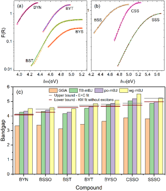
DF calculations, using the all-electron full-potential linear augmented plane waves (FP-LAPW) as implemented in the WIEN2k code [43, 44], find the ground state to be nonmagnetic and insulating for all the considered compounds as expected. Within GGA, a well-defined bandgap eV is found in all cases, as shown in Fig. 1(c), matching with previously reported values [1, 3, 38]. Changing the -site cation leads to enhancement of bandgaps, from BYN BYT BYS as well as BST BSS, while changing the -site cation from Y () to Sc () leads to lowering of bandgaps. At the same time, changing the -site cation also increases the bandgaps with smaller ion size. Importantly, the nature of bandgap is direct (at ) in BYN, BYT, BYS, BST and SSS, and indirect in BSS and CSS (). Even though, the trend in bandgap is consistent with the gaps found using the KM function (see Methods in SI and Fig 1 for details), these values are severely underestimated — a well-known issue with standard DFT [45, 46].
In order to address the issue of bandgap underestimation in DFT, we employ the efficient as well as accurate modified Becke-Johnson (mBJ) potentials [47, 48, 49, 50, 51]. Several flavors of the mBJ potentials are now available [33, 34, 35] suitable for perovskite oxides (’po-mBJ’) and wide-gap materials (’wg-mBJ’). All the considered mBJ-potentials show significant improvement over the GGA bandgap values (see Fig. 1(c)) while maintaining the nature of the bandgaps. Notably, the choice of DFT parameters, such as influences the electronic and optical properties only quantitatively. For brevity, we will consider the po-mBJ for further analysis.
The total and atom/orbital-resolved (partial) densities of states are shown in Fig. 2. Consistent with the formal valencies, as well as previous reports, the valence band edge is dominantly of O- character from the non-bonding oxygen states with negligible traces of other atoms/orbitals. In the presence of (and ) octahedra, the valence states of the transition metals undergo octahedral crystal field splitting, leading to the lower-lying and the states. The conduction band edge for compounds not containing Sb is, therefore, dominated by metal - states from either or site or both, which have three-fold degeneracy at not accounting for spin. Presence of Sb5+ ions, on the other hand, leads to a state with dominant character at the CB edge. The -site metal - states lie next (to the Sb- state) in the conduction band. Therefore, the low-energy electronic and optical properties are governed by these states near the Fermi energy.
Specifically, the direct gaps in BYN and BYT involve triplet states with dominant Nb- or Ta- characters, 3-fold degenerate at , at the CB edge. Small contributions from Y- states at the CB edge, for BYN and for BYT is also noted. In comparison, the larger but indirect gap in BYS is between the O- dominated states in valence band (VB) and the non-degenerate Sb- state at the CB edge, from (see Fig. 2(d)). At the same time, the relative Y- contribution at the CB edge is much larger.
Presence of Sc at the -sites leads to a significantly larger contribution () by the Sc - orbitals along with Ta - orbitals due to smaller radial extent of the valence Sc- states compared to Y- states, leading to large overlap with the O- states [1]. In BSS, the relative gap between the Sb- and Sc states is much smaller than in BST while the Sc contribution at the CB edge is comparable to that of Sb; nevertheless the CB edge is formed by the Sb- states.
On the other hand, changing the -site cation leads to symmetry lowering of the crystal structure, resulting in a significant change in the bandgaps even if their contributions at the band edge is tiny. The bandgap increases by 0.6 and eV, respectively for SSS and CSS [1, 3]. However, as shown in Fig. 2, in all the Sb based systems, Sb- states contribute dominantly at the CB edge. Deviation from cubic structure enhances the gap, but only quantitatively influences the electronic and optical properties [3].
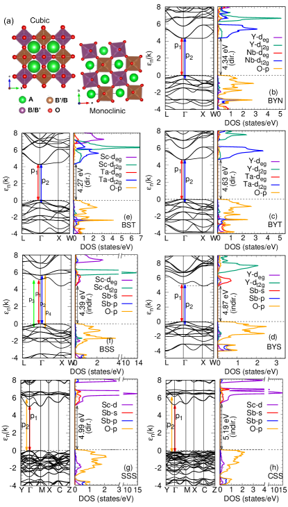
Essentially, all the synthesized compounds are oxygen to transition metal charge transfer complexes with large electronic bandgaps. In all cases, the VB edge is formed by the O- states whereas an isolated set of bands for the CB edge. Details of the CB edge depends on the composition: Variations in /-site ions can lead not only to transition from direct to indirect gaps, but also change the nature of the CB edge states (transition metal states vs Sb- states). At the same time, quantitative differences in terms of atom/orbital contributions exist. Of particular relevance are the dispersionless bands along at the band edges as well as presence of linear dispersions in non-Sb compounds. As they directly influence the effective mass of the electrons and holes, and the optical transition matrix elements [52], these features may have interesting consequence for the excitons in these systems.
II.2 Exciton modes & Optical properties
We now turn our attention to the primary focus of this study — presence of excitons and their possible correlation(s) with the electronic structure. In principle, as in double perovskites halides, both hydrogenic (Wannier-Mott) and non-hydrogenic excitons could be present [12]. Moreover, the present excitons modes may display a wide range of localization behavior as in transition metal oxides and perovskite oxides [19, 30, 31].
To identify the excitons modes, we analyze the observed low-energy absorption data and fit the low-energy peaks using the Elliot formula [25, 53], as discussed in detail in Ref. [38] (also see Methods). Although the Elliot formula used here relies on hydrogenic model of excitons, the procedure utilized here merely identifies the exciton peaks and the corresponding exciton binding energies and the electronic gap (presumed optical gap without excitons) of the materials. The hydrogenic model suggests that the exciton peaks scale as , where is the effective mass and is the static dielectric constant. In order to characterize the nature of excitons as non-hydrogenic, in principle, detailed knowledge of dielectric screening is thus required which is, however, not available for the considered compounds at present. Nevertheless, deviations from hydrogenic model are discussed based on the comparative analysis of the peak positions and their shapes. It is important to note that, since the absorption data for an indirect bandgap in presence of excitons mimic that of a direct bandgap system, the Kubelka Munk function is obtained assuming all materials to possess direct bandgap.
Fig. 3 shows the low-energy absorption spectra and the multiple-peak fit to the data. The details of the fit quality is provide in Table SII [40]. Evidently, in all the compounds considered, low-energy peaks are present well below the electronic gaps. Remarkably, these peaks extend well within the visible range of the electromagnetic spectrum (1.65 eV - 3.25 eV). The corresponding binding energies are found to lie between 2 eV to 3 eV. However, the peak intensities are quite small, leading to weak absorption in the visible range. This explains the origin of off-white colors of the considered compounds.
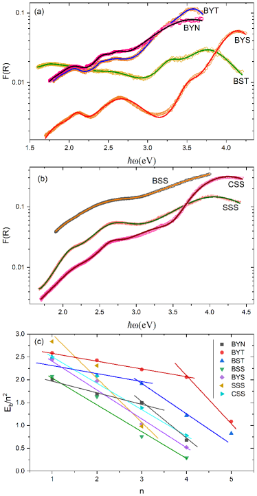
For cubic compounds not involving Sb (BYN, BYT, and BST), i.e. for compounds with - states at CB edge, one expects them to be well-described by the hydrogenic model as the systems are not only isotropic due to the cubic symmetry, but also possess direct bandgaps [12]. Additionally, the exciton characteristics is likely to be governed by the joint density of states (JDOS) for transitions from O- states to - states, as in perovskite oxides [31]. The obtained vs. in Fig 3(c), however, shows a weak deviation from the ideal behavior for small . Interestingly, large deviation is obtained for large , suggesting different possible origins of these peaks.
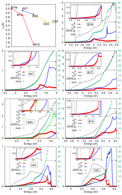
In comparison, the Sb compounds show significantly large deviations for all values of presumably due to presence of indirect bandgaps leading to non-hydrogenic excitons in all cases. (In Ca, the energy at the VB edge at is meV below the Fermi energy, .) The binding energies are smaller than others. Smaller binding energies arise due to weaker Coulomb interaction between the electrons and holes forming the excitons. Contradictory to that, the screening in Sb-compounds is much weaker as evidenced by their static dielectric constant values, albeit without many body effects, as shown in Fig. 4(a). Therefore, it seems that the large radial extent of the involved state compete with the screening effect, eventually leading to weak interaction between the electron-hole pair.
Role of indirect bandgaps in the nature of excitons in Sb-compounds is further attested by the fact that linewidths of the peaks are much larger than in others (see Table I and SI [40]) to the extent that low-energy absorption spectrum in BSS is rather featureless. At the same time, the absorption in ScSb-compounds is also higher. To gain further insights, we study the band-resolved imaginary part of the dielectric response , involving band sets and across . The 3-fold degenerate bands () at the CB edge and the sets of O--dominated bands degenerate at , and/or contribute at low-energies, being the number of electrons in the system. Sum over bands lead to and , respectively, which contribute at low energies.
Figure 4 shows the low-energy contributions to the dielectric function and the related JDOS. In all cases, vanishing optical-transition matrix elements despite large JDOS lead to sizable response away from the bandgap energies, implying no contribution at the -point, contrary to perovskite oxides [31]. Nevertheless, eV bandwidths of the dominant peaks in the band-resolved dielectric function (see SI for details) suggests rather finite extend of the identified excitons involving these edge states. Furthermore, the relatively smaller contribution of the edge transitions () compared to other contributions such as the sub-edge transitions may explain the weak intensity peaks in the absorption data. In fact, in some cases, the -contribution even starts at lower energies as shown in the insets of Fig. 4.
BYN and BYT display large edge contributions arising from optical transitions between the sub-edge O- below and the states forming the contribution. At the same time, changing the site, from Nb to Ta, results in no contribution at the (response) onset. The band-resolved contributions [40] further suggests no contrib from the dispersionless (flat) band along in both cases. In fact, in BYN, dominant contribution to arises close to the - and points whereas the gradual rise is likely due to contributions along . In comparison, -points along - contribute to the onset in BYT through . It is interesting to note the relative contribution of Y-- states at the CB edge is also slightly larger in BYN due to larger radial extent of states in Ta.
Presence of Sc at the -site, in BST, despite significant Sc contribution at the band edge (Fig. 2), also leads to the response onset due to contributions only. While the band-resolved contributions (see SI) is similar to BYT. contributions, however, show a dominant peak at low energies 5.5 eV, distinct from both BYT and BYN. In terms of the linewidths (FWHM), the lowest energy peak in these three compounds suggests similar radial extent as well as lifetimes of the excitons, likely of similar origin. Other peak characteristics are also remarkably similar between BYN and BST. The details of the peak fit and their characteristics are presented in Table SII [40].
| Comp. | (eV) | (eV) | (eV) | Dominant contrib. |
|---|---|---|---|---|
| BYN | 4.08 (dir.) | 2.01 | 0.14 | , |
| BYT | 4.66 (dir.) | 2.59 | 0.07 | |
| BYS | 4.67 (indir.) | 2.44 | 0.08 | |
| BST | 4.66 (dir.) | 2.59 | 0.07 | , |
| BSS | 4.28 (indir.) | 2.08 | 0.34 | |
| SSS | 4.98 (dir.) | 2.84 | 0.12 | , |
| CSS | 4.74 (indir.) | 2.50 | 0.20 |
In sharp contrast, the singular contribution at the CB edge in Sb-compounds with cubic symmetry leads to rather sharp response onset characterized by contribution as compared to the non-Sb cubic compounds. Detailed analysis of the band-resolved contributions suggests non-vanishing contribution from the -point unlike the non-Sb counterparts along with sizable contributions at the -point. Remarkably, the well separated Sb state at the CB edge leads to comparable and contributions, unlike in BSS where, despite the ”hybridization” of the Sc-- states with the Sb state at the CB edge, only contributes to the response onset.
The observed low-energy spectra in BSS show a rather featureless absorption (much larger linewidths). Delocalized valence and states, compared to states, together with exciton-phonon interactions at the indirect gap edge leads to manifold enhancement in the broadening () of the lowest exciton peaks for BYS as well as BSS. Other higher lying exciton peak-width are also influenced by presence of Y/Sc ions, suggesting different origin and nature of the observed exciton peaks.
III Conclusions and Outlook
To summarize, we find existence of multiple low-intensity but well-defined low-energy peaks in the absorption spectra of the considered -DPOs with large electronic gaps eV. These peaks have been identified as the exciton peaks and the corresponding binding energies were found to be as large as 2.8 eV, extending into the visible range in all cases. Presence of such excitons naturally explains the observed off-white colors of the samples.
Comparison with the DF-based electronic and optical properties suggests that low intensities of the observed excitons originated from the small optical matrix elements between the band edge states across the Fermi energy, and in many cases, the sub-edge optical transitions are dominant.
It is important to note that these findings are largely independent of the choice of the functional used in DFT. Our calculations suggest that these systems are well-described by both po-mBJ and wg-mBJ, suitable for perovskite oxides and wide-gap insulators, respectively.
Large binding energies of these excitons, in principle, renders them interesting from the potential optoelectronic applications viewpoint. Importantly, the binding energies of these excitons show deviations from the dependence for the hydrogenic model. In comparison to cases where the CB edge is formed by localized states, presence of delocalized states in the Sb-compounds and presence of indirect bandgaps lead to considerably larger deviations from the hydrogenic models and large exciton linewidths. At the same time, in Sb-compounds, the binding energy is found to be surprisingly smaller along with weak dielectric screening. From our analysis, however, the relative contribution of the delocalized nature of the edge states and the role of indirect bandgaps to this effect are not discernible. Therefore, full scale DF calculations including the many body effects should be of interest.
Our analysis highlights the complex relationship between electronic structure and the nature of excitons. Nonetheless, it seems that, in principle, reliable information about the nature of excitons can be obtained from cheap DF calculations.
Acknowledgements.
We thank Kumar Brajesh and Bibek Kumar Sonu for technical assistance and helpful discussions.References
- Eng et al. [2003] H. W. Eng, P. W. Barnes, B. M. Auer, and P. M. Woodward, Investigations of the electronic structure of transition metal oxides belonging to the perovskite family, Journal of Solid State Chemistry 175, 94 (2003).
- Vasala and Karppinen [2015] S. Vasala and M. Karppinen, A2B′B′′O6 perovskites: A review, Progress in Solid State Chemistry 43, 1 (2015).
- Ray et al. [2017] R. Ray, A. Himanshu, P. Sen, U. Kumar, M. Richter, and T. Sinha, Effects of octahedral tilting on the electronic structure and optical properties of double perovskites A2ScSbO6 (A=Sr, Ca), Journal of Alloys and Compounds 705, 497 (2017).
- Yin et al. [2019] W.-J. Yin, B. Weng, J. Ge, Q. Sun, Z. Li, and Y. Yan, Oxide perovskites, double perovskites and derivatives for electrocatalysis, photocatalysis, and photovoltaics, Energy & Environmental Science 12, 442–462 (2019).
- Nair et al. [2022] S. S. Nair, L. Krishnia, A. Trukhanov, P. Thakur, and A. Thakur, Prospect of double perovskite over conventional perovskite in photovoltaic applications, Ceramics International 48, 34128–34147 (2022).
- Ji et al. [2023] F. Ji, G. Boschloo, F. Wang, and F. Gao, Challenges and progress in lead‐free halide double perovskite solar cells, Solar RRL 7, 10.1002/solr.202201112 (2023).
- Peters et al. [2022] J. A. Peters, Z. Liu, M. C. De Siena, M. G. Kanatzidis, and B. W. Wessels, Photoluminescence spectroscopy of excitonic emission in CsPbCl3 perovskite single crystals, Journal of Luminescence 243, 118661 (2022).
- Wang et al. [2024] L. Wang, X. Liu, L. Wan, Y. Gao, X. Wang, J. Liu, S. Tan, Q. Guo, W. Zhao, W. Hu, Q. Li, and J. Yang, Excitonic effects of the excited-state photocatalytic reaction at the molecule/metal oxide interface, The Journal of Physical Chemistry Letters 15, 2096–2104 (2024).
- Jang and Mennucci [2018] S. J. Jang and B. Mennucci, Delocalized excitons in natural light-harvesting complexes, Rev. Mod. Phys. 90, 035003 (2018).
- Hu et al. [2023] Z. Hu, D. Lin, J. Lynch, K. Xu, and D. Jariwala, How good can 2D excitonic solar cells be?, Device 1, 100003 (2023).
- Datta et al. [2022] K. Datta, Z. Lyu, Z. Li, T. Taniguchi, K. Watanabe, and P. B. Deotare, Spatiotemporally controlled room-temperature exciton transport under dynamic strain, Nature Photonics 16, 242–247 (2022).
- Biega et al. [2023] R.-I. Biega, Y. Chen, M. R. Filip, and L. Leppert, Chemical mapping of excitons in halide double perovskites, Nano Letters 23, 8155–8161 (2023).
- Omelchenko et al. [2017] S. T. Omelchenko, Y. Tolstova, H. A. Atwater, and N. S. Lewis, Excitonic effects in emerging photovoltaic materials: A case study in Cu2O, ACS Energy Letters 2, 431–437 (2017).
- Lushchik et al. [2000] A. Lushchik, M. Kirm, C. Lushchik, I. Martinson, and G. Zimmerer, Luminescence of free and self-trapped excitons in wide-gap oxides, Journal of Luminescence 87–89, 232–234 (2000).
- Koch et al. [2006] S. W. Koch, M. Kira, G. Khitrova, and H. M. Gibbs, Semiconductor excitons in new light, Nature Materials 5, 523–531 (2006).
- Chiodo et al. [2010] L. Chiodo, J. M. García-Lastra, A. Iacomino, S. Ossicini, J. Zhao, H. Petek, and A. Rubio, Self-energy and excitonic effects in the electronic and optical properties of crystalline phases, Phys. Rev. B 82, 045207 (2010).
- Kang and Hybertsen [2010] W. Kang and M. S. Hybertsen, Quasiparticle and optical properties of rutile and anatase , Phys. Rev. B 82, 085203 (2010).
- Rödl and Schleife [2013] C. Rödl and A. Schleife, Photoemission spectra and effective masses of n‐ and p‐type oxide semiconductors from first principles: ZnO, CdO, SnO2, MnO, and NiO, physica status solidi (a) 211, 74–81 (2013).
- Lany [2015] S. Lany, Semiconducting transition metal oxides, Journal of Physics: Condensed Matter 27, 283203 (2015).
- Baldini et al. [2017] E. Baldini, L. Chiodo, A. Dominguez, M. Palummo, S. Moser, M. Yazdi-Rizi, G. Auböck, B. Mallett, H. Berger, A. Magrez, C. Bernhard, M. Grioni, A. Rubio, and M. Chergui, Strongly bound excitons in anatase tio2 single crystals and nanoparticles, Nature Communications 8, 10.1038/s41467-017-00016-6 (2017).
- Nikl et al. [2000] M. Nikl, P. Bohacek, E. Mihokova, M. Kobayashi, M. Ishii, Y. Usuki, V. Babin, A. Stolovich, S. Zazubovich, and M. Bacci, Excitonic emission of scheelite tungstates AWO4 (A=Pb, Ca, Ba, Sr), Journal of Luminescence 87–89, 1136–1139 (2000).
- Laguta et al. [2007] V. Laguta, M. Nikl, and S. Zazubovich, Luminescence and decay of excitons in lead tungstate crystals, Radiation Measurements 42, 515–520 (2007).
- Pudewill et al. [1976] D. Pudewill, F.-J. Himpsel, V. Saile, N. Schwentner, M. Skibowski, E. E. Koch, and J. Jortner, Exciton dynamics in solid neon, The Journal of Chemical Physics 65, 5226–5238 (1976).
- Grünberg and Gabriel [1995] H. H. v. Grünberg and H. Gabriel, Excitons in solid argon, The Journal of Chemical Physics 103, 6040–6050 (1995).
- Elliott [1957] R. J. Elliott, Intensity of optical absorption by excitons, Phys. Rev. 108, 1384 (1957).
- Ito and Masumi [1997] T. Ito and T. Masumi, Detailed examination of relaxation processes of excitons in photoluminescence spectra of Cu2O, Journal of the Physical Society of Japan 66, 2185–2193 (1997).
- Quintela et al. [2022] M. F. C. M. Quintela, J. C. G. Henriques, L. G. M. Tenório, and N. M. R. Peres, Theoretical methods for excitonic physics in 2D materials, physica status solidi (b) 259, 10.1002/pssb.202200097 (2022).
- Reining [2016] L. Reining, Linear Response and More: the Bethe-Salpeter Equation (Forschungszentrum Julich (ISBN 978-3-95806-159-0), 2016) Chap. 10.
- Blase et al. [2020] X. Blase, I. Duchemin, D. Jacquemin, and P.-F. Loos, The bethe–salpeter equation formalism: From physics to chemistry, The Journal of Physical Chemistry Letters 11, 7371–7382 (2020).
- Biswas et al. [2018] S. Biswas, J. Husek, S. Londo, and L. R. Baker, Highly localized charge transfer excitons in metal oxide semiconductors, Nano Letters 18, 1228–1233 (2018).
- Varrassi et al. [2021] L. Varrassi, P. Liu, Z. E. Yavas, M. Bokdam, G. Kresse, and C. Franchini, Optical and excitonic properties of transition metal oxide perovskites by the Bethe-Salpeter equation, Phys. Rev. Mater. 5, 074601 (2021).
- Perdew et al. [1996] J. P. Perdew, K. Burke, and M. Ernzerhof, Generalized gradient approximation made simple, Physical Review Letters 77, 3865 (1996).
- Tran and Blaha [2009] F. Tran and P. Blaha, Accurate band gaps of semiconductors and insulators with a semilocal exchange-correlation potential, Phys. Rev. Lett. 102, 226401 (2009).
- Koller et al. [2012] D. Koller, F. Tran, and P. Blaha, Improving the modified Becke-Johnson exchange potential, Phys. Rev. B 85, 155109 (2012).
- Jishi et al. [2014] R. A. Jishi, O. B. Ta, and A. A. Sharif, Modeling of lead halide perovskites for photovoltaic applications, J. Phys. Chem. C 118, 28344 (2014).
- Ray et al. [2016] R. Ray, A. K. Himanshu, J. Lahiri, U. Kumar, P. Sen, S. K. Bandyopadhyay, and T. P. Sinha, Optical and electronic properties of double perovskite Ba2ScSbO6, in AIP Conference Proceedings (Author(s), 2016).
- Mondal et al. [2018] G. Mondal, D. Jha, A. K. Himanshu, J. Lahiri, B. K. Singh, U. Kumar, and R. Ray, Ab-initio study of double perovskite Ba2YSbO6, in AIP Conference Proceedings (Author(s), 2018).
- Himanshu et al. [2022] A. Himanshu, S. Kumar, U. Dey, and R. Ray, Multiple low-energy excitons and optical response of double perovskite Ba2ScTaO6, Physica B: Condensed Matter 637, 413856 (2022).
- Faik et al. [2012] A. Faik, D. Orobengoa, E. Iturbe-Zabalo, and J. Igartua, A study of the crystal structures and the phase transitions of the ordered double perovskites Sr2ScSbO6 and Ca2ScSbO6, Journal of Solid State Chemistry 192, 273 (2012).
- [40] The Supplemental information provides details of the crystal structure, XRD pattern, methods, exciton characteristics, further details of the electronic and optical properties, and uses additional references [54, 55, 56, 57, 58, 59].
- Goldschmidt [1926] V. M. Goldschmidt, Die gesetze der krystallochemie, Die Naturwissenschaften 14, 477–485 (1926).
- Bartel et al. [2019] C. J. Bartel, C. Sutton, B. R. Goldsmith, R. Ouyang, C. B. Musgrave, L. M. Ghiringhelli, and M. Scheffler, New tolerance factor to predict the stability of perovskite oxides and halides, Science Advances 5, 10.1126/sciadv.aav0693 (2019).
- Blaha et al. [2018] P. Blaha, K. Schwarz, G. K. H. Madsen, D. Kvasnicka, J. Luitz, R. Laskowski, F. Tran, and L. D. Marks, WIEN2k, an augmented plane wave + local orbitals program for calculating crystal properties (2018), (Karlheinz Schwarz, Techn. Universität Wien, Austria).
- Blaha et al. [2020] P. Blaha, K. Schwarz, F. Tran, R. Laskowski, G. K. H. Madsen, and L. D. Marks, WIEN2k: An APWlo program for calculating the properties of solids, The Journal of Chemical Physics 152, 074101 (2020).
- Morales-Garcia et al. [2017] A. Morales-Garcia, R. Valero, and F. Illas, An empirical, yet practical way to predict the band gap in solids by using density functional band structure calculations, The Journal of Physical Chemistry C 121, 18862–18866 (2017).
- Perdew [2009] J. P. Perdew, Density functional theory and the band gap problem, International Journal of Quantum Chemistry 28, 497–523 (2009).
- Singh [2010] D. J. Singh, Electronic structure calculations with the tran-blaha modified becke-johnson density functional, Phys. Rev. B 82, 205102 (2010).
- Kim et al. [2010] Y.-S. Kim, M. Marsman, G. Kresse, F. Tran, and P. Blaha, Towards efficient band structure and effective mass calculations for III-V direct band-gap semiconductors, Phys. Rev. B 82, 205212 (2010).
- Camargo-Martínez and Baquero [2012] J. A. Camargo-Martínez and R. Baquero, Performance of the modified Becke-Johnson potential for semiconductors, Phys. Rev. B 86, 195106 (2012).
- Li et al. [2013] W. Li, C. F. J. Walther, A. Kuc, and T. Heine, Density functional theory and beyond for band-gap screening: Performance for transition-metal oxides and dichalcogenides, Journal of Chemical Theory and Computation 9, 2950–2958 (2013).
- Borlido et al. [2019] P. Borlido, T. Aull, A. W. Huran, F. Tran, M. A. L. Marques, and S. Botti, Large-scale benchmark of exchange–correlation functionals for the determination of electronic band gaps of solids, Journal of Chemical Theory and Computation 15, 5069–5079 (2019).
- Dresselhaus et al. [2018] M. Dresselhaus, G. Dresselhaus, S. Cronin, and A. G. S. Filho, Solid State Properties (Springer Berlin publishing, 2018).
- Wang et al. [2017] T. Wang, B. Daiber, J. M. Frost, S. A. Mann, E. C. Garnett, A. Walsh, and B. Ehrler, Indirect to direct bandgap transition in methylammonium lead halide perovskite, Energy & Environmental Science 10, 509–515 (2017).
- Saha-Dasgupta [2020] T. Saha-Dasgupta, Double perovskites with 3d and 4d/5d transition metals: compounds with promises, Materials Research Express 7, 014003 (2020).
- Travis et al. [2016] W. Travis, E. N. K. Glover, H. Bronstein, D. O. Scanlon, and R. G. Palgrave, On the application of the tolerance factor to inorganic and hybrid halide perovskites: a revised system, Chemical Science 7, 4548–4556 (2016).
- Baerends et al. [2013] E. J. Baerends, O. V. Gritsenko, and R. van Meer, The kohn–sham gap, the fundamental gap and the optical gap: the physical meaning of occupied and virtual kohn–sham orbital energies, Physical Chemistry Chemical Physics 15, 16408 (2013).
- Ambrosch-Draxl and Sofo [2006] C. Ambrosch-Draxl and J. O. Sofo, Linear optical properties of solids within the full-potential linearized augmented planewave method, Computer Physics Communications 175, 1 (2006).
- Davis and Mott [1970] E. A. Davis and N. F. Mott, Conduction in non-crystalline systems v. conductivity, optical absorption and photoconductivity in amorphous semiconductors, Philosophical Magazine 22, 0903 (1970).
- Barton et al. [1999] D. G. Barton, M. Shtein, R. D. Wilson, S. L. Soled, and E. Iglesia, Structure and electronic properties of solid acids based on tungsten oxide nanostructures, The Journal of Physical Chemistry B 103, 630 (1999).