Electronic properties and transport in metal/2D material/metal vertical junctions
Abstract
We simulate the electronic and transport properties of metal/two-dimensional material/metal vertical heterostructures, with a focus on graphene, hexagonal boron nitride and two phases of molybdenum diselenide. Using density functional theory and non-equilibrium Green’s function, we assess how stacking configurations and material thickness impact important properties, such as density of states, potential barriers and conductivity. For monolayers, strong orbital hybridization with the metallic electrodes significantly alters the electronic characteristics, with the formation of states within the gap of the semiconducting 2D materials. Trilayers reveal the critical role of interlayer coupling, where the middle layer retains its intrinsic properties, thus influencing the overall conductivity. Our findings highlight the potential for customized multilayer designs to optimize electronic device performance based on two-dimensional materials.
1 Introduction
The pursuit of sustainability and the reduction of power consumption are becoming central considerations in the development of electronic devices in a world where data storage and logic devices are experiencing exponential growth [1]. To address this issue, several solutions have been proposed, such as the use of advanced materials, innovative fabrication methods to reduce their size, and the reduction of the consumption of energy for logic devices. This can be achieved, for example, through tunnel field-effect transistors [2] or three-dimensional architectures, which facilitate the vertical integration of logic and memory on a single chip, thus reducing the energy consumption associated with data transfer. In this regard, two-dimensional (2D) materials are highly suitable for the so-called beyond CMOS technology [3, 4, 5, 6, 7]. Thanks to their atomic-scale thickness, 2D materials offer unique electronic and physical properties not found in their bulk counterparts, including reduced material usage, easier electrostatic control with lower energy consumption and tunable electronic properties, thus making them ideal candidates for next-generation electronic applications. In addition, their dangling-bond-free surface considerably reduces interfacial defects and allows van der Waals (vdW) stacking, thus enabling different heterostructures with customized properties for both vertical and horizontal devices, and opening the way for novel physical exploration and advanced electronic devices [8].
Among these innovations, atomristors (a term that refers to memristors composed of atomically thin materials) have gained significant interest due to their potential for ultra-scaled non-volatile memories [9] with potential neuromorphic computing applications. Such devices, which are based on metal-insulator-metal heterostructures, can be used in radio-frequency switches for telecommunications [10] and on-chip memories. They promise low-power switching in both the low-resistance state (LRS) and high-resistance state (HRS) [10]. However, the full comprehension of the working mechanisms of such devices remains unclear, and their optimization in terms of switching time, capacitance, ON/OFF current ratio, yield and endurance is still incomplete. The scientific community appears to have reached a consensus that LRS is activated by the formation of conductive filaments between electrodes, due to defects and/or substitution of 2D material atoms with metallic atoms from contacts [11, 12, 13, 14]. The nature of the filaments can vary: migration of metallic atoms [11, 12, 13], 2D material vacancies [15, 16, 17], or oxygen vacancies [18, 19, 20], and so their creation and destruction can be driven by different processes (such as electric field or Joule heating for bipolar or unipolar switching, respectively). It is also possible that other phenomena than conductive bridge formation are at work in these devices, such as structural phase transitions [21]. The HRS depends on the vertical transmission through the metal-2D material interfaces in the absence of conductive filaments. Therefore, the nature of the 2D materials and contacts, their thicknesses and stacking orientation are expected to play a central role. Understanding these effects could provide valuable insight into how interfacial interactions impact overall performance and efficiency, thus improving the design and optimization of these advanced electronic devices.
The purpose of this study is to provide insight into the interplay between the intrinsic properties of 2D materials, their thickness and the metal/2D material interface, and on how these factors collectively influence the out-of-plane transport properties. We simulate the structural, electronic and transport properties of monolayer and multilayer 2D materials sandwiched between two metallic electrodes. We consider four 2D materials, namely semi-metallic graphene (Gr), insulating hexagonal boron nitride (hBN), molybdenum diselenide in its semiconducting phase (2H-MoSe2) and metallic phase (1T-MoSe2), and nickel (Ni) (111) as the metallic contact. Our findings suggest that the first 2D layer at the interface with non-passivated contacts is bonded to the metallic electrodes, thus showing a metallic nature, the characteristics of which strongly depend on the specific stacking.
2 Methodology
We simulate a complete structure composed of a 2D material within thick top and bottom electrodes with in-plane periodicity, see Fig. 1. The relaxed geometrical structure and its electronic structure are calculated with density functional theory (DFT), as implemented in the SIESTA code [22] on a localized basis set. The nonequilibrium Green’s function technique, as implemented in SIESTA through the TRANSIESTA and TBtrans codes [23], is then employed to calculate the current flowing through such devices. We perform data post-processing with the SISL Python library [23]. As detailed below, the simulation parameters, including grid densities, basis optimization and material constraints, are carefully selected to clearly define the simulation environment and tolerances.
2.1 Simulation parameters
We make use of the PBE functional [24] and validated optimized norm-conserving Vanderbilt pseudopotentials, sourced from the PseudoDojo website [25, 26]. The Fermi distribution is used with a smearing temperature of 0.05 eV. The relaxation process is carried out exclusively in the out-of-plane direction with a tolerance of 0.002 eV/Å3 for stress and 0.01 eV/Å for atomic forces. The vdW corrections due to London dispersion forces are not included in this study, since the coupling between metal and 2D material in our heterostructures is dominated by strong coupling at the interfaces, rather than weak vdW forces. Similarly, the spin-orbit coupling (SOC), while inducing a spin-orbit splitting of especially the valence bands for TMDs with heavy metals, is not expected to significantly affect vertical transport and does not change our conclusions. Another motivation to exclude SOC correction lies in their computational expense, as they significantly increase the required resources without substantially altering the relevant outcomes of this study. The simulation parameters are chosen to have a final tolerance of 10 mÅ on distances, e/Å3 on the electronic density, 100 meV on the electrostatic potential. The selected parameters are reported in the Appendix. We simulate transport near zero-bias by using spline interpolation either on the biased Hamiltonian or set of current versus bias points, if in number enough to do so. From these results, we extract the 2D conductivity, that is, the conductance normalized by the device area.
2.2 Pseudo-atomic orbital basis
SIESTA is a DFT code that uses pseudo-atomic orbitals (PAOs) as a basis set. The benefit of using such a basis is twofold: (i) for large systems, the needed basis is smaller than the one needed for plane-waves (especially in the presence of large void spaces), and (ii) the localized basis set allows convenient transport calculations, as performed by TranSIESTA code. The downside is that it requires rigorous optimization to produce physical results. While increasing the real-space point density in a plane-wave code systematically improves the accuracy of the basis, that is not the case for a PAO basis. The basis optimization is performed, similarly to ref. [27], in order to reproduce the same band structure obtained with a plane-wave code in a 3 eV energy range around the Fermi level within an error of 100 meV. We use Abinit [28] as plane-wave code with, of course, the same pseudopotential and simulation parameters used for SIESTA code and given in the Appendix.
2.3 Strain
The periodic unit cell required by DFT simulations entails strain in heterostructures with different lattice parameters. This is especially true in our case, because of the large lattice mismatch between the considered 2D materials and the metallic contacts. Such an artificial strain does not necessarily correspond to real experimental conditions. Therefore, we have defined a maximum allowed strain per material to have an average band deformation of 100 meV for Ni and 50 meV for 2D materials in a 2 eV range around Fermi level. As a consequence of this choice, the size of the supercell can considerably vary depending on the two materials. As shown in the next section, this entails a different sensitivity of the heterojunctions to different stacking modes. The maximum strain for the materials considered is 1.4%. A table of the final devices’ supercell size and strain is given in the Appendix.
3 Results and discussion
This section shows our main results, which focus on different chosen 2D materials, their stacking modes with contacts, and number of layers. As introduced previously, we have selected three 2D materials, each with distinct electronic and structural properties, to examine their impact on the electronic properties at the interface with the electrodes and out-of-plane transport properties. For metallic electrodes, we consider Nickel, with the orientation (111), in Miller indices notation.
3.1 The impact of stacking mode on the structural and electronic properties of Ni(111)monolayer 2D materialNi(111) heterostructures
We start our study by investigating the impact of the stacking mode between Ni and the 2D materials on the electronic properties of their heterostructures.
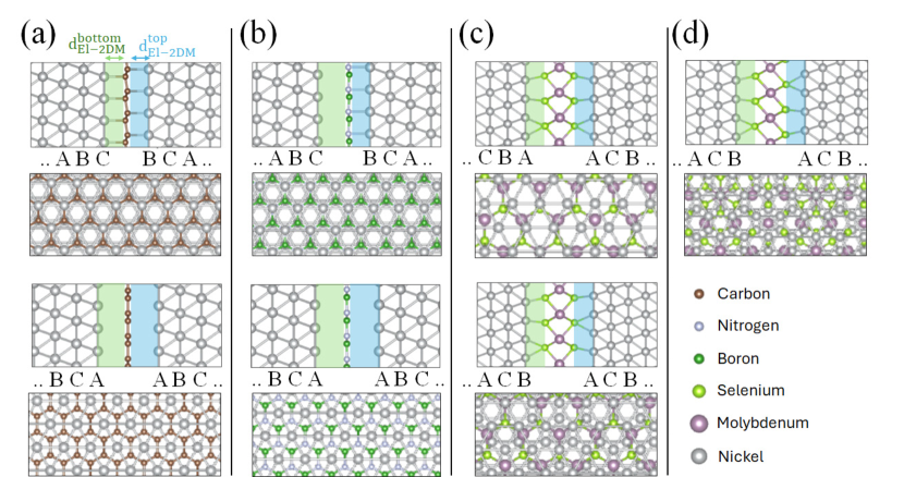
Figure 1 shows the relaxed structures of the heterostructures Ni2D materialNi, where the 2D material can be Gr, hBN, 2H-MoSe2 and 1T-MoSe2. The corresponding distances between the electrodes (), the top and bottom electrodes and the 2D material ( and , respectively), and the interaction energy are summarized in Tab. 1. Along the direction (111), Ni is composed of three layers (named A, B and C) with different stacking order and periodically repeated. The stacking modes of the heterojunctions are named according to the name of the Ni layers close to the 2D material, see Fig. 1. We have only considered two stacking modes among several possibilities for each 2D material, in order to discuss the significance of changing the layer stacking configuration. For graphene, see Fig. 1(a), the interfaces with the top and bottom electrodes are symmetric and exhibit an identical distance between the electrodes and the 2D material for the two stacking modes, i.e., . In CB stacking mode, the system exhibits a higher interaction energy and shorter distances compared to those of stacking mode AA, because of the vertical alignment of C atoms with the closest Ni atoms. An analogous result is observed when the 2D material is hBN, see Fig. 1(b). In stacking mode AA, where B and N atoms are not aligned with Ni atoms, the distance is larger, the corrugation is less pronounced and the interaction energy is lower than in stacking mode BC. Here the interfaces are asymmetric, as hBN interacts more strongly with the top electrode where N atoms are vertically aligned with Ni atoms. In contrast, Ni/2H-MoSe2, see Fig. 1(c), shows trivial changes depending on the stacking mode, as the Se atoms experience nearly identical Ni surroundings when averaged over the unit cell, thus leading to a similar interaction with top and bottom electrodes. This behavior, explained in detail later in this section, is related to the larger supercell size. Hence, for the Ni/1T-MoSe2 interface, see Fig. 1(d), we considered only the BA stacking configuration.
| Properties | NiGrNi | NihBNNi | Ni2H-MoSeNi | Ni1T-MoSeNi |
|---|---|---|---|---|
| stacking mode | AA — CB | AA — CB | AA — BA | BA |
| (Å) | 2.85 — 2.08 | 3.02 — 3.02 | 2.26 — 2.25 | 2.19 |
| (Å) | 2.91 — 2.09 | 2.98 — 2.04 | 2.26 — 2.25 | 2.19 |
| (Å) | 5.77 — 4.40 | 6.01 — 5.15 | 7.93 — 7.91 | 7.89 |
| Interaction energy (meV/Å2) | 223 — 274 | 211 — 238 | 236 — 238 | 282 |
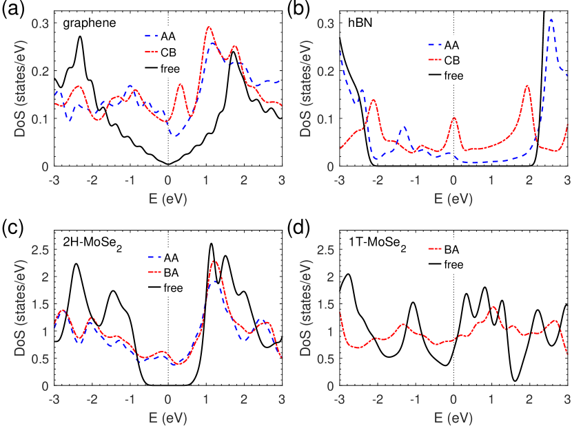
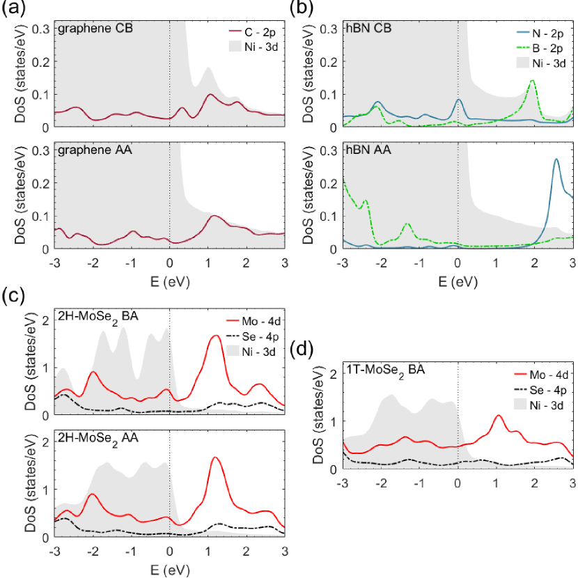
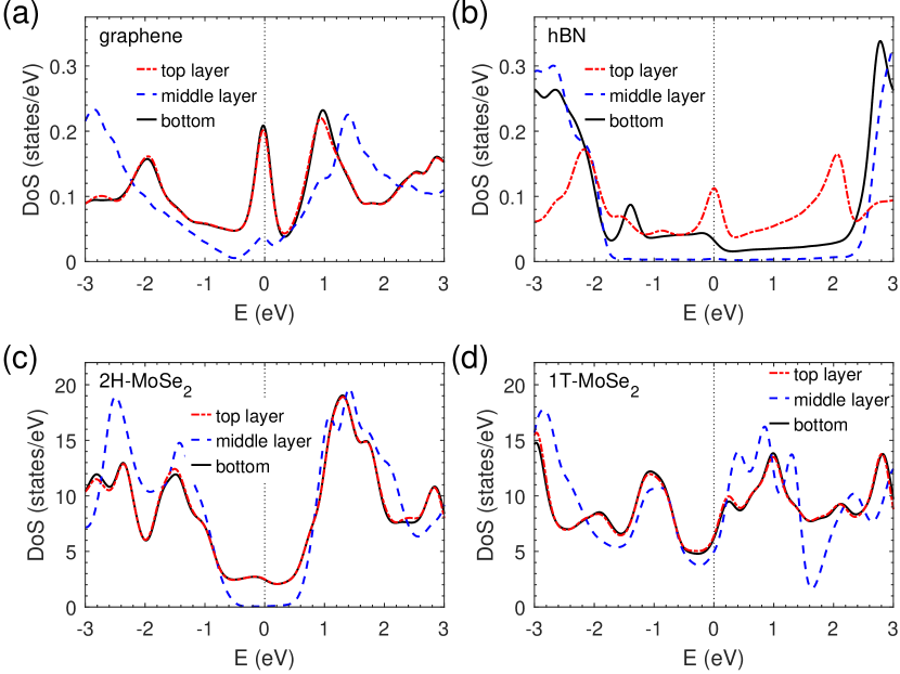
The stacking arrangement impact on the atomic interactions at the contacts is observed in the electronic properties, as illustrated in Fig. 2 by the total density of states (DoS), and in Fig. 3 by the projected DoS. The DoS of the Ni atom plane closest to the 2D material is also provided, with coinciding peaks proving the hybridization of their orbitals. In the case of graphene, see Fig. 2(a), the interaction between the C and Ni atoms, which are aligned in the CB stacking mode, results in significant modifications of the electronic structure of graphene. Indeed, graphene becomes fully metallic as a result of the strongly hybridized states at the interface with the contacts. From Fig. 2(b), for the CB stacking mode, the DoS exhibits states within the bandgap of hBN. This is consequence of the orbital hybridization between the states of N atoms and the states of Ni atoms, as clearly visible in the top panel of Fig. 3(b), from the N DoS peak at the Fermi level. This finding is consistent with the previous observations that, based on interface distances, the N-Ni interaction is stronger than the B-Ni interaction, due to the higher electronegativity of N atoms compared to B atoms. On the other hand, in the stacking mode AA, the hBN/Ni interface exhibits a weaker interaction, which can be seen from the reduced impact on the hBN DoS see Fig. 2(b) and Fig. 3(b). These observations highlight the critical importance of atomic alignment in tuning the structural and electronic properties at interfaces, thus emphasizing the potential to engineer specific electronic characteristics through precise control of stacking configurations. For MoSe2, see Fig. 2(c,d), both phases experience significant changes due to the interaction with the electrodes at the interface. More importantly, similarly to hBN, 2H-MoSe2 loses its semiconducting behavior due to state hybridizations with Ni at the interfaces, thus leading to induced electronic states within the bandgap. As expected, Fig. 2(c) shows that the electronic properties exhibit less pronounced dependence on the stacking mode for 2H-MoSe2. The DoS remains relatively unchanged for the two stacking modes, which can be attributed to the use of a larger supercell composed of different numbers of unit cells of different materials, as 2H-MoSe2(33)/Ni(44), see Fig. 1(c). This results in a larger variety of relative atomic positions within the supercell and then in an arrangement in which the interfacial interactions are strong in some areas and weak in others, regardless of the stacking mode. Consequently, the variations in stacking mode entail compensated interactions, which remain nearly similar for different stacking modes, when averaged over the supercell. This is in contrast with the cases of graphene and hBN, where smaller unit cells lead to direct contacts or weak interactions based on vertical alignment, see Fig. 1(a,b). Therefore, the trivial changes observed in the electronic properties of 2H-MoSe2 with varying stacking modes arise from its differing interfacial environment, in addition to the fact that coupling between Se and Ni atoms is weaker than the N-Ni coupling discussed above. On the other hand, 1T-MoSe2 keeps its metallic nature, see Fig. 2(d). In what follows, only energetically favorable stacking modes are considered for each heterostructure, which, according to the interaction energies reported in Tab. 1, are CB for graphene and hBN, and BA for MoSe2.
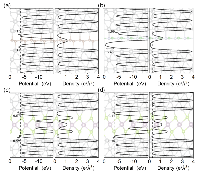
To further elucidate the electronic behavior at the interface level, Fig. 4 provides the in-plane-averaged charge distribution and the Hartree potential along the orthogonal axis, which explain the simulated conductivity reported in Tab. 2. Figure 4(a,c,d) shows that graphene and MoSe2, exhibit a symmetric charge distribution at the top and bottom interfaces. The effective potential shows a reduced tunnelling barrier at the interfaces with a higher charge accumulation and stronger interaction. In particular, graphene exhibits the lowest tunnelling barrier, which facilitates electron transfer across the interface and increases the transmission probability, thereby enhancing the overall conductivity of the system. Accordingly, the highest electrical conductivity is observed in the NiGrNi structure, due to the minimal tunnelling barrier. For the hBN/Ni interface, see Fig. 4(b), the interaction with the top electrode, where N-Ni bonding occurs, shows a charge density higher than at the bottom interface. This arises from the interaction of N atoms with Ni atoms, which is stronger than that of B atoms with Ni atoms, thus resulting in an asymmetric charge distribution. The lowest electrical conductivity of the NihBNNi heterostructure results from the highest tunnelling barrier at the interface dominated by the weaker B-Ni interaction.
Indeed, based on our results, the vertical transmission and the trend of the conductivity is related to the heights of the tunnel barriers, 2D material DoS at Fermi level, the distance between the electrodes and the 2D material, as well as its thickness. The high conductivity in graphene is consistent with its low tunnelling barrier, as mentioned above, and increased DoS, which enhances the electron transmission across the interface. In addition, the short supports stronger interface coupling and facilitates charge transfer. Compared to graphene and despite having close tunnelling barrier heights, the lower conductivity through 1T-MoSe2 may be attributed to its larger thickness. The 2H-MoSe2 configuration shows slightly lower conductivity ( S/) than 1T-MoSe2, due to its approximately 0.4 eV higher tunnelling barriers while having almost the same thickness and relatively close state densities at the Fermi level. Finally, despite being thinner than MoSe2, hBN shows the lowest conductivity, due to the significantly higher tunnelling barrier of 3.43 eV. The explanation can be found in the asymmetric tunnelling barriers, with one barrier being very high, thus suggesting that electron transmission is significantly blocked at one interface, thus resulting in reduced overall conductivity.
We observe significant modifications in the electronic characteristics of all 2D materials studied, due to their interaction with non-passivated electrodes. In particular, they become metallic when they previously were semiconducting or insulating. As a consequence, the transmission and electrical conductivity of their heterostructures are not intrinsically based on the electronic properties of the isolated materials. In the next section, we consider multilayer 2D materials to observe the impact of the intrinsic electronic properties on the electrical conductivity.
| Heterostructures | NihBNNi | Ni2H-MoSeNi | Ni1T-MoSeNi | NiGrNi |
|---|---|---|---|---|
| conductivity (S/Å2) | 1.33 | 1.88 | 1.95 | 3.27 |
3.2 Electronic and transport properties of Ni(111)multilayer 2D materialNi(111) heterostructures
| conductivity | NiGrNi | NihBNNi | Ni2H-MoSeNi | Ni1T-MoSeNi |
|---|---|---|---|---|
| ML (S/Å2) | 3.27 | 1.33 | 1.88 | 1.95 |
| 2L (S/Å2) | 0.48 | 0.20 | 0.06 | – |
| 3L (S/Å2) | 7.010-3 | 2.010-3 | 2.010-3 | 0.24 |
| 4L (S/Å2) | 1.410-4 | 9.410-5 | 5.810-5 | – |
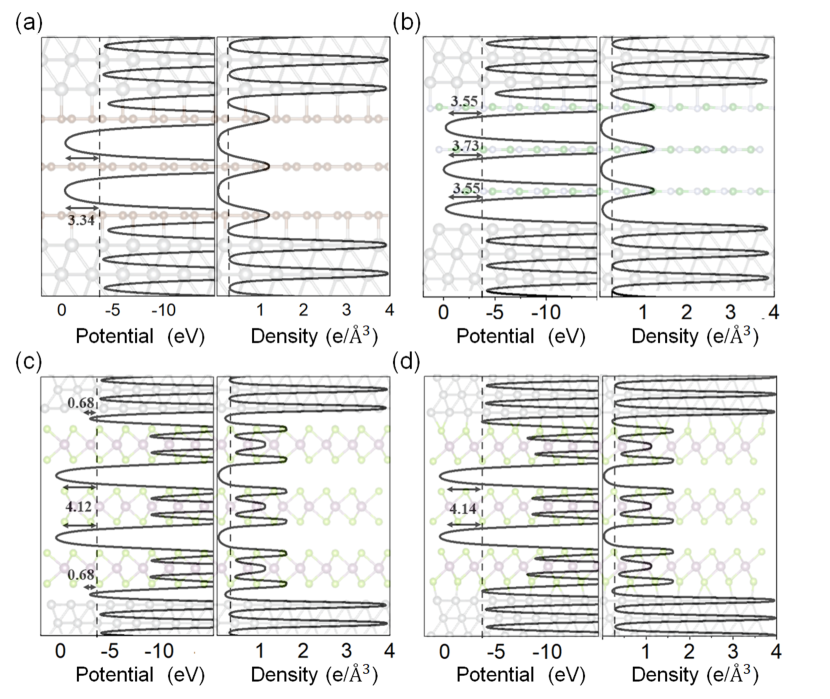
In this section, we consider multilayer 2D materials, among which, trilayers represent the thinnest multilayer structure that distinguishes the behavior between the middle layer and the layers close to the metallic contacts. This approach allows us to examine the individual contributions of the interfacial layers and the non-interacting middle layer, to the electronic and transport properties of the system as a whole. The corresponding DoS of our heterostructures with different numbers of 2D-material layers is reported in Fig. 5. The figure shows the DoS projection on the different layers of a trilayer, which reveals significant differences in their electronic structure. For all four 2D materials investigated, the layer in direct contact with the electrodes exhibits electronic characteristics similar to those in the monolayer cases, due to strong orbital hybridization with the metal atoms at the interface. For graphene, 2H-MoSe2 and 1T-MoSe2, due to the symmetric top and bottom layers-electrode distances, i.e., , the DoS is the same on the top and bottom layers, except for small numerical errors, see Fig. 5(a,c,d). For hBN, the different layers-electrode distances, with , entail a difference between the DoS in the top and bottom layers. In fact, as shown in Fig. 5(b), the stronger bond between the top electrode and the hBN layer, evidenced by the peak at the Fermi energy, leads to a greater DoS than that on the bottom layer. In contrast, the middle layer, see Fig. 5, is significantly less influenced by the metallic contacts and preserves its intrinsic electronic structure. This limited interaction allows the middle layer to maintain characteristics closer to its isolated form, apart from an energy shift induced by doping due to the charge transfer. In fact, as presented in Fig. 6, the reduced potential barrier and increased charge density are located only at the 2D material/Ni interface. In contrast, the interfaces between the 2D material layers show no significant charge density accumulation and exhibit high tunnelling barriers, which highlights the role of the middle layer in reducing the tunnelling current through the heterostructure. Then, the 2D contact layers act as passivating layers for the metallic contacts. As a result, the conductivity, see Tab. 3, decreases when increasing the number of layers. This trend is consistently observed over all the studied 2D materials. The trilayer 1T-MoSe2 shows a significantly higher conductivity value compared to the other 2D materials, which is due to its higher DoS at the Fermi level, especially in the middle layer, see Fig. 5(d). This contrasts with the semiconducting behavior of its 2H counterpart and hBN. These findings highlight the critical role played by the intrinsic electronic properties of 2D material in the overall transport behavior in multilayered 2D material systems. In the case of semiconducting 2D materials, we expect the conductivity to go to zero when increasing the thickness. In the case of metallic 2D materials, we expect the conductivity to saturate to a finite limit, mostly determined by the interlayer coupling and lower than its in-plane counterpart. In any case, according to our results, the conductivity is not strictly zero even with four layers and, with three layers, it is still much higher than experimentally observed [9]. This suggests the presence of important experimental characteristics not considered here, such as multilayer regions, polymer residues, or metal oxidation, which could bring the system deeper into the tunnelling regime and suppress its conductivity by orders of magnitude.
4 Conclusion
This work demonstrates the influence of stacking configurations and material thickness on the electronic and transport properties of metal2D materialmetal systems. In monolayer configurations, strong interactions with metal electrodes result in largely altered electronic states with the formation of gap states. However, in trilayer systems, the middle layer maintains its intrinsic properties due to the limited electrode interaction. Among the systems studied, graphene exhibits the highest conductivity due to its low tunnelling barrier and increased DoS at the Fermi level, while hBN exhibits minimal conductivity due to its high tunnelling barrier. We conclude that the out-of-plane transport characteristics are not directly related to the in-plane ones. In particular, a single hBN monolayer within non-passivated metallic contacts turns out to be conductive, despite its insulating nature when isolated. Our findings are of particular relevance for the use of 2D materials in the field of beyond CMOS electronics, with a specific emphasis on the development of atomristors.
Acknowledgements
This work is supported by the ANR SWIT project (ANR-19-CE24-0004) and the LabEx Minos (ANR-10-LABX-55-01). It is implemented using HPC resources from GENCI–IDRIS (Grant 2023 A0140914157), GENCI-TGCC (Grant 2024 A0160914157) and the GRICAD infrastructure (https://gricad.univ-grenoble-alpes.fr), which is supported by Grenoble research communities.
Appendix
| Devices | NihBNNi | Ni2H-MoSeNi | Ni1T-MoSeNi | NiGrNi |
|---|---|---|---|---|
| SIESTA K-grid | 20203 | 551 | 661 | 20203 |
| TRANSIESTA K-grid | 40401 | 10101 | 12121 | 40401 |
| TBtrans K-grid | 80801 | 25251 | 24241 | 80801 |
| R-grid (Ry) | 1000 | 1000 | 1000 | 1000 |
| Material | Ni | hBN | 2H-MoSe2 | 1T-MoSe2 | Gr |
|---|---|---|---|---|---|
| Basis size | DZDP | DZP+3s+3p nP | DZ + 4f P | DZP + 4f P | DZP+3s+3p nP |
| Energy shift (meV) | 110 | 110 | 70 | 70 | 90 |
| Splitnorm | 4s:0.6 | N2s:0.5 | 5s:0.6 | 5s:0.4 | 2s:0.25 |
| 3d:0.15 | N2p:0.5 | 4d:0.1 | 4d:0.25 | 2p:0.2 | |
| B2s:0.5 | 3s:0.05 | 3s:0.35 | |||
| B2p:0.5 | 3p:0.3 | 3p:0.35 | |||
| (Bohr) | B3s,p:9.5 | 3s:9 | |||
| (Bohr) | N3s,p:8.0 | 3p:9 | |||
| Orbitals | 22 | 34 | 59 | 62 | 34 |
| Properties | NihBNNi | Ni2H-MoSe2Ni | Ni1T-MoSe2Ni | NiGrNi |
|---|---|---|---|---|
| Supercell | 11 | 34 | 34 | 11 |
| Strain 2D (%) | 0.56 | 0.03 | 0.0 | 0.06 |
| Strain Ni (%) | 1.40 | 0.44 | 0.16 | 0.27 |
References
References
- [1] IEEE International Roadmap for Devices and Systems 2023 Beyond CMOS and Emerging Materials Integration
- [2] Avci U E, Morris D H and Young I A 2015 IEEE Journal of the Electron Devices Society 3 88–95
- [3] Robinson J A 2018 APL Materials 6 058202
- [4] Briggs N, Subramanian S, Lin Z, Li X, Zhang X, Zhang K, Xiao K, Geohegan D, Wallace R, Chen L Q, Terrones M, Ebrahimi A, Das S, Redwing J, Hinkle C, Momeni K, van Duin A, Crespi V, Kar S and Robinson J A 2019 2D Materials 6 022001
- [5] Dragoman M and Dragoman D 2021 Atomic-Scale Electronics Beyond CMOS (Springer International Publishing) ISBN 9783030605636
- [6] Hao Z, Yan Y, Shi Y and Li Y 2022 The Journal of Physical Chemistry Letters 13 1914–1924
- [7] Cresti A 2023 Beyond-CMOS: State of the Art and Trends (Wiley) ISBN 9781394228713
- [8] Lemme M C, Akinwande D, Huyghebaert C and Stampfer C 2022 Nature Communications 13 1392
- [9] Ge R, Wu X, Kim M, Shi J, Sonde S, Tao L, Zhang Y, Lee J C and Akinwande D 2017 Nano Letters 18 434–441
- [10] Kim M, Ducournau G, Skrzypczak S, Yang S J, Szriftgiser P, Wainstein N, Stern K, Happy H, Yalon E, Pallecchi E and Akinwande D 2022 Nature Electronics 5 367–373
- [11] Hus S M, Ge R, Chen P A, Liang L, Donnelly G E, Ko W, Huang F, Chiang M H, Li A P and Akinwande D 2020 Nature Nanotechnology 16 58–62
- [12] Shah A A, Kumar J, Dar A B and Shrivastava M 2023 IEEE Transactions on Electron Devices 70 6622–6629
- [13] Shah A A, Dar A B and Shrivastava M 2024 npj 2D Materials and Applications 8 80
- [14] Mitra S and Mahapatra S 2024 npj 2D Materials and Applications 8 26
- [15] Sangwan V K, Jariwala D, Kim I S, Chen K S, Marks T J, Lauhon L J and Hersam M C 2015 Nature Nanotech 10 403–406
- [16] Chen H, Kang Y, Pu D, Tian M, Wan N, Xu Y, Yu B, Jie W and Zhao Y 2023 Nanoscale 15 4309–4316
- [17] Sangwan V K, Lee H S, Bergeron H, Balla I, Beck M E, Chen K S and Hersam M C 2018 Nature 554 500–504
- [18] Wang M, Cai S, Pan C, Wang C, Lian X, Zhuo Y, Xu K, Cao T, Pan X, Wang B, Liang S J, Yang J J, Wang P and Miao F 2018 Nature Electronics 1 130–136
- [19] Jeong H Y, Kim J Y, Kim J W, Hwang J O, Kim J E, Lee J Y, Yoon T H, Cho B J, Kim S O, Ruoff R S and Choi S Y 2010 Nano Letters 10 4381–4386
- [20] Krishnaprasad A, Dev D, Han S S, Shen Y, Chung H S, Bae T S, Yoo C, Jung Y, Lanza M and Roy T 2022 ACS Nano 16 2866–2876
- [21] Zhang F, Zhang H, Krylyuk S, Milligan C A, Zhu Y, Zemlyanov D Y, Bendersky L A, Burton B P, Davydov A V and Appenzeller J 2019 Nature Matererials 18 55–61
- [22] García A, Papior N, Akhtar A, Artacho E, Blum V, Bosoni E, Brandimarte P, Brandbyge M, Cerdá J I, Corsetti F, Cuadrado R, Dikan V, Ferrer J, Gale J, García-Fernández P, García-Suárez V M, García S, Huhs G, Illera S, Korytár R, Koval P, Lebedeva I, Lin L, López-Tarifa P, Mayo S G, Mohr S, Ordejón P, Postnikov A, Pouillon Y, Pruneda M, Robles R, Sánchez-Portal D, Soler J M, Ullah R, Yu V W z and Junquera J 2020 The Journal of Chemical Physics 152 204108
- [23] Papior N, Lorente N, Frederiksen T, García A and Brandbyge M 2017 Computer Physics Communications 212 8–24
- [24] Perdew J P, Burke K and Ernzerhof M 1996 Physical Review Letters 77 3865–3868
- [25] Hamann D R 2013 Physical Review B 88 085117
- [26] van Setten M J, Giantomassi M, Bousquet E, Verstraete M J, Hamann D R, Gonze X and Rignanese G M 2018 Computer Physics Communications 226 39–54
- [27] Papior N, Brandbyge M and Calogero G 2018 Journal of Physics: Condensed Matter 30
- [28] Gonze X, Amadon B, Antonius G, Arnardi F, Baguet L, Beuken J M, Bieder J, Bottin F, Bouchet J, Bousquet E, Brouwer N, Bruneval F, Brunin G, Cavignac T, Charraud J B, Chen W, Côté M, Cottenier S, Denier J, Geneste G, Ghosez P, Giantomassi M, Gillet Y, Gingras O, Hamann D R, Hautier G, He X, Helbig N, Holzwarth N, Jia Y, Jollet F, Lafargue-Dit-Hauret W, Lejaeghere K, Marques M A L, Martin A, Martins C, Miranda H P C, Naccarato F, Persson K, Petretto G, Planes V, Pouillon Y, Prokhorenko S, Ricci F, Rignanese G M, Romero A H, Schmitt M M, Torrent M, van Setten M J, Van Troeye B, Verstraete M J, Zérah G and Zwanziger J W 2020 Computer Physics Communications 248 107042