[1]\fnmAnia C. Bleszynski \surJayich
1]Department of Physics, University of California, Santa Barbara, Santa Barbara, California 93106, USA
2]Nanofabrication Facility, Department of Electrical and Computer Engineering, University of California, Santa Barbara, Santa Barbara, California 93106, USA
3]Department of Materials Science and Engineering, Stanford University, Palo Alto, CA 94305, USA
Scalable, nanoscale positioning of highly coherent color centers in prefabricated diamond nanostructures
Abstract
Nanophotonic devices in color center-containing hosts provide efficient readout, control, and entanglement of the embedded emitters. Yet control over color center formation – in number, position, and coherence – in nanophotonic devices remains a challenge to scalability. Here, we report a controlled creation of highly coherent diamond nitrogen-vacancy (NV) centers with nanoscale three-dimensional localization in prefabricated nanostructures with high yield. Combining nitrogen -doping during chemical vapor deposition diamond growth and localized electron irradiation, we form shallow NVs registered to the center of diamond nanopillars with wide tunability over NV number. We report positioning precision of \qty4\nano in depth and \qty46(1)\nano laterally in pillars (\qty102(2)\nano in bulk diamond). We reliably form single NV centers with long spin coherence times (average = \qty98\micro) and 1.8 higher average photoluminescence compared to NV centers randomly positioned in pillars. We achieve a 3 improved yield of NV centers with single electron-spin sensitivity over conventional implantation-based methods. Our high-yield defect creation method will enable scalable production of solid-state defect sensors and processors.
Main
Optically addressable solid-state spin defects are versatile tools for quantum-enhanced technologies[1, 2]. The photonic degree of freedom enables single-spin readout[3] and control[4, 5] and entanglement generation[6, 7]. Moreover, engineered nanophotonic structures can greatly enhance spin-photon interfaces, where customized structures such as cavities[8, 9, 10, 11, 12, 13], solid immersion lenses[14], metalenses[15], nanobeams [16, 10] or nanowires [17, 18] can be fabricated in the host material to increase collection efficiency[19], waveguide emitted photons[9] or Purcell-enhance photon emission[20, 21, 22, 23, 24, 25]. In particular, diamond color centers are readily interfaced with engineered photonic structures to provide these advanced functionalities [26, 27, 28, 29]. To realize efficient defect-photon interfaces, it is necessary to engineer a good spatial overlap between the optical mode of the nanostructured device and the defect. However, control over the formation of color centers in position and number, while maintaining reproducibly long spin coherence, remains an outstanding problem in realizing scalable fabrication of devices equipped with quantum-enhanced functionalities.
Conventionally, color centers are created via ion implantation prior to device fabrication. The implantation dosage is chosen to match a target number of defects per device, but placement is random in the nanostructures. Subsequently, in a time-intensive, low-yield, and hence nonscalable post-selection process, devices with defects at the ideal position (e.g., at the mode maximum of the optical field) are selected. Moreover, the properties of the selected defects can degrade during the subsequent device fabrication process, e.g., at the etching step[30]. Alternate approaches utilize highly specialized, home-built localized implantation techniques to spatially co-locate a defect and a nanostructure. Atomic force microscopy-assisted implantation[31, 32] and focused ion beam implantation[33] have demonstrated lateral confinement inside prefabricated nanostructures to . Recently, a patterning technique [34] involving implantation masks has shown lateral positioning precision in a nanopillar, though the technique is limited to nanopillar geometries.
However, implantation-based techniques have several drawbacks. Most critically, they suffer from collateral damage incurred during implantation (e.g., vacancy clusters) that adversely affect optical[35, 36] and spin properties[37, 38, 34] of nitrogen-vacancy (NV) centers. For instance, spin coherence times have been limited to less than 20 and \qty50\micro for of 10 and implanted NV centers, respectively[37, 34]. Damage is also exacerbated at higher implantation dosages[38], which are necessary for, e.g., achieving high defect densities or ensuring the presence of a defect in a small target volume. Further, the spread in the depth of implanted defects hinders their precise vertical positioning. For example, implanted NV centers have a vertical spread of \qty14\nano due to implantation straggling[39] and ion channeling[40], effects that become even more severe at higher implantation energies.
In contrast to ion implantation, nitrogen -doping during chemical vapor deposition (CVD) diamond growth enables NV formation with reproducibly long spin coherence, nanometer-scale depth confinement even at large depths, and independent tunability over a wide range of nitrogen and NV densities[41, 42, 43, 44, 45]. Previous studies on -doped CVD-grown diamond demonstrated NV center densities tunable from 1 to \qty47\unitppm ⋅\nano using electron irradiation[46, 41, 42], depth confinement, and reproducibly long coherence times, with even \qty15\nano-deep NVs showing \qty100\micro[47]. Depth confinement of NV centers using -doping has been used to enhance their coupling to nanophotonic devices, such as photonic crystal nanobeam cavities[48], but without controlled lateral positioning. Local vacancy creation techniques [49, 50, 51, 52, 53, 54] can also provide lateral confinement in addition to the depth confinement afforded by -doping, but this capability has only been demonstrated on a bulk substrate without alignment to prefabricated photonic structures [44, 46].
In this paper, we demonstrate high-throughput, localized formation of highly coherent NV centers aligned to prefabricated nanophotonic structures. We register a \qty200\kilo electron beam with \qty20\nano spot size, which we call -electron irradiation, to the center of diamond nanopillars fabricated in CVD-grown diamond with a \qty53\nano-deep, -doped nitrogen layer. By controlling the electron dose and annealing time, we tune the average number of NVs per irradiation spot inside nanopillars from to 10. We report lateral confinement of created NVs to a standard deviation of in unpatterned diamond in addition to \qty4\nano vertical confinement. Lateral confinement is improved to \qty46(1)\nano in 280 nm diameter pillars and \qty72(1)\nano in 480 nm diameter pillars. We find that our observations agree well with Monte Carlo (MC) simulations based on a simple diffusion-capture model. Importantly, the NVs formed using our method feature repeatably long spin coherence time (average = \qty98 (37)\micro) with a high spin-dependent photoluminescence () contrast of \qty18 (4). Additionally, we observe a 1.8 enhancement of from NV centers localized to pillars compared to pillars with non-localized NVs. Lastly, we demonstrate increase in the expected yield of single electron spin-sensitive magnetometers compared to conventional methods. Overall, this technique facilitates the scalable fabrication of state-of-the-art solid-state defect-assisted devices, where scalable refers to a high-yield, time-efficient process that leverages commercially available tools.
Targeted formation of NVs in nanostructures
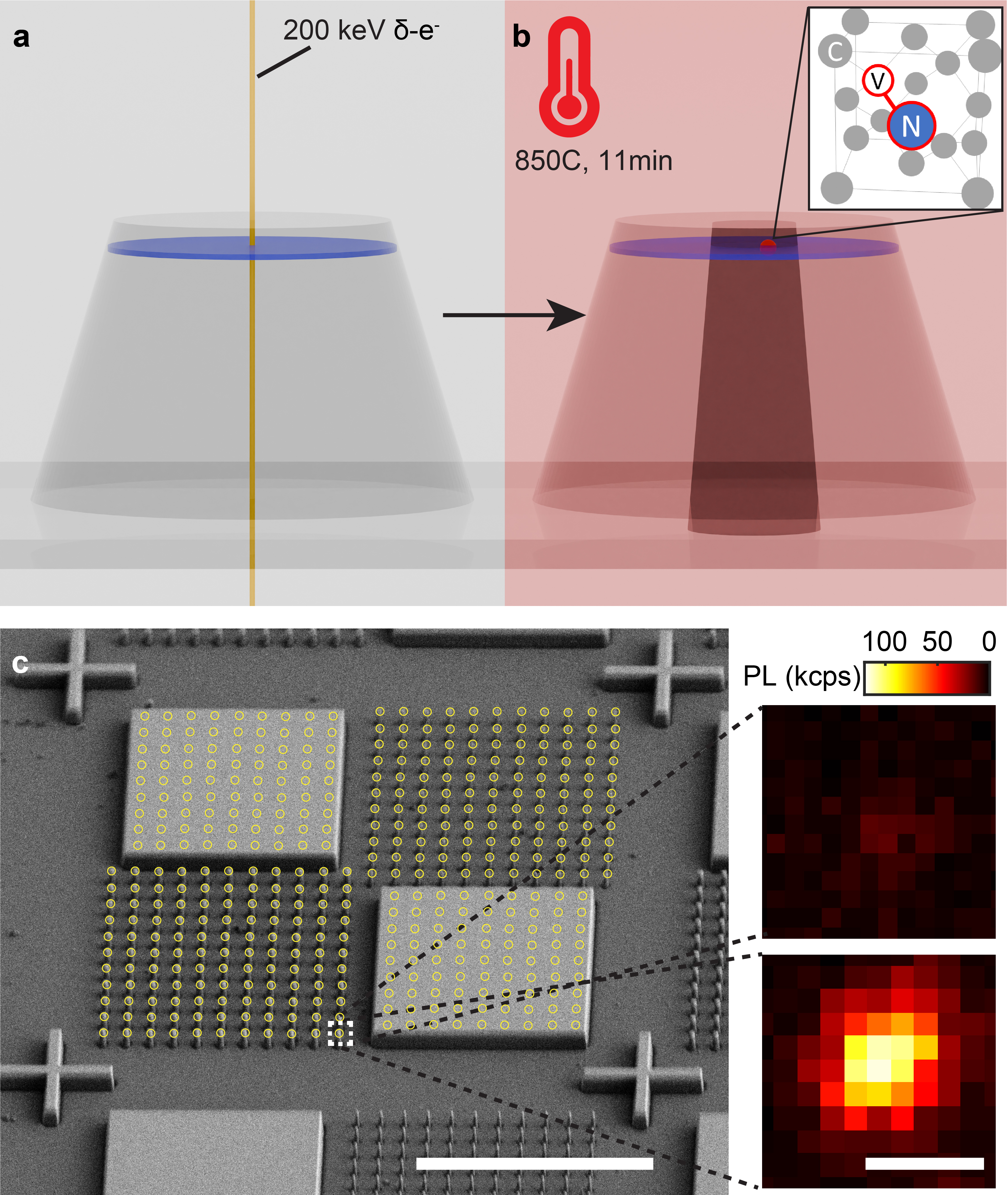
Our targeted formation of NVs in prefabricated nanostructure utilizes localized electron irradiation and timed vacuum annealing, as shown schematically in Figure 1(a-b). We first fabricate our device from a CVD-grown diamond with a \qty53\nano-deep 15N -doped layer, as described in Methods [41]. We use electron beam lithography (EBL) followed by inductively coupled plasma-reactive ion etching (ICP-RIE) recipes to transfer nanostructures onto the diamond substrate. We use a negative electron beam resist (FOx-16, Dow Corning) as a mask for etching tall features with Ar/O2 plasma. Nanopillars with diameters \qty280\nano and \qty480\nano, square mesas with \qty20\micro \qty20\micro dimensions, and alignment marks were fabricated, as shown in the scanning electron micrograph (SEM) in Figure 1(c).
To laterally localize NV centers, we use a commercially available \qty200\kilo EBL tool (JBX-8100FS, JEOL Ltd.) to -electron irradiate the centers of the nanopillars using an electron beam of \qty20\nano spot size (Figure 1(a)); these electrons can penetrate into the diamond and displace carbon atoms along their trajectory up to below the surface[55, 46], creating a narrow pencil of vacancies(Figure 1(a), SI). We note that \qty145\kilo is the threshold energy for vacancy creation in diamond [46] and only recently have commercial EBL tools exceeded \qty150\kilo. The resulting monovacancy density depends on electron dose, which we tune from \qty1.6e19^-\per\centi\squared to \qty4.8e21^-\per\centi\squared by adjusting the dwell time while keeping the beam current constant at \qty20\nano. Subsequent annealing at \qty850 for 11 minutes in vacuum promotes the diffusion of monovacancies (Figure 1(b)). When a monovacancy diffuses to a site adjacent to a nitrogen atom, it can get captured to form an NV center (Figure 1(b), inset). We note that NVs formed in the -doped N-layer can be identified by their 15NV hyperfine structure, revealed with pulsed electron spin resonance (ESR) spectroscopy. Then, the device is cleaned in a boiling nitrating acid (1:1 HNO3:H2SO4) and annealed at \qty450 in air. All NV measurements were taken using a home-built confocal microscope with \qty532\nano excitation[56].
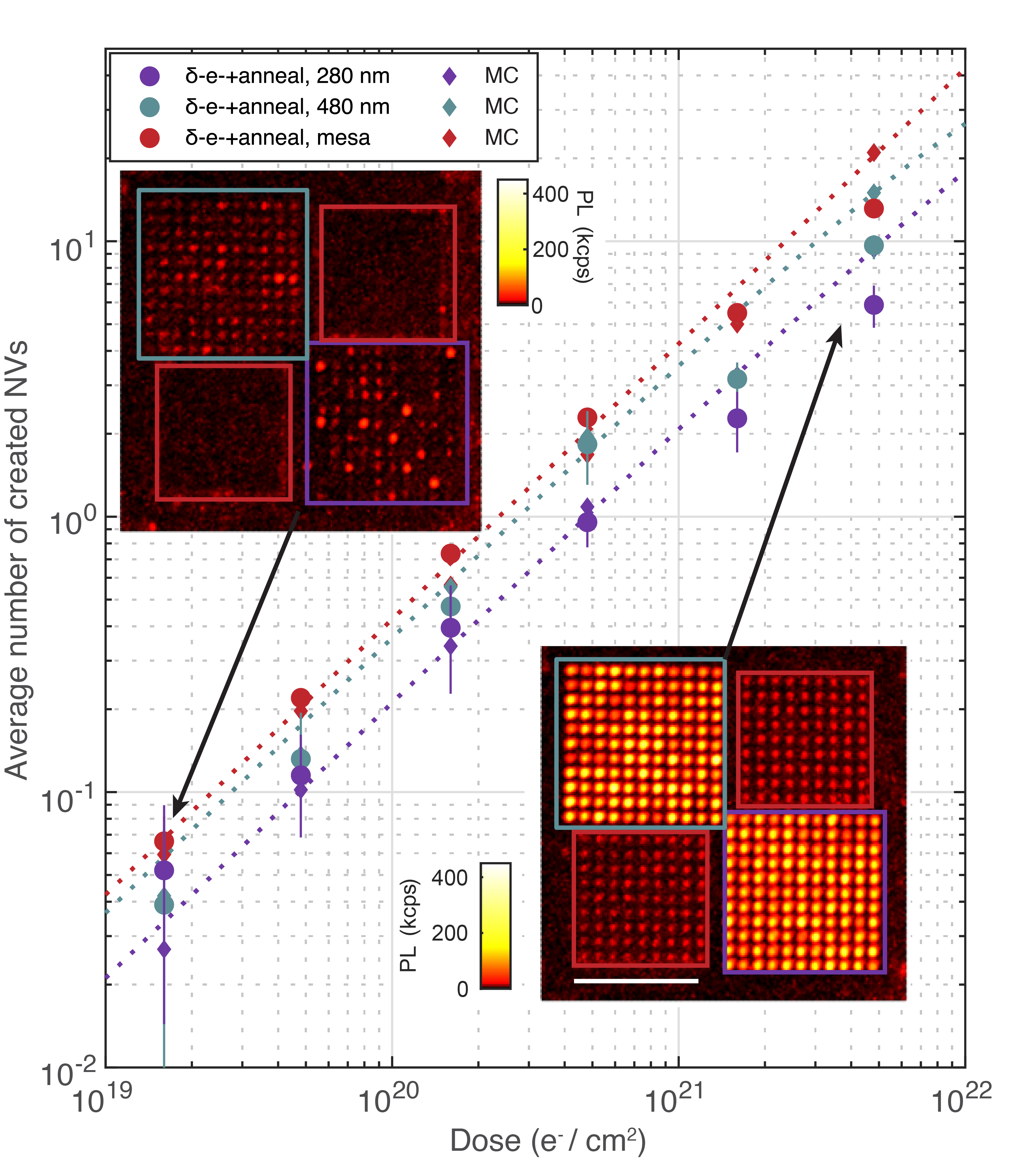
First, we show control over the number of NVs formed per nanopillar by varying the -electron irradiation dosage. In Figure 2, we sweep the irradiation dose from \qty1.6e19^-\per\centi\squared to \qty4.8e21^-\per\centi\squared and measure the average number of NVs created in \qty280\nano (purple circles) and \qty480\nano (teal circles) diameter pillars. We use a maximum likelihood estimation (MLE) method [46] based on continuous wave-ESR spectroscopy (CW-ESR) taken on 121 pillars for each pillar size and irradiation dose after annealing (details in SI). With increasing irradiation dose, the average number of created NVs increases monotonically from to 5.9(7) and 9.7(4) for \qty280\nano and \qty480\nano diameter pillars, respectively. We subtract the contribution from as-grown NVs, characterized by measuring non-irradiated pillars of each diameter (see SI). We also estimate the average NV number per spot in -electron irradiated mesas by measuring the total around the target areas normalized by that of single NVs, as plotted in red circles in Figure 2. Likewise, we observe a monotonic increase in the NV formation with irradiation dose.
The increase in NV number with pillar diameter indicates that vacancies diffuse at least as far as the radius of the smaller pillar, and comparing our results to Monte Carlo (MC) simulations (Methods) of a simple diffusion-capture model of NV formation, we extract a monovacancy diffusion constant \qty17(4)\nano\squared\per (see SI). Simulation results are plotted as diamonds in Figure 2. At higher irradiation doses, () simulations slightly overestimate NV number, which we attribute to the creation of vacancy clusters at high monovacancy density[57, 58, 59], giving rise to sublinear monovacancy creation efficiency. In the next section, we characterize via an alternate approach, arriving at a similar value, and we further discuss the results.
We identify \qty5e20^-\per\centi\squaredand \qty3e20^-\per\centi\squared as the target dose for an average of 1 NV per \qty280\nano and \qty480\nano pillar, respectively, facilitating the fabrication of devices based on single isolated defects for sensing and networking applications. We expect the target electron dose to vary for different nitrogen densities and nanostructure geometries.
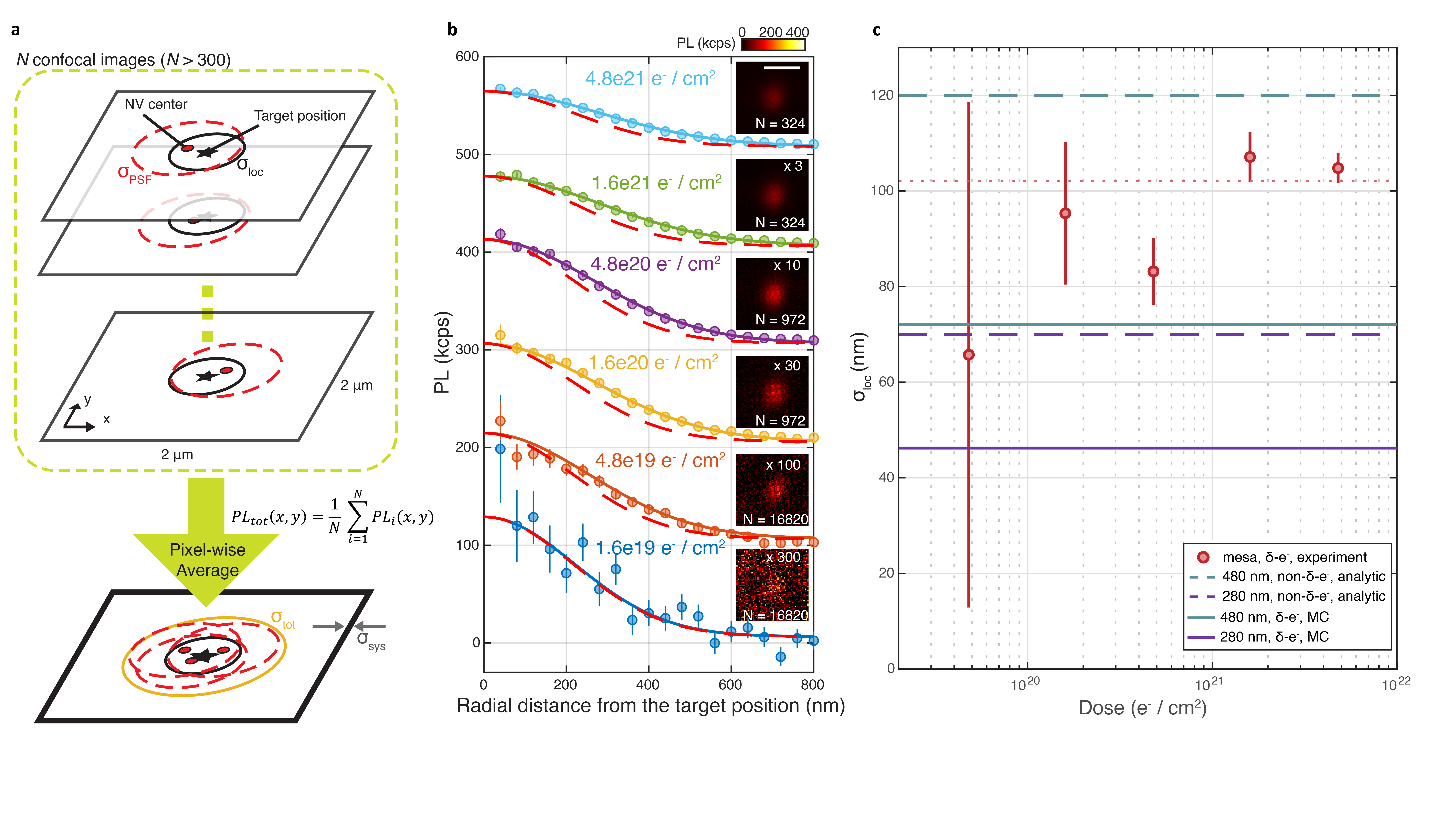
We next demonstrate high spatial confinement of NV centers aligned to diamond nanostructures, which is necessary for optimizing spatial overlap between the defect qubit and the structure’s photonic modes. In Figure 3, we quantify the lateral positioning precision of created NVs afforded by -electron irradiation. To do so, we first investigate arrays of NVs patterned in \qty20\micro\squared mesas and quantify the deviation of NV positions from their target irradiation spot. The irradiation pattern on the mesa is shown in yellow circles in Figure 1(c) and example confocal images are shown in Figure 2 (bottom right and top left square of each inset). We use these featureless mesas to avoid exciting photonic modes of the nanopillars that modify the NV emission pattern and obfuscate the actual NV position. We estimate , the standard deviation of lateral NV positioning in the mesas, by pixel-wise averaging 162 tiles in the confocal image, with each \qty2\micro\squared tile centered on a single irradiation spot; the tiles were obtained by cutting a 40 confocal image containing two mesas (the area shown in Figure 1(c)) into a regular grid (see SI). Prior to this image cutting we apply global affine transformations to the original confocal image to account for optical aberrations in our imaging system. We then repeat this procedure over several different 40 confocal image areas to arrive at the pixel-wise averaged confocal images shown in the insets of Figure 3(b). Each of these images has a finite lateral spread with respect to the target positions due to three contributions: the lateral NV positioning precision of our patterning technique , the point spread function (PSF) of our imaging system , and residual global aberrations not removed after the first set of global affine transformations :
| (1) |
To extract we first measure by fitting the averaged confocal images with a 2D Gaussian curve,
| (2) |
where is the maximum of the averaged confocal image. The radial profiles of the averaged images (circles) and the fits (solid lines) are shown in Figure 3 (b). Then, we measure by imaging six single NVs in the mesa region, as described in [41]. We characterize the residual global aberration of our transformed images to be \qty41\nano (see SI). Finally, we extract for the different irradiation dosages and plot the results in Figure 3(c) (red circles). The data shows minimal dependence of on dose, with an average = \qty102(2)\nano (red dotted line).
We attribute the majority of to vacancy diffusion during annealing, and hence our measured provides an estimate of via comparison with MC simulations (see SI). This number is consistent with the estimated from NV number measurements (Figure 2) and is within the range of values reported in the literature. We note that reported values of show strong sensitivity to experimental conditions including annealing temperature, annealing time, and vacancy creation method [46, 60, 61, 62, 44]. For instance, Ref. [44] measured at \qty850-\qty30min annealing and Ref. [61] found at \qty1050-\qty2 annealing. Further, Ref. [62] found can be enhanced due to transient dynamics during the first few minutes of annealing ( for \qty2 annealing at \qty1000).
We next estimate the lateral NV positioning precision in the nanopillars . We use MC simulations because a direct measurement is challenging due to the effect of the pillars’ photonic modes on the confocal images. As shown in Figure 3 (c), (solid lines) is smaller than , and notably smaller than for NVs uniformly distributed in a nitrogen layer bounded by the pillar walls (where pillar diameter), as would result from the conventional method of forming pillars after NV formation. In contrast, our technique achieves improved lateral confinement even in pillars with comparable size to , a fact we attribute to vacancy absorption at the pillar sidewalls during annealing. Specifically, we find = \qty46(1)\nano and \qty72(1)\nano in our -electron irradiated \qty280\nano and \qty480\nano pillars. This improved lateral confinement is expected to enhance the coupling to the nanopillar photonic mode, as shown in the next section.
Spin and optical properties of single NVs in nanopillars
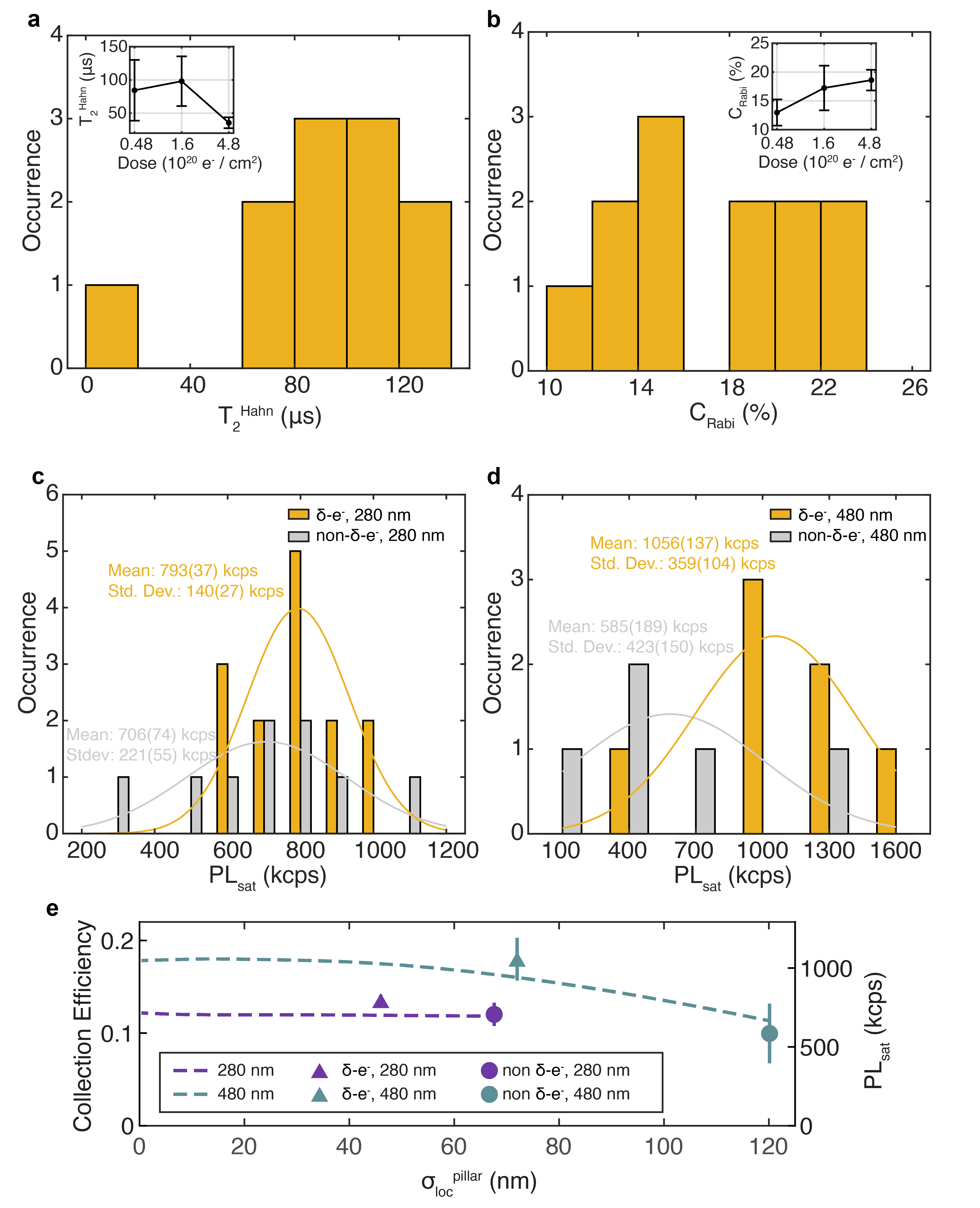
We next present the spin coherence and photoluminescence properties of single 15NV centers created inside nanopillars. Figure 4(a) shows a histogram of the Hahn echo coherence time, , of 12 NV centers formed by \qty1.6e20^-\per\centi\squared-irradiation. We observe reliably long with a mean of \qty98 (37)\micro, which we attribute to the gentle nature of our NV formation process, producing little collateral damage that can adversely affect coherence. The coherence time is consistent with the limit imposed by the surrounding substitutional nitrogen (P1 center) bath(see SI). In contrast, \qty15keV ion implantation results in NVs with the majority having less than \qty50\micro[34]. As shown in the inset, we also measure long for single NV pillars with \qty4.8e19^-\per\centi\squared irradiation, while we see a reduced of \qty36(8)\micro for \qty4.8e20^-\per\centi\squared (Figure 4(a), inset). We attribute this reduction to increased vacancy-related damage, consistent with previous reports [60, 41].
We also demonstrate favorable optical properties of our -electron irradiated single NV centers, namely good spin-dependent optical readout contrast and high photon collection rates. Fig. 4(b) shows an average spin-dependent Rabi contrast of \qty18(4) at \qty1.6e20^- \per\centi\squared, where and are the for NV electronic spin states 0 and , respectively . The inset shows the dependence of on irradiation dose with no evidence of reduced contrast at the highest dosages compatible with single NV formation.
In Figure 4(c) and (d), we show histograms (yellow) of the saturation count rate for \qty280\nano and \qty480\nano pillars, respectively, where is measured as a function of \qty532\nano excitation power (see SI). The means of the two histograms are 0.793(37) Mcps and 1.056(137) Mcps, respectively. Also plotted in grey are the histograms of non-irradiated pillars with as-grown single 15NVs, which have a uniform spatial distribution inside the pillars. The non-irradiated pillars show a lower mean compared to the -electron irradiated pillars by a factor of 1.8 and 1.1 for \qty480\nano and \qty280\nano pillars, respectively. The increase in mean in the -electron irradiated 480 nm pillars is statistically significant.
In Figure 4(e), we conduct finite-difference time-domain (FDTD) simulations to study the effect of lateral localization on in nanopillars (see Methods). The simulations (dashed lines) and the data are in good agreement, indicating that increased localization precision is the main contributor to increased for the \qty480\nano pillars, while does not depend strongly on in the 280 nm pillars. For both pillars, our nearly maximizes photon collection efficiency. For future applications, color center localization should be performed in conjunction with FDTD simulations to optimize the emitter overlap with the photonic mode. Overall, high collection efficiency combined with long coherence and large shown here is crucial for realizing advanced functionalities in devices for NV-based sensing, as discussed in the next section.
High-yield, scalable magnetic field sensors
Lastly, we present an outlook for the improvements our method offers to scalable, high-yield fabrication of highly sensitive magnetic field sensors.
In a typical optical spin-state readout scheme, the alternating current (AC) magnetic field sensitivity is given as
| (3) |
where is the reduced Planck constant, is the NV’s electronic g factor, is the Bohr magneton, is the total free evolution time, and is the average photon number per measurement. This expression highlights the importance of long , large , and high for sensing small magnetic fields.
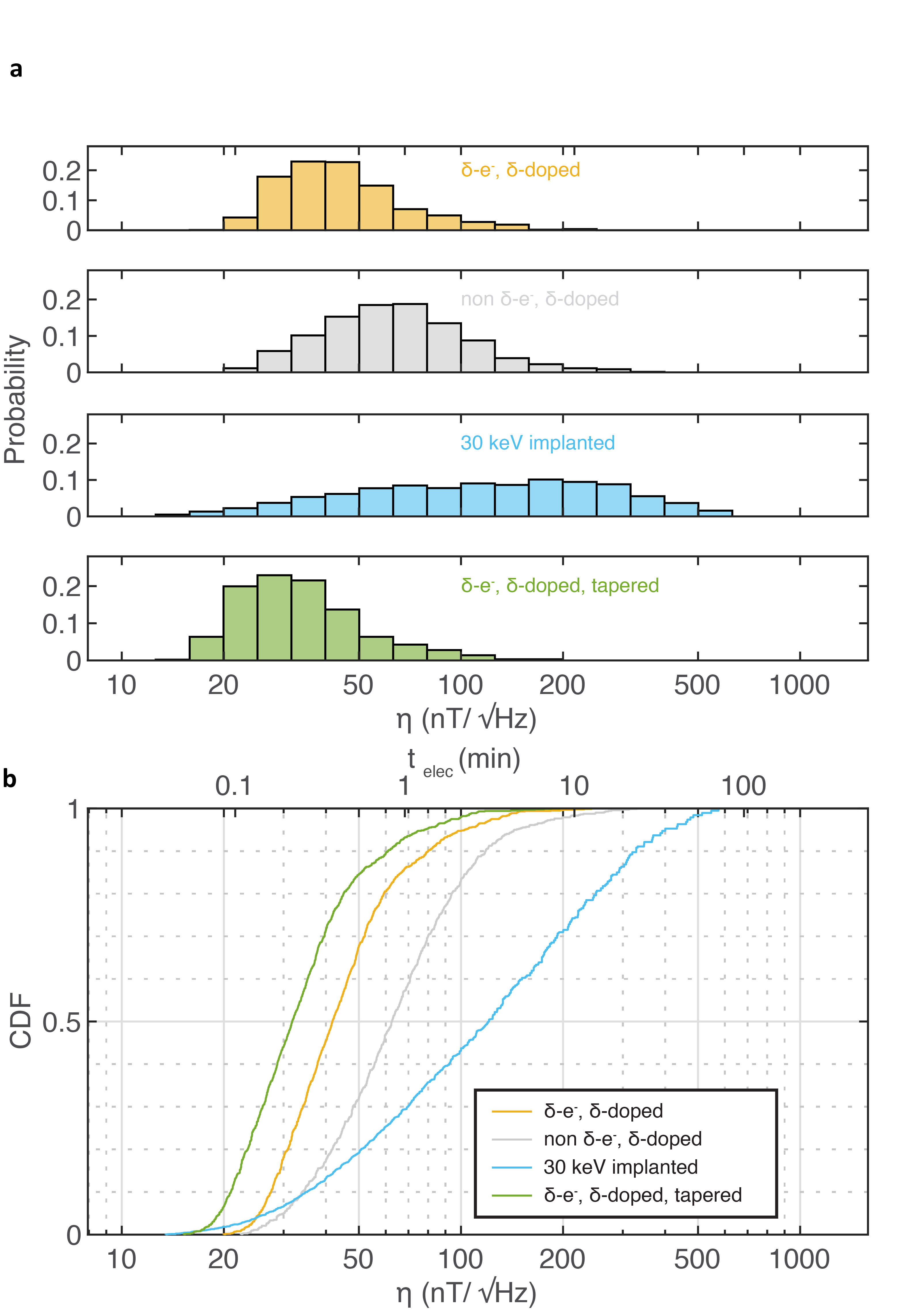
Figure 5(a) shows simulated histograms of for NVs in pillars formed via our method (yellow) compared to two other methods: conventional 30 keV nitrogen-implanted layers (cyan) and -doped layers without lateral localization (gray). Also plotted are -electron irradiated pillars with future improvements to the pillar geometry (green). The distributions are generated using Equation 3 with and with the , and distributions experimentally measured in this work. From this histogram, we calculate the cumulative density function in Figure 5 (b). The median of NVs formed using our method is \qty42\nano/ with \qty86 of the NV centers exhibiting . For reference, a 53-nm deep NV with can detect a single electron spin at the diamond surface in a typical averaging time of 1 minute. For the non-localized -doped method, the median is \qty63\nano/ with \qty57 of the NVs exhibiting , where we use the measured , , and distributions of non-irradiated pillars. With the conventional, implantation-based method, the median is \qty121\nano/ with \qty29 of the NVs exhibiting , where we use the measured and distributions from non-irradiated pillars with the reported distribution of from \qty30keV implantation[63], chosen because it produces a similar NV depth of 40-\qty50\nano. Hence our method produces a significantly higher yield of high-sensitivity NV magnetometers, where we demonstrate an estimated 3-fold higher yield of single-electron-spin detectable magnetometers compared to conventional implantation-based methods. We note that further improvements can be realized by utilizing pillars with a sidewall taper angle[34], as shown in green in Figure 5. Higher-order dynamical decoupling can also extend coherence time, where an order of magnitude increase for shallow, -doped NVs has been demonstrated [47], leading to a further 3 improvement in to .
Conclusions
To conclude, we demonstrate three-dimensional localized formation of highly coherent NV centers aligned to prefabricated nanophotonic structures. Using our method, we find NV spin and photoluminescence properties superior to those for NV centers formed via conventional implantation methods as well as nonlocalized -doped methods. These improved properties culminate in a significantly higher yield of high-sensitivity magnetometers, an important application of NV centers. Through our work, we also gain an understanding of vacancy diffusion in nanostructured diamond devices.
While we demonstrate our technique here on NV centers in diamond nanopillars, we emphasize that our method can be readily applied to other device geometries, such as 2D and 1D photonic crystal cavities [33, 24] and nano-optomechanical devices [64] as well as to other material systems, including divacancies[65] and silicon vacancies[66] in silicon carbide and T centers in silicon[67]. In these optically addressable qubit systems, the advantages outlined here can be transferred using a similar targeted irradiation technique guided by our model of vacancy diffusion and capture for different geometries.
Looking forward, there is still room for further improvement in the collective control over the number, position, and coherence of color centers. The ultimate goal of forming a single defect with unit probability at a spot can be achieved by, for instance, -electron irradiation with in-situ annealing and photoluminescence characterization. More accurate positioning can be achieved by reducing the annealing time and optimizing irradiation parameters (e.g., smaller spot size). Overall, our results strengthen the role of optically addressable solid-state spin defects in next-generation metrology and information science.
Methods
PECVD diamond growth
Diamond homoepitaxial growth and doping were performed via plasma-enhanced chemical vapor deposition (PECVD) using a SEKI SDS6300 reactor on a (100) oriented electronic grade diamond substrate (Element Six Ltd.). Prior to growth, the substrate was fine-polished by Syntek Ltd. to a surface roughness of 200-300 pm, followed by a 4-\qty5\micro etch to relieve polishing-induced strain. The growth conditions consisted of a 750 W plasma containing 0.1 12CH4 in 400 sccm H2 flow held at 25 torr and 730 ∘C according to a pyrometer. A 154 nm-thick isotopically purified (99.998 12C) epilayer was grown. During the nitrogen -doping period of growth, 15N2 gas \qty1.0 of the total gas content) is introduced into the chamber for five minutes. After growth, the sample was characterized with secondary ion mass spectrometry (SIMS) to estimate the isotopic purity, epilayer thickness, and properties of the -doped layer (3.6 nm thick, 98 ppm*nm, see SI).
Monte-Carlo simulations
We simulate NV center formation using Monte Carlo (MC) simulation. Our simulation models the dominant effects during the annealing step, namely the diffusion of monovacancies within the prefabricated device and their capture by the existing nitrogen atoms to form NV centers. We also consider vacancy recombination at the diamond surfaces [39, 68] (e.g., the top surface and the pillar’s sidewalls for nanopillars).
Simulating the atomic-scale diffusion process on a diamond lattice is computationally intensive, necessitating approximately 50 million discrete ”jumps” for a vacancy to traverse \qty1\micro, with each jump spanning a minuscule \qty0.154\nano C-C bond spacing. Therefore, we adopt a coarse-grained approach with a cubic lattice of spacing \qty1\nano, still significantly smaller than the device dimensions. Within each simulation run, we randomly select positions for nitrogen atoms within the -doped layer region and vacancies within the vacancy-rich area from \qty200\kilo electron irradiation. We estimate from CASINO simulations with a scaling factor , which is set as a free parameter (see SI). For computational efficiency, we only consider vacancies with depth (\qty1\micro) since deeper vacancies do not contribute to NV center formation.
Given the initial conditions of the simulations, we segment the annealing process into shorter time steps. In each step, all vacancies randomly move some number of jumps, after which we check if they encountered a capture event. A capture by a nitrogen atom can occur when a monovacancy is in the same coarse-grained cell as a nitrogen atom with a probability of , where and are the volumes of the coarse-grained cell and unit cell, respectively. When an NV center forms, both the vacancy and the nitrogen atom are removed from the simulation during the subsequent time steps. Conversely, if a monovacancy gets captured by the boundaries, only the vacancy is eliminated.
Finite-difference time-domain simulations
Lumerical FDTD software is used to simulate the collection efficiency of photons emitted by NVs inside nanopillars. We model an NV as a point source consisting of two orthogonal dipoles perpendicular to the NV axis. The emission frequency range of the dipole is chosen to match the frequency range of the phonon sideband of the NV emission spectrum at room temperature: . The NVs are positioned \qty53\nano below the top surface. We simulate our two nanopillar geometries with diameters \qty280\nano and \qty480\nano with the side wall angle of and height of \qty1.4\micro, which are attached to a diamond slab of finite thickness. For computational efficiency, we set the thickness of the slab to be \qty1\micro. To avoid any interference due to this relatively thin slab, we absorb all incoming fields at the bottom surface of the slab. We do this by setting the simulation area such that the bottom diamond interface matches the perfectly absorbing simulation boundary. The collection efficiency is then calculated from the power transmitted to a monitor plane just below the pillar inside the slab. We calculate the far-field emission through a collection cone with .
To calculate the mean collection efficiency for the distribution of NVs with a given , we first sweep the position of the NV laterally in two orthogonal directions ( and ) and calculate the collection efficiency. Then, we extrapolate the collection efficiency for a given radial displacement by assuming the superposition of two orthogonal NVs. In particular, the collection efficiency is calculated as a weighted average of those calculated at two orthogonal displacements and , where the weights are given as and , respectively. We sweep the lateral confinement of NVs from perfectly localized () to maximally delocalized ( pillar diameter, corresponding to a uniform lateral distribution across the pillar). For simplicity, we set the lateral probability distribution to follow a 2D Gaussian function with a spread of which we truncate at the pillar boundary beyond which the probability is zero. For a given , we use the probability distribution and simulated collection efficiency to calculate both and the mean of the collection efficiency.
1 Acknowledgments
The authors thank Hitoshi Kato and JEOL Ltd. for \qty200\kilo irradiation. We gratefully acknowledge the support of the Gordon and Betty Moore Foundation’s EPiQS Initiative via Grant GBMF10279. We also acknowledge support from Cooperative Research on Quantum Technology (2022M3K4A1094777) through the National Research Foundation of Korea(NRF) funded by the Korean government (Ministry of Science and ICT(MSIT)), and from the DOE Q-NEXT Center (Grant No. DOE 1F- 60579). The authors acknowledge the use of shared facilities of the UCSB Quantum Foundry through Q-AMASE-i program (NSF DMR1906325), the UCSB MRSEC (NSF DMR 1720256), the UCSB Nanofabrication Facility (an open access laboratory), and the Quantum Structures Facility within the UCSB California NanoSystems Institute. S. A. M and acknowledges support from UCSB Quantum Foundry. L. B. H. acknowledges support from the NSF Graduate Research Fellowship Program (DGE 2139319) and the UCSB Quantum Foundry.
References
- \bibcommenthead
- [1] Awschalom, D. D., Hanson, R., Wrachtrup, J. & Zhou, B. B. Quantum technologies with optically interfaced solid-state spins. Nature Photonics 12, 516–527 (2018). URL https://www.nature.com/articles/s41566-018-0232-2.
- [2] Wolfowicz, G. et al. Quantum guidelines for solid-state spin defects. Nature Reviews Materials 6, 906–925 (2021). URL https://www.nature.com/articles/s41578-021-00306-y.
- [3] Doherty, M. W. et al. The nitrogen-vacancy colour centre in diamond. Physics Reports 528, 1–45 (2013). URL https://www.sciencedirect.com/science/article/pii/S0370157313000562.
- [4] Yale, C. G. et al. All-optical control of a solid-state spin using coherent dark states. Proceedings of the National Academy of Sciences 110, 7595–7600 (2013). URL https://www.pnas.org/doi/full/10.1073/pnas.1305920110.
- [5] Hilser, F. & Burkard, G. All-optical control of the spin state in the NV- center in diamond. Physical Review B 86, 125204 (2012). URL https://link.aps.org/doi/10.1103/PhysRevB.86.125204.
- [6] Bernien, H. et al. Heralded entanglement between solid-state qubits separated by three metres. Nature 497, 86–90 (2013). URL https://www.nature.com/articles/nature12016.
- [7] Stolk, A. J. et al. Metropolitan-scale heralded entanglement of solid-state qubits (2024). URL https://arxiv.org/abs/2404.03723v1.
- [8] Tomljenovic-Hanic, S., Steel, M. J., Sterke, C. M. d. & Salzman, J. Diamond based photonic crystal microcavities. Optics Express 14, 3556–3562 (2006). URL https://opg.optica.org/oe/abstract.cfm?uri=oe-14-8-3556.
- [9] Lukin, D. M. et al. 4H-silicon-carbide-on-insulator for integrated quantum and nonlinear photonics. Nature Photonics 14, 330–334 (2020). URL https://www.nature.com/articles/s41566-019-0556-6.
- [10] Babin, C. et al. Fabrication and nanophotonic waveguide integration of silicon carbide colour centres with preserved spin-optical coherence. Nature Materials 21, 67–73 (2022). URL https://www.nature.com/articles/s41563-021-01148-3.
- [11] Bhaskar, M. K. et al. Experimental demonstration of memory-enhanced quantum communication. Nature 580, 60–64 (2020). URL https://www.nature.com/articles/s41586-020-2103-5.
- [12] Stas, P.-J. et al. Robust multi-qubit quantum network node with integrated error detection. Science 378, 557–560 (2022). URL https://www.science.org/doi/full/10.1126/science.add9771.
- [13] Wang, C. F. et al. Fabrication and characterization of two-dimensional photonic crystal microcavities in nanocrystalline diamond. Applied Physics Letters 91, 201112 (2007). URL https://doi.org/10.1063/1.2813023.
- [14] Marseglia, L. et al. Nanofabricated solid immersion lenses registered to single emitters in diamond. Applied Physics Letters 98, 133107 (2011). URL https://doi.org/10.1063/1.3573870.
- [15] Huang, T.-Y. et al. A monolithic immersion metalens for imaging solid-state quantum emitters. Nature Communications 10, 2392 (2019). URL https://www.nature.com/articles/s41467-019-10238-5.
- [16] Khanaliloo, B. et al. Single-Crystal Diamond Nanobeam Waveguide Optomechanics. Physical Review X 5, 041051 (2015). URL https://link.aps.org/doi/10.1103/PhysRevX.5.041051.
- [17] Zhou, T. X., Stöhr, R. J. & Yacoby, A. Scanning diamond NV center probes compatible with conventional AFM technology. Applied Physics Letters 111, 163106 (2017). URL https://doi.org/10.1063/1.4995813.
- [18] Babinec, T. M. et al. A diamond nanowire single-photon source. Nature Nanotechnology 5, 195–199 (2010). URL https://www.nature.com/articles/nnano.2010.6.
- [19] Jamali, M. et al. Microscopic diamond solid-immersion-lenses fabricated around single defect centers by focused ion beam milling. Review of Scientific Instruments 85, 123703 (2014). URL https://doi.org/10.1063/1.4902818.
- [20] Gadalla, M. N., Greenspon, A. S., Defo, R. K., Zhang, X. & Hu, E. L. Enhanced cavity coupling to silicon vacancies in 4H silicon carbide using laser irradiation and thermal annealing. Proceedings of the National Academy of Sciences 118, e2021768118 (2021). URL https://www.pnas.org/doi/10.1073/pnas.2021768118.
- [21] Crook, A. L. et al. Purcell Enhancement of a Single Silicon Carbide Color Center with Coherent Spin Control. Nano Letters 20, 3427–3434 (2020). URL https://doi.org/10.1021/acs.nanolett.0c00339.
- [22] Bracher, D. O., Zhang, X. & Hu, E. L. Selective Purcell enhancement of two closely linked zero-phonon transitions of a silicon carbide color center. Proceedings of the National Academy of Sciences 114, 4060–4065 (2017). URL https://www.pnas.org/doi/full/10.1073/pnas.1704219114.
- [23] Faraon, A., Santori, C., Huang, Z., Acosta, V. M. & Beausoleil, R. G. Coupling of Nitrogen-Vacancy Centers to Photonic Crystal Cavities in Monocrystalline Diamond. Physical Review Letters 109, 033604 (2012). URL https://link.aps.org/doi/10.1103/PhysRevLett.109.033604.
- [24] Hausmann, B. J. M. et al. Coupling of NV Centers to Photonic Crystal Nanobeams in Diamond. Nano Letters 13, 5791–5796 (2013). URL https://doi.org/10.1021/nl402174g.
- [25] Riedrich-Möller, J. et al. Nanoimplantation and Purcell enhancement of single nitrogen-vacancy centers in photonic crystal cavities in diamond. Applied Physics Letters 106, 221103 (2015). URL https://doi.org/10.1063/1.4922117.
- [26] Zhang, Q. et al. High-fidelity single-shot readout of single electron spin in diamond with spin-to-charge conversion. Nature Communications 12, 1529 (2021). URL https://www.nature.com/articles/s41467-021-21781-5.
- [27] Evans, R. E. et al. Photon-mediated interactions between quantum emitters in a diamond nanocavity. Science 362, 662–665 (2018). URL https://www.science.org/doi/10.1126/science.aau4691.
- [28] Pingault, B. et al. All-Optical Formation of Coherent Dark States of Silicon-Vacancy Spins in Diamond. Physical Review Letters 113, 263601 (2014). URL https://link.aps.org/doi/10.1103/PhysRevLett.113.263601.
- [29] Becker, J. N., Görlitz, J., Arend, C., Markham, M. & Becher, C. Ultrafast all-optical coherent control of single silicon vacancy colour centres in diamond. Nature Communications 7, 13512 (2016). URL https://www.nature.com/articles/ncomms13512.
- [30] Cui, S. et al. Reduced Plasma-Induced Damage to Near-Surface Nitrogen-Vacancy Centers in Diamond. Nano Letters 15, 2887–2891 (2015). URL https://doi.org/10.1021/acs.nanolett.5b00457.
- [31] Lesik, M. et al. Maskless and targeted creation of arrays of colour centres in diamond using focused ion beam technology. physica status solidi (a) 210, 2055–2059 (2013). URL https://onlinelibrary.wiley.com/doi/abs/10.1002/pssa.201300102.
- [32] Pezzagna, S. et al. Nanoscale Engineering and Optical Addressing of Single Spins in Diamond. Small 6, 2117–2121 (2010). URL https://onlinelibrary.wiley.com/doi/abs/10.1002/smll.201000902.
- [33] Schröder, T. et al. Scalable fabrication of coupled NV center - photonic crystal cavity systems by self-aligned N ion implantation. Optical Materials Express 7, 1514–1524 (2017). URL https://opg.optica.org/ome/abstract.cfm?uri=ome-7-5-1514.
- [34] Wang, M. et al. Self-aligned patterning technique for fabricating high-performance diamond sensor arrays with nanoscale precision. Science Advances 8, eabn9573 (2022). URL https://www.science.org/doi/10.1126/sciadv.abn9573.
- [35] Van Dam, S. B. et al. Optical coherence of diamond nitrogen-vacancy centers formed by ion implantation and annealing. Physical Review B 99, 161203 (2019). URL https://link.aps.org/doi/10.1103/PhysRevB.99.161203.
- [36] Kasperczyk, M. et al. Statistically modeling optical linewidths of nitrogen vacancy centers in microstructures. Physical Review B 102, 075312 (2020). URL https://link.aps.org/doi/10.1103/PhysRevB.102.075312.
- [37] Momenzadeh, S. A. et al. Nanoengineered Diamond Waveguide as a Robust Bright Platform for Nanomagnetometry Using Shallow Nitrogen Vacancy Centers. Nano Letters 15, 165–169 (2015). URL https://doi.org/10.1021/nl503326t.
- [38] Tetienne, J.-P. et al. Spin properties of dense near-surface ensembles of nitrogen-vacancy centers in diamond. Physical Review B 97, 085402 (2018). URL https://link.aps.org/doi/10.1103/PhysRevB.97.085402.
- [39] Pezzagna, S., Naydenov, B., Jelezko, F., Wrachtrup, J. & Meijer, J. Creation efficiency of nitrogen-vacancy centres in diamond. New Journal of Physics 12, 065017 (2010). URL https://dx.doi.org/10.1088/1367-2630/12/6/065017.
- [40] Toyli, D. M., Weis, C. D., Fuchs, G. D., Schenkel, T. & Awschalom, D. D. Chip-Scale Nanofabrication of Single Spins and Spin Arrays in Diamond. Nano Letters 10, 3168–3172 (2010). URL https://doi.org/10.1021/nl102066q.
- [41] Hughes, L. B. et al. Two-dimensional spin systems in PECVD-grown diamond with tunable density and long coherence for enhanced quantum sensing and simulation. APL Materials 11, 021101 (2023). URL https://doi.org/10.1063/5.0133501.
- [42] Hughes, L. B. et al. A strongly interacting, two-dimensional, dipolar spin ensemble in (111)-oriented diamond (2024). URL https://arxiv.org/abs/2404.10075v1.
- [43] Ohno, K. et al. Engineering shallow spins in diamond with nitrogen delta-doping. Applied Physics Letters 101, 082413 (2012). URL https://doi.org/10.1063/1.4748280.
- [44] Ohno, K. et al. Three-dimensional localization of spins in diamond using 12C implantation. Applied Physics Letters 105, 052406 (2014). URL https://doi.org/10.1063/1.4890613.
- [45] Eichhorn, T. R., McLellan, C. A. & Bleszynski Jayich, A. C. Optimizing the formation of depth-confined nitrogen vacancy center spin ensembles in diamond for quantum sensing. Physical Review Materials 3, 113802 (2019). URL https://link.aps.org/doi/10.1103/PhysRevMaterials.3.113802.
- [46] McLellan, C. A. et al. Patterned Formation of Highly Coherent Nitrogen-Vacancy Centers Using a Focused Electron Irradiation Technique. Nano Letters 16, 2450–2454 (2016). URL https://doi.org/10.1021/acs.nanolett.5b05304.
- [47] Myers, B. et al. Probing Surface Noise with Depth-Calibrated Spins in Diamond. Physical Review Letters 113, 027602 (2014). URL https://link.aps.org/doi/10.1103/PhysRevLett.113.027602.
- [48] Lee, J. C. et al. Deterministic coupling of delta-doped nitrogen vacancy centers to a nanobeam photonic crystal cavity. Applied Physics Letters 105, 261101 (2014). URL https://doi.org/10.1063/1.4904909.
- [49] Chen, Y.-C. et al. Laser writing of coherent colour centres in diamond. Nature Photonics 11, 77–80 (2017). URL https://www.nature.com/articles/nphoton.2016.234.
- [50] Kurita, T. et al. Efficient generation of nitrogen-vacancy center inside diamond with shortening of laser pulse duration. Applied Physics Letters 113, 211102 (2018). URL https://doi.org/10.1063/1.5054730.
- [51] Chen, Y.-C. et al. Laser writing of individual nitrogen-vacancy defects in diamond with near-unity yield. Optica 6, 662–667 (2019). URL https://opg.optica.org/optica/abstract.cfm?uri=optica-6-5-662.
- [52] Stephen, C. J. et al. Deep Three-Dimensional Solid-State Qubit Arrays with Long-Lived Spin Coherence. Physical Review Applied 12, 064005 (2019). URL https://link.aps.org/doi/10.1103/PhysRevApplied.12.064005.
- [53] Fujiwara, M. et al. Creation of NV centers over a millimeter-sized region by intense single-shot ultrashort laser irradiation. APL Photonics 8, 036108 (2023). URL https://doi.org/10.1063/5.0137093.
- [54] Shimotsuma, Y. et al. Formation of NV centers in diamond by a femtosecond laser single pulse. Optics Express 31, 1594–1603 (2023). URL https://opg.optica.org/oe/abstract.cfm?uri=oe-31-2-1594.
- [55] Campbell, B. & Mainwood, A. Radiation Damage of Diamond by Electron and Gamma Irradiation. physica status solidi (a) 181, 99–107 (2000). URL https://onlinelibrary.wiley.com/doi/10.1002/1521-396X(200009)181:1<99::AID-PSSA99>3.0.CO;2-5.
- [56] Bluvstein, D., Zhang, Z. & Jayich, A. C. B. Identifying and Mitigating Charge Instabilities in Shallow Diamond Nitrogen-Vacancy Centers. Physical Review Letters 122, 076101 (2019). URL https://link.aps.org/doi/10.1103/PhysRevLett.122.076101.
- [57] Iakoubovskii, K. & Stesmans, A. Vacancy clusters in diamond studied by electron spin resonance. physica status solidi (a) 201, 2509–2515 (2004). URL https://onlinelibrary.wiley.com/doi/abs/10.1002/pssa.200405162.
- [58] Davies, G., Lawson, S. C., Collins, A. T., Mainwood, A. & Sharp, S. J. Vacancy-related centers in diamond. Physical Review B 46, 13157–13170 (1992). URL https://link.aps.org/doi/10.1103/PhysRevB.46.13157.
- [59] Santonocito, S. et al. NV centres by vacancies trapping in irradiated diamond: experiments and modelling. New Journal of Physics 26, 013054 (2024). URL https://dx.doi.org/10.1088/1367-2630/ad2029.
- [60] Alsid, S. T. et al. Photoluminescence Decomposition Analysis: A Technique to Characterize N - V Creation in Diamond. Physical Review Applied 12, 044003 (2019). URL https://link.aps.org/doi/10.1103/PhysRevApplied.12.044003.
- [61] Acosta, V. M. et al. Diamonds with a high density of nitrogen-vacancy centers for magnetometry applications. Physical Review B 80, 115202 (2009). URL https://link.aps.org/doi/10.1103/PhysRevB.80.115202.
- [62] Onoda, S. et al. Diffusion of Vacancies Created by High-Energy Heavy Ion Strike Into Diamond. physica status solidi (a) 214, 1700160 (2017). URL https://onlinelibrary.wiley.com/doi/abs/10.1002/pssa.201700160.
- [63] Jakobi, I. et al. Efficient creation of dipolar coupled nitrogen-vacancy spin qubits in diamond. Journal of Physics: Conference Series 752, 012001 (2016). URL https://dx.doi.org/10.1088/1742-6596/752/1/012001.
- [64] Cady, J. V. et al. Diamond optomechanical crystals with embedded nitrogen-vacancy centers. Quantum Science and Technology 4, 024009 (2019). URL https://dx.doi.org/10.1088/2058-9565/ab043e.
- [65] Christle, D. J. et al. Isolated electron spins in silicon carbide with millisecond coherence times. Nature Materials 14, 160–163 (2015). URL https://www.nature.com/articles/nmat4144.
- [66] Widmann, M. et al. Coherent control of single spins in silicon carbide at room temperature. Nature Materials 14, 164–168 (2015). URL https://www.nature.com/articles/nmat4145.
- [67] MacQuarrie, E. et al. Generating T centres in photonic silicon-on-insulator material by ion implantation. New Journal of Physics 23 (2021). URL https://dx.doi.org/10.1088/1367-2630/ac291f.
- [68] Räcke, P., Pietzonka, L., Meijer, J., Spemann, D. & Wunderlich, R. Vacancy diffusion and nitrogen-vacancy center formation near the diamond surface. Applied Physics Letters 118, 204003 (2021). URL https://doi.org/10.1063/5.0046031.