Gate Tunable Josephson Diode Effect in Josephson Junctions made from InAs Nanosheets
Abstract
We report the observation of Josephson diode effect (JDE) in hybrid devices made from semiconductor InAs nanosheets and superconductor Al contacts. By applying an in-plane magnetic field (), we detect non-reciprocal superconducting switching current as well as non-reciprocal superconducting retrapping current. The strength of the JDE depends on the angle between the in-plane magnetic field and the bias current (), reaching its maximum when and dropping to nearly zero when . Additionally, the diode efficiency is tunable via an electrostatic gate with a complete suppression at certain gate voltages. Our findings indicate that the observed JDE in InAs nanosheet-based Josephson junctions most likely arises from the Rashba spin-orbit interaction (SOI) in the nanosheets. Such gate-tunable JDE in Josephson junctions made from semiconductor material with SOI is useful not only for constructing advanced superconducting electronics but also for detecting novel superconducting states.
keywords:
Josephson Diode Effect, Rashba Spin-orbit Interaction, InAs NanosheetsLaTeXBAQIS] Beijing Academy of Quantum Information Sciences, 100193 Beijing, China PKU] Beijing Key Laboratory of Quantum Devices and School of Electronics, Peking University, Beijing 100871, China \alsoaffiliation[ICMMP] Institute of Condensed Matter and Material Physics, School of Physics, Peking University, Beijing 100871, China PKU] Beijing Key Laboratory of Quantum Devices and School of Electronics, Peking University, Beijing 100871, China \alsoaffiliation[ICMMP] Institute of Condensed Matter and Material Physics, School of Physics, Peking University, Beijing 100871, China BAQIS] Beijing Academy of Quantum Information Sciences, 100193 Beijing, China BAQIS] Beijing Academy of Quantum Information Sciences, 100193 Beijing, China CASIOS] State Key Laboratory of Semiconductor Physics and Chip Technologies, Institute of Semiconductors,Chinese Academy of Sciences, P.O. Box 912, Beijing 100083, China CASIOS] State Key Laboratory of Semiconductor Physics and Chip Technologies, Institute of Semiconductors,Chinese Academy of Sciences, P.O. Box 912, Beijing 100083, China BAQIS] Beijing Academy of Quantum Information Sciences, 100193 Beijing, China BAQIS] Beijing Academy of Quantum Information Sciences, 100193 Beijing, China \alsoaffiliation[PKU] Beijing Key Laboratory of Quantum Devices and School of Electronics, Peking University, Beijing 100871, China
1 Introduction
Superconducting diode effect (SDE) refers to a non-reciprocal behavior of the superconducting critical current in relation to the current propagation directions. Analogy to the role of traditional p-n junction diodes in semiconductor electronics, SDE is regarded as a key functional element for superconducting circuits.1, 2, 3, 4 Such a non-reciprocal superconducting effect in Josephson junction devices, specified as Josephson diode effect (JDE), can also be used to identify the presence of topological superconductivity.5 SDE/JDE has therefore garnered significant attention from both theoretical and experimental perspectives in recent years.6, 5, 7, 8, 9, 10, 11, 12, 13, 14, 15, 16, 17, 18, 19, 20, 21, 22, 23, 24, 25, 26, 27, 28, 29, 30 In general, the occurrence of SDE/JDE requires the simultaneous breaking of time-reversal and inversion symmetries.31 This can arise from intrinsic mechanisms, such as finite-momentum pairing,7, 8, 9, 10, 11, 12 or extrinsic factors like device geometry or magnetic flux tuning in superconducting quantum interference devices (SQUIDs).24, 21, 23, 28, 13 Among these, finite-momentum pairing is of particular interest, as it can be induced by the interplay between spin-orbit interaction (SOI) and Zeeman energy.9, 12, 15, 19, 20, 30 In this case, when a magnetic field is applied parallel to the effective SOI field, the system transitions into a novel helical superconducting state with finite-momentum pairing at the Fermi surface. In a Josephson junction, an anomalous superconducting phase accumulates in this configuration when Cooper pairs tunnel through the junction. 32, 33 Combined with high interface transparency in the junction, this anomalous phase can give rise to Josephson diode effect (JDE).12, 34, 35
Semiconductor nanostructures with strong SOI are particularly promising platforms for studying JDE due to their high gate tunability and potential connection to topological superconductivity.36, 37 Pioneer researches have been carried out in Josephson junctions made of semiconductor nanostructures with strong SOI, such as InAs and InSb nanowires or two-dimensional electron gases34, 19, 20, 30. The studies of Sn-InSb nanowires and Nb-InSb nanoflags have confirmed the presence of JDE but demonstrated limited gate tunability.34, 19 In contrast, JJs made from InSb nanowires and superconductor Al leads have exhibited a substantial and complex dependence of JDE on gate voltages.20 In planar Josephson junctions made from epitaxial Al-InAs heterostructures, one research work demonstrated the strength of the JDE varies with gate voltage, which implies the presence of gate-tunable Rashba SOI.30 Another study reported a weak dependence of JDE on gate voltage under an in-plane magnetic field, when the magnetic field strength remained below the threshold required for polarity reversal.38 Despite these advances, electrostatic control of JDE remains an active area of research, essential for both understanding exotic quantum states in hybrid superconductor-semiconductor systems and enabling future quantum device applications.
Here we demonstrate an intrinsic JDE in planar JJs made from InAs nanosheets. The JDE of the InAs nanosheet JJs show strong dependence on the magnetic field orientation as well as the magnitude of the field. A full rotation of the magnetic field orientation reveals that the diode efficiency is maximized when the magnetic field is parallel to the expected Rashba SOI field. Most importantly, the diode efficiency decreases almost monotonously as the back gate voltage decreases and reaches nearly zero at specific gate voltages. These behaviors are consistent with finite-momentum pairing induced by the interaction between Rashba SOI and the Zeeman effect. Our study demonstrates that the interplay between SOI, Zeeman effect and induced superconductivity is highly interesting for the application in advanced superconducting electronics and for the exploration of novel superconducting states.2, 1, 3
2 Results and discussion
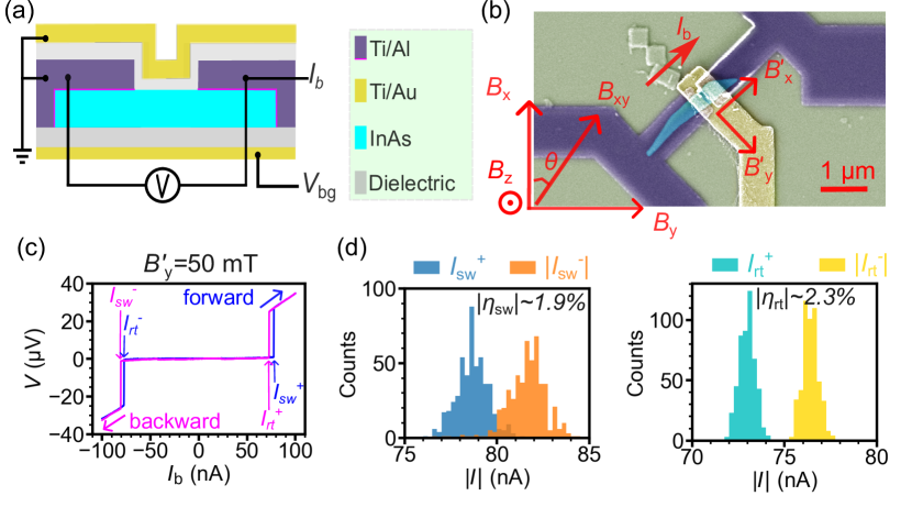
The Josephson junction devices were fabricated from InAs nanosheets grown via molecular beam epitaxy (see Ref. 39 for details of the InAs nanosheets growth). The nanosheets were mechanically transferred onto pre-patterned local back gates with 15-nm-thick grown by atomic layer deposition (ALD) as a dielectric layer. The contact areas were defined by electron-beam lithography. Then, the samples were etched in a diluted solution to remove the native oxide layer, followed by a deposition of 5 nm Ti using electron-beam evaporation and 50 nm Al using thermal evaporation. Top gates were fabricated with a deposition of 5/15 nm Ti/Au after growing 15 nm with ALD. Figure 1a displays a schematic side view of the fabricated devices together with the measurement circuit. Figure 1b shows a false-colored scanning electron microscope (SEM) image of device A. For this device, the InAs nanosheet at the junction is approximately wide, with a gap of between the superconducting electrodes. Electrical transport measurements were performed on the device in a dilution refrigerator equipped with a vector magnet. In Figure 1b, the axes , , and indicate the coordinate of the vector magnet, while the axes and are a new coordinate with respect to the current direction . is an in-plane magnetic field with an angle with respect to . Two comparable devices (A and B) were studied, with all the results presented in the main article derived from device A, while the results from device B are provided in the Supporting Information (Additional Data Section). Top-gates were grounded throughout this work.
Figure 1c presents an example of the measured Josephson diode effect (JDE) at . The voltage across the junction of the hybrid device is measured in a four-terminal measurement circuit setup while a bias current is applied (see Figure 1a). The blue and pink curves represent the results for forward and backward current sweeping directions, respectively. A characteristic hysteretic behavior is evident in both forward and backward sweeps, i.e. and , which can be attributed to phase instability in the junction and/or heating effects.40, 41, 42, 43, 43 Aside from the hysteresis, JDE is observed as a finite difference between the absolute values of forward sweep switching current and backward sweep switching current |. Additionally, there exists a finite difference between the absolute values of the retrapping current of forward and backward sweep and , further confirming the presence of JDE.30, 29 Since the switching current in a Josephson junction is typically stochastic44, 30, 29, repeated measurements are beneficial for an accurate analysis of JDE. Figure 1d presents histograms of switching current distribution, obtained from N=500 forward sweeping events followed by N=500 backward sweeping events under the same magnetic field conditions as in Figure 1c. In the left histogram, there is a clear separation between and bunches. An averaged forward switching current, as well as backward switching current, is calculated from the distributions. The JDE efficiency of switching current is then calculated by using the averaged values: =(-||)/(+|). Similarly, the histograms for the retrapping current are shown in the right panel of Figure 1d, and the diode efficiency of retrapping current is calculated as ). Here, we obtain and . These values are consistent with previous reports of JDE in Josephson junctions based on low-dimensional semiconductors with strong SOI.19, 20, 30 Note that the variation of switching current is larger than that of retrapping current, potentially due to suppression of the stochastic behavior of retrapping current by heating effects.30, 29 The data presented for , , and in the rest of this article are averaged over repeated measurements similar as done in Figure 1d unless stated otherwise.
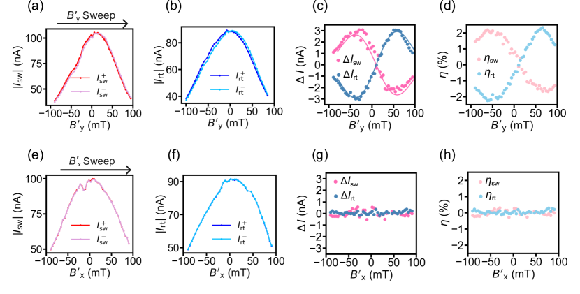
Figure 2 shows the magnetic field dependence of JDE along two different directions. Here, and represents configurations where the in-plane magnetic field is perpendicular and parallel to the direction of , respectively (as seen in Figure 1b). Figure 2a presents the absolute values of and as a function of and Figure 2b shows the results for retrapping currents. In the two figures, both switching and retrapping currents decrease with increasing magnetic field caused by the suppression of induced superconductivity. Meanwhile, a nonzero difference between and (as well as between and ) can be recognized. The difference between switching currents and the difference between retrapping currents are plotted as solid dots in Figure 2c. In the figure, both (in pink) and (in blue) show antisymmetric behaviors relative to , i.e. and , with maximum and minimum values at . Figure 2d exhibits diode efficiency and as a function of , and the maximum efficiency exceeds for both and . In Figure 2a-2d, is swept from negative to positive, and similar results can be observed when the field sweep direction is reversed (i.e., from positive to negative, see Figure S4 in the Supporting Information). When the in-plane magnetic field is parallel to bias current, suppression of switching current and retrapping current could also be observed, as shown in Figure 2e and 2f. However, almost no signal of JDE is observed, as can be seen in Figure 2g and 2h. JDE measurements as in Figure 2 have been done on device B, and similar results are observed (see details in Figure S6 in the Supporting Information). In Figure 2, both and are nearly zero throughout the measurement range of . This excludes a possible explanation that or has a residual out-of-plane component leading to JDE.24 Based on our previous work, the Rashba-type SOI is dominant in InAs nanosheets, with its direction perpendicular to the bias current within the nanosheet plane.45 Hereafter, the results are analyzed in the context of finite momentum pairing induced by Rashba SOI and magnetic field. When a magnetic field is applied along SOI field (i.e., in our device), a momentum shift is acquired for Cooper pairs when crossing a JJ.10, 46 Consequently, a phase shift is present for supercurrent across the junction,47, 32 where is the gap length between the two superconducting leads. At small magnetic fields, is linear with , so , where is a parameter dependent on the junction’s geometry and material properties. The finite phase shift together with high-quality semiconductor-superconductor interface (see Figures S2 and S3 in the Supporting Information) would ultimately resulting in JDE.16, 10, 15, 34, 20 Following Ref. 15 , the switching current difference is governed by the equation: , where is the applied magnetic field and is the critical magnetic field of the JJ.10, 15, 20 In Figure 2c, and are fitted with the above formula, where is taken (see Figure S1 in the Supporting Information), and the fitting curves are displayed as pink and blue solid lines. The well agreement between the data and the fitting curves confirms that finite momentum pairing is likely the origin of the JDE appearing in our devices.
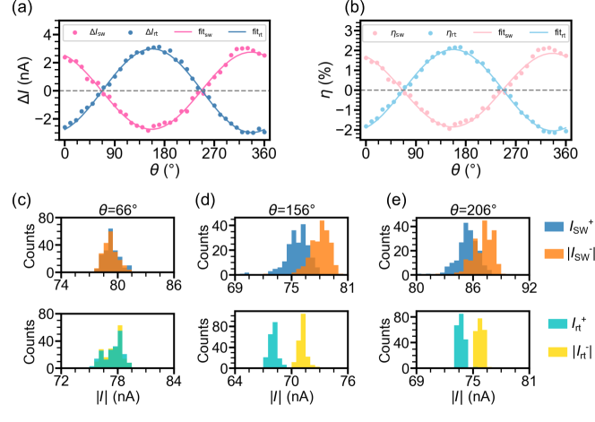
Figure 3 displays the dependence of the JDE on the direction of in-plane magnetic field with a fixed amplitude . In Figure 3a, (pink dots) and (blue dots) are plotted as a function of , where represents the angle between and (see Figure 1b). Figure 3b shows the dependence of diode efficiency (pink dots) and (blue dots) on angle . In the two figures, the gray dashed line indicates the position where or , and solid lines are sinusoidal fits. From the sinusoidal fits, the angles corresponding to maximum and minimum JDE are approximately and , respectively. Note that at , is aligned with . Figures 3c-3e show histogram distributions from N=200 measurements for switching current (upper panels) and retrapping current (lower panels) at equals to (), () and (in between), respectively. These distributions reveal a clear trend of a more pronounced JDE as rotates from being parallel to being perpendicular to . As discussed in the last paragraph, finite momentum paring takes place when magnetic field and SOI field are in parallel (), and a finite phase shift emerges for Cooper pairs transporting along a perpendicular direction (i.e., or ).46 When is rotated from being parallel to being perpendicular to , the component of the field along increases, therefore enhancing the finite momentum pairing and JDE. This is validated by the sinusoidal shape of the results in Figures 3 a and 3 b. In a nutshell, the angle-dependence of the JDE shows well agreement with the mechanism of finite momentum pairing induced by Rashba SOI and magnetic field.
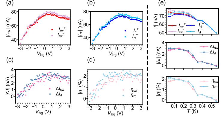
In principle, finite momentum pairing in superconductor-semiconductor hybrid JJs can originate from screening effect or interaction between Zeeman effect and SOI.10, 9, 15, 25 Studying the dependence of JDE on gate voltage is helpful for tracking its microscopic origin.10, 9 Figure 4a shows switching current, and ||, as a function of back gate voltage . The supercurrent keeps increasing for from -3 to and drops slightly from 0.5 to . Similar behaviors are observed for retrapping current as shown in Figure 4b. The supercurrent rise in the gate range of -3 to is caused by the increase of carrier density, which is supported by the decrease of the normal resistance of the device (see Figure S2 in the Supporting Information). The slight drop of the supercurrent in the range of 0.5 to is likely due to gate-controlled induced superconductivity.48 Figure 4c and 4d display the gate dependence of the supercurrent difference ( and ) and the diode efficiency ( and ). JDE shows a monotonic suppression as decreases from 0.5 to . Notably, at , the JDE completely vanishes, with both and . In contrast, a significant amount of supercurrent is still conserved at as seen in Figure 4a. Such a gate-controlled JDE indicates that screening effect is not the origin of the non-reciprocal supercurrent in this work.9, 10 The vanish of the JDE in Figure 4c and 4d can arise from a lowered superconductor-semiconductor interface transparency or a suppressed finite momentum pairing. The former reason can be excluded as the interface transparency does not drop with a more negative gate voltage, but rather increases (see Figure S2 in the Supporting Information). According to our previous study, the Rashba SOI in the InAs nanosheets can be quenched at particular gate voltages as a result of suppressed vertical electric field.45 Therefore, the vanish of the JED tends to be caused by the suppression of finite momentum pairing via a gate-controlled SOI. In Figure 4c and 4d, JDE exhibits a near-saturation or a slight-drop behavior as increases 0.5 to , likely due to a competing effect among tunable parameters such as chemical potential, SOI strength, and interface transparency. Figure 4e shows temperature dependence of the JDE. As the temperature increases, both the switching and retrapping currents exhibit a nearly monotonic decrease, which is attributed to the closing of the superconducting gap. Around , the remaining supercurrent is approximately 50 nA. As a comparison, both the supercurrent difference ( and ) and the diode efficiency ( and ) drop to zero as increases to . The complete suppression of the JDE can be attributed to a reduction in the transparency of the semiconductor-superconductor interface.19
In conclusion, we have demonstrated the existence of intrinsic Josephson diode effect (JDE) in planar Josephson junctions made from InAs nanosheets with superconducting aluminum contacts. The JDE is likely driven by finite-momentum pairing, which arises from the interplay between Rashba spin-orbit interaction (SOI) and Zeeman splitting under an in-plane magnetic field. In experiments, we see a strong dependence of the JDE on magnetic field orientation and the JDE is maximized when the magnetic field is aligned with the expected spin-orbit field. Importantly, we observe that the JDE is highly tunable via electrostatic gating with a complete suppression at specific gate voltages, indicating the critical role of Rashba SOI in enabling the non-reciprocal superconducting current. Our findings contribute to the growing body of research demonstrating that JDE is not only a fundamental phenomenon to explore novel physics of nonreciprocal superconductivity but also holds promise for applications in superconducting electronics, spintronics, and quantum information technology. The ability to continuously control JDE through gate voltage offers exciting prospects for developing low-power, non-dissipative components for superconducting circuits, including rectifiers, memory elements, and logic devices.
3 Author contributions
H.Q.X conceived and supervised the project. S.Y., H.S., H.G and X.W. fabricated the devices. D.P. and J.Z. grew the InAs nanosheets. S.Y., J.Y.W. and Y.L. performed the transport measurements. S.Y., J.Y.W. and H.Q.X. analyzed the measurement data. S.Y., J.Y.W. and H.Q.X. wrote the manuscript with inputs from all the authors.
4 Supporting Information
The Supporting Information includes: details of device fabrication and additional transport experiment data (PDF).
The authors would like to thank Dr. Po Zhang for his assistance with the measurement codes. This work is supported by the National Natural Science Foundation of China (Grant Nos. 92165208, 11874071, 92365103, 12374480, 12374459, 61974138 and 92065106). D.P. acknowledges the support from Youth Innovation Promotion Association, Chinese Academy of Sciences (Nos. 2017156 and Y2021043).
5 Data analysis and data availability
The raw data and the analysis files are available upon request.
6 Conflict of interests
The authors declare no conflict of interests.
References
- Linder and Robinson 2015 Linder, J.; Robinson, J. W. Superconducting spintronics. Nature.Phys. 2015, 11, 307–315
- Braginski 2019 Braginski, A. I. Superconductor electronics: Status and outlook. J. Supercond. Nov. Magn. 2019, 32, 23–44
- Wendin 2017 Wendin, G. Quantum information processing with superconducting circuits: a review. Rep.Prog. Phys. 2017, 80, 106001
- Nadeem et al. 2023 Nadeem, M.; Fuhrer, M. S.; Wang, X. The superconducting diode effect. Nat. Rev. Phys. 2023, 5, 558–577
- Legg et al. 2023 Legg, H. F.; Laubscher, K.; Loss, D.; Klinovaja, J. Parity-protected superconducting diode effect in topological Josephson junctions. Phys. Rev. B 2023, 108, 214520
- Ando et al. 2020 Ando, F.; Miyasaka, Y.; Li, T.; Ishizuka, J.; Arakawa, T.; Shiota, Y.; Moriyama, T.; Yanase, Y.; Ono, T. Observation of superconducting diode effect. Nature 2020, 584, 373–376
- He et al. 2022 He, J. J.; Tanaka, Y.; Nagaosa, N. A phenomenological theory of superconductor diodes. N. J. .Phys. 2022, 24, 053014
- Daido et al. 2022 Daido, A.; Ikeda, Y.; Yanase, Y. Intrinsic superconducting diode effect. Phys. Rev. Lett. 2022, 128, 037001
- Yuan and Fu 2022 Yuan, N. F.; Fu, L. Supercurrent diode effect and finite-momentum superconductors. Proc. Natl Acad. Sci. USA 2022, 119, e2119548119
- Davydova et al. 2022 Davydova, M.; Prembabu, S.; Fu, L. Universal Josephson diode effect. Sci. Adv. 2022, 8, eabo0309
- Legg et al. 2022 Legg, H. F.; Loss, D.; Klinovaja, J. Superconducting diode effect due to magnetochiral anisotropy in topological insulators and Rashba nanowires. Phys. Rev. B 2022, 106, 104501
- Ilić and Bergeret 2022 Ilić, S.; Bergeret, F. S. Theory of the supercurrent diode effect in Rashba superconductors with arbitrary disorder. Phys. Rev. Lett. 2022, 128, 177001
- Souto et al. 2022 Souto, R. S.; Leijnse, M.; Schrade, C. Josephson diode effect in supercurrent interferometers. Phys. Rev. Lett. 2022, 129, 267702
- Ciaccia et al. 2023 Ciaccia, C.; Haller, R.; Drachmann, A. C. C.; Lindemann, T.; Manfra, M. J.; Schrade, C.; Schönenberger, C. Gate-tunable Josephson diode in proximitized InAs supercurrent interferometers. Phys. Rev. Res. 2023, 5, 033131
- Pal et al. 2022 Pal, B. et al. Josephson diode effect from Cooper pair momentum in a topological semimetal. Nat. Phys. 2022, 18, 1228–1233
- Baumgartner et al. 2022 Baumgartner, C.; Fuchs, L.; Costa, A.; Reinhardt, S.; Gronin, S.; Gardner, G. C.; Lindemann, T.; Manfra, M. J.; Faria Junior, P. E.; Kochan, D.; others Supercurrent rectification and magnetochiral effects in symmetric Josephson junctions. Nat. Nanotechnol. 2022, 17, 39–44
- Bauriedl et al. 2022 Bauriedl, L.; Bäuml, C.; Fuchs, L.; Baumgartner, C.; Paulik, N.; Bauer, J. M.; Lin, K.-Q.; Lupton, J. M.; Taniguchi, T.; Watanabe, K.; Strunk, C. Supercurrent diode effect and magnetochiral anisotropy in few-layer NbSe2. Nat. Commun. 2022, 13, 4266
- Lin et al. 2022 Lin, J.-X.; Siriviboon, P.; Scammell, H. D.; Liu, S.; Rhodes, D.; Watanabe, K.; Taniguchi, T.; Hone, J.; Scheurer, M. S.; Li, J. Zero-field superconducting diode effect in small-twist-angle trilayer graphene. Nat. Phys. 2022, 18, 1221–1227
- Turini et al. 2022 Turini, B.; Salimian, S.; Carrega, M.; Iorio, A.; Strambini, E.; Giazotto, F.; Zannier, V.; Sorba, L.; Heun, S. Josephson diode effect in high-mobility InSb nanoflags. Nano Lett. 2022, 22, 8502–8508
- Mazur et al. 2024 Mazur, G.; van Loo, N.; van Driel, D.; Wang, J.-Y.; Badawy, G.; Gazibegovic, S.; Bakkers, E.; Kouwenhoven, L. Gate-tunable Josephson diode. Phys. Rev. Appl. 2024, 22, 054034
- Golod and Krasnov 2022 Golod, T.; Krasnov, V. M. Demonstration of a superconducting diode-with-memory, operational at zero magnetic field with switchable nonreciprocity. Nat. Commun. 2022, 13, 3658
- Gutfreund et al. 2023 Gutfreund, A.; Matsuki, H.; Plastovets, V.; Noah, A.; Gorzawski, L.; Fridman, N.; Yang, G.; Buzdin, A.; Millo, O.; Robinson, J. W. A.; Felner, I.; Uri, A.; Yochelis, S.; Hachmo, Y. Direct observation of a superconducting vortex diode. Nat. Commun. 2023, 14, 1630
- Ciaccia et al. 2023 Ciaccia, C.; Haller, R.; Drachmann, A. C.; Lindemann, T.; Manfra, M. J.; Schrade, C.; Schönenberger, C. Gate-tunable Josephson diode in proximitized InAs supercurrent interferometers. Phys. Rev. Res. 2023, 5, 033131
- Hou et al. 2023 Hou, Y.; Nichele, F.; Chi, H.; Lodesani, A.; Wu, Y.; Ritter, M. F.; Haxell, D. Z.; Davydova, M.; Ilić, S.; Glezakou-Elbert, O.; Fu, L.; Steele, G. A.; Lee, S. Ubiquitous superconducting diode effect in superconductor thin films. Phys. Rev. Lett. 2023, 131, 027001
- Banerjee et al. 2023 Banerjee, A.; Geier, M.; Rahman, M. A.; Thomas, C.; Wang, T.; Manfra, M. J.; Flensberg, K.; Marcus, C. M. Phase asymmetry of Andreev spectra from Cooper-pair momentum. Phys. Rev. Lett. 2023, 131, 196301
- Margineda et al. 2023 Margineda, D.; Crippa, A.; Strambini, E.; Fukaya, Y.; Mercaldo, M. T.; Cuoco, M.; Giazotto, F. Sign reversal diode effect in superconducting Dayem nanobridges. Commun. Phys. 2023, 6, 343
- Costa et al. 2023 Costa, A.; Baumgartner, C.; Reinhardt, S.; Berger, J.; Gronin, S.; Gardner, G. C.; Lindemann, T.; Manfra, M. J.; Fabian, J.; Kochan, D.; Paradiso, N.; Strunk, C. Sign reversal of the Josephson inductance magnetochiral anisotropy and 0–-like transitions in supercurrent diodes. Nat. Nanotechnol. 2023, 18, 1266–1272
- Valentini et al. 2024 Valentini, M. et al. Parity-conserving Cooper-pair transport and ideal superconducting diode in planar germanium. Nat. Commun. 2024, 15, 169
- Su et al. 2024 Su, H.; Wang, J.-Y.; Gao, H.; Luo, Y.; Yan, S.; Wu, X.; Li, G.; Shen, J.; Lu, L.; Pan, D.; Jianhua, Z.; Zhang, P.; Xu, H. Q. Microwave-assisted unidirectional superconductivity in Al-InAs nanowire-Al junctions under magnetic fields. Phys. Rev. Lett. 2024, 133, 087001
- Lotfizadeh et al. 2024 Lotfizadeh, N.; Schiela, W. F.; Pekerten, B.; Yu, P.; Elfeky, B. H.; Strickland, W. M.; Matos-Abiague, A.; Shabani, J. Superconducting diode effect sign change in epitaxial Al-InAs Josephson junctions. Commun. Phys. 2024, 7, 120
- Edelstein 1996 Edelstein, V. M. The Ginzburg-Landau equation for superconductors of polar symmetry. J. Phys. Condens. Matter 1996, 8, 339
- Szombati et al. 2016 Szombati, D.; Nadj-Perge, S.; Car, D.; Plissard, S.; Bakkers, E.; Kouwenhoven, L. Josephson 0-junction in nanowire quantum dots. Nat. Phys. 2016, 12, 568–572
- Ke et al. 2019 Ke, C.-T.; Moehle, M. M.; de Vries, F.; Thomas, C.; Metti, S.; Guinn, C. R.; Kallaher, R.; Lodari, M.; Scappucci, G.; Wang, T.; Diaz, R. E.; Gardner, G. C.; Manfra, M. J.; Goswami, S. Ballistic superconductivity and tunable –junctions in InSb quantum wells. Nat. Commun. 2019, 10, 3764
- Zhang et al. 2022 Zhang, B.; Li, Z.; Aguilar, V.; Zhang, P.; Pendharkar, M.; Dempsey, C.; Lee, J. S.; Harrington, S. D.; Tan, S.; Meyer, J. S.; Palmstrøm, C. J.; Shabani, J. Evidence of 0-Josephson junction from skewed diffraction patterns in Sn-InSb nanowires. arXiv preprint arXiv:2212.00199 2022,
- Costa et al. 2023 Costa, A.; Fabian, J.; Kochan, D. Microscopic study of the Josephson supercurrent diode effect in Josephson junctions based on two-dimensional electron gas. Phys. Rev. B 2023, 108, 054522
- Pientka et al. 2017 Pientka, F.; Keselman, A.; Berg, E.; Yacoby, A.; Stern, A.; Halperin, B. I. Topological superconductivity in a planar Josephson junction. Phys. Rev. X 2017, 7, 021032
- Dartiailh et al. 2021 Dartiailh, M. C.; Mayer, W.; Yuan, J.; Wickramasinghe, K. S.; Matos-Abiague, A.; Žutić, I.; Shabani, J. Phase signature of topological transition in Josephson junctions. Phys. Rev. Lett. 2021, 126, 036802
- Shin et al. 2024 Shin, J.; Han, J.-H.; Rathore, A.; Lee, J. S.; Shim, S.-B.; Cha, J.; Park, S.; Suh, J. Electric Control of Polarity in Spin-Orbit Josephson Diode. arXiv preprint arXiv:2409.17820 2024,
- Pan et al. 2019 Pan, D.; Wang, J.-Y.; Zhang, W.; Zhu, L.; Su, X.; Fan, F.; Fu, Y.; Huang, S.; Wei, D.; Zhang, A. Y., Lijun Manling Sui; Xu, H. Q. Dimension engineering of high-quality InAs nanostructures on a wafer scale. Nano Lett. 2019, 19, 1632–1642
- Tinkham 2004 Tinkham, M. Introduction to superconductivity; Courier Corporation, 2004
- Tinkham et al. 2003 Tinkham, M.; Free, J.; Lau, C.; Markovic, N. Hysteretic I- V curves of superconducting nanowires. Phys. Rev. B 2003, 68, 134515
- Courtois et al. 2008 Courtois, H.; Meschke, M.; Peltonen, J.; Pekola, J. P. Origin of hysteresis in a proximity Josephson junction. Phys. Rev. Lett. 2008, 101, 067002
- Yan et al. 2023 Yan, S.; Su, H.; Pan, D.; Li, W.; Lyu, Z.; Chen, M.; Wu, X.; Lu, L.; Zhao, J.; Wang, J.-Y.; Xu, H. Q. Supercurrent, multiple Andreev reflections and Shapiro steps in InAs nanosheet Josephson junctions. Nano Lett. 2023, 23, 6497–6503
- Doh et al. 2005 Doh, Y.-J.; van Dam, J. A.; Roest, A. L.; Bakkers, E. P.; Kouwenhoven, L. P.; De Franceschi, S. Tunable supercurrent through semiconductor nanowires. Science 2005, 309, 272–275
- Fan et al. 2022 Fan, F.; Chen, Y.; Pan, D.; Zhao, J.; Xu, H. Q. Electrically tunable spin–orbit interaction in an InAs nanosheet. Nanoscale Advances 2022, 4, 2642–2648
- Zhang et al. 2022 Zhang, Y.; Gu, Y.; Li, P.; Hu, J.; Jiang, K. General theory of Josephson diodes. Phys. Rev. X 2022, 12, 041013
- Yokoyama et al. 2014 Yokoyama, T.; Eto, M.; Nazarov, Y. V. Anomalous Josephson effect induced by spin-orbit interaction and Zeeman effect in semiconductor nanowires. Phys. Rev. B 2014, 89, 195407
- van Loo et al. 2023 van Loo, N.; Mazur, G. P.; Dvir, T.; Wang, G.; Dekker, R. C.; Wang, J.-Y.; Lemang, M.; Sfiligoj, C.; Bordin, A.; van Driel, D.; Badawy, G.; Gazibegovic, S.; P. A. M. Bakkers, E.; P. Kouwenhoven, L. Electrostatic control of the proximity effect in the bulk of semiconductor-superconductor hybrids. Nat. Commun. 2023, 14, 3325