Resolving Contradictory Estimates of Band Gaps of Bulk PdSe2: A Wannier-Localized Optimally-Tuned Screened Range-Separated Hybrid Density Functional Theory Study
Abstract
Palladium diselenide (PdSe2)—a layered van der Waals material—is attracting significant attention for optoelectronics due to the wide tunability of its band gap from the infrared through the visible range as a function of the number of layers. However, there continues to be disagreement over the precise nature and value of the optical band gap of bulk PdSe2, owing to the rather small value of this gap that complicates experimental measurements and their interpretation. Here, we design and employ a Wannier-localized optimally-tuned screened range-separated hybrid (WOT-SRSH) functional to investigate the electronic bandstructures and optical absorption spectra of bulk and monolayer PdSe2. In particular, we account carefully for the finite exciton center-of-mass momentum within a time-dependent WOT-SRSH framework to calculate the indirect optical gap and absorption onset accurately. Our results agree well with the best available photoconductivity measurements, as well as with state-of-the-art many-body perturbation theory calculations, confirming that bulk PdSe2 has an optical gap in the mid-infrared (upper-bound of 0.44 eV). More generally, this work further bolsters the utility of the WOT-SRSH approach for predictive modeling of layered semiconductors.
Layered van der Waals (vdW) materials have attracted significant attention over the last two decades, both in fundamental and applied research, due to their wide range of electronic, magnetic, optical, and structural behaviors.Geim and Grigorieva (2013); Novoselov et al. (2016); Ajayan, Kim, and Banerjee (2016); Duong, Yun, and Lee (2017) In particular, the ability of these vdW materials to be thinned down to the single- or few-layer limit has enabled wide-ranging discoveries in low-dimensional (2D) physics with the promise of novel applications in nanoscale optoelectronics.Xia et al. (2014); Zhou et al. (2018); Zhang et al. (2016)
Palladium diselenide (PdSe2), a layered noble transition-metal dichalcogenide, is a particularly interesting member of the vdW family whose optical band gap is widely tunable over an approximate range of 0.5-1.5 eV when going from the bulk to the monolayer.Wei et al. (2022); Oyedele et al. (2017); Zhang et al. (2019) The small bulk band gap, accompanied by its wide tunability with sample thickness, makes PdSe2 particularly attractive for optoelectronics in the mid- to near-infrared (IR),Long et al. (2019); Wang et al. (2022); Sefidmooye Azar et al. (2021) an application domain that has been explored more thoroughly with black phosphorus, which is unfortunately prone to degradation under normal ambient conditions.Island et al. (2015); Artel et al. (2017); Debnath, Park, and Song (2018) Indeed, recent work has demonstrated highly-responsive PdSe2 IR photodetectors,Zhang et al. (2019); Long et al. (2019); Wang et al. (2022); Sefidmooye Azar et al. (2021) as well as broadband devices,Dong et al. (2021); Zeng et al. (2019); Wu et al. (2019); Chen et al. (2021) that are stable during fabrication and operation. Few-layer PdSe2 is also known to exhibit unusual switching in its anisotropic linear dichroism response,Yu et al. (2020) providing an extra degree of control for optical switching, communication and polarization-dependent detection.Liang et al. (2022); Long et al. (2019) Beyond optical response, ultra-thin field-effect transistors based on few-layer PdSe2 have been shown to exhibit ambipolar behavior accompanied by high carrier mobilities.Chow et al. (2017) These examples, among others, highlight the promise of PdSe2 and motivate continuing interest in this material.
Notwithstanding numerous investigations of PdSe2, a definitive determination of its bulk band gap remains elusive. An ARPES studyCattelan et al. (2021) showed that bulk PdSe2 is semiconducting, although the fundamental gap was not determined in that work. Measurements of the optical band gap of bulk PdSe2 range from 0.0-0.5eVOyedele et al. (2017); Zhang et al. (2019); Zeng et al. (2019); Hulliger (1965) introducing uncertainty even in the qualitative behavior of this material (semi-metallic vs. semiconducting). Nishiyama et al. Nishiyama et al. (2022a) suggest that older absorption measurementsOyedele et al. (2017); Zeng et al. (2019) are less reliable due to the large uncertainty introduced when determining optical gaps from Tauc plots. Instead, they estimated an indirect band gap of 0.5 eV (at 40 K) from photocurrent measurements that is consistent with photoresponse measurements by Zhang et al.Zhang et al. (2019) On the computational front, density functional theory (DFT) calculations with semilocal functionals suggest the bulk is (nearly) metallic, with gaps ranging from 0-0.03 eV Oyedele et al. (2017); Sun et al. (2015); Kim and Choi (2021) in clear disagreement with experiments. A recent many-body perturbation theory (MBPT) studyKim and Choi (2021) based on the “single-shot” G0W0 approximation,Hybertsen and Louie (1986) starting from the semilocal PBE functional, Perdew, Burke, and Ernzerhof (1996) reported an indirect fundamental gap of 0.45 eV. We are unaware of any state-of-the-art calculations of the optical gap of bulk PdSe2, that typically employ the Bethe-Salpeter equation (BSE)Salpeter and Bethe (1951) to obtain neutral excitation energies starting from GW quasiparticle energies. Also, such GW-BSE calculations are usually performed only for direct optical transitions (zero-momentum excitons) and there are but a few examples of GW-BSE calculations for indirect transitions (finite-momentum excitons) in layered materials,Deilmann and Thygesen (2019); Mei et al. (2022); Lettmann and Rohlfing (2021) a key requirement for determining the absorption onset of bulk PdSe2 accurately. In contrast to bulk PdSe2, the situation for the monolayer is clearer, with experiment and theory agreeing, at least, on its semiconducting nature. Experimental measurements of the optical band gap range between 1.25-1.37eV, Oyedele et al. (2017); Zhang et al. (2019) DFT calculations with semilocal functionals yield band gaps between 1.30-1.43 eV, Oyedele et al. (2017); Kuklin and Ågren (2019); Sun et al. (2015) and a GW0 studyKuklin and Ågren (2019) reported a quasiparticle gap of 2.55 eV.
While MBPT-based approaches are considered to be the state-of-the-art for first-principles electronic structure calculations, their accuracy comes at a high computational cost. Hence, there remains significant interest in developing less expensive yet equally accurate alternatives based on DFT and time-dependent DFT. A promising approach along these lines is based on tuned screened range-separated hybrid (SRSH) exchange-correlation functionals that have been shown to deliver quantitatively accurate predictions of fundamental and optical band gaps in the solid state.Wing et al. (2019); Ramasubramaniam, Wing, and Kronik (2019); Refaely-Abramson et al. (2015); Camarasa-Gómez et al. (2023) More recently, these SRSH functionals have been constructed via a self-consistent framework, based on enforcing an ionization-potential ansatz for maximally-localized Wannier functionsMostofi et al. (2008) to yield so-called Wannier-localized optimally-tuned SRSH (WOT-SRSH) functionals that are both quantitatively accurate in themselves and excellent starting points for subsequent MBPT calculations.Wing et al. (2021); Ohad et al. (2022); Gant et al. (2022); Ohad et al. (2023); Sagredo et al. (2024); Ohad et al. (2024) Very recently, we have extended the WOT-SRSH framework to bulk and monolayer phases of black phosphorus (BP), molybdenum disulfide (MoS2), and hexagonal boron nitride (hBN) and obtained accurate results.Camarasa-Gómez et al. (2024) Here, we apply the WOT-SRSH approach to model electronic bandstructures and absorption spectra of bulk and monolayer PdSe2. We show that the predictions are in good agreement with prior GW calculations,Kim and Choi (2021); Kuklin and Ågren (2019) as well as our own reference G0W0-BSE calculations. We also calculate optical absorption spectra—accounting for both direct () and finite-momentum () excitations—from which we find that the indirect optical gap of bulk PdSe2 is 0.44 eV, in good agreement with the above mentioned photocurrent measurements. Details of these calculations can be found in Sections S1 & S2 of the Supporting Materials.
The SRSH functional is constructed by partitioning the Coulomb kernel asLeininger et al. (1997); Yanai, Tew, and Handy (2004)
| (1) |
and treating the first and second terms of this equation using exact (Fock) exchange (XX) and semilocal (SL) DFT exchange, respectively; are parameters and is the error function. This procedure partitions the exchange interaction into short-range (SR) and long-range (LR) components with XX fractions of and , respectively, accompanied by their respective complementary SL fractions of and . The range-separation parameter, , governs the transition from SR to LR behavior. To enforce correct asymptotic screening of the Coulomb tail in the solid state, we set ,Refaely-Abramson et al. (2013) where is the average high-frequency macroscopic dielectric constant (neglecting anisotropy for now). The corresponding exchange potential, , is given by
| (2) |
For monolayers, we set , this being the exact asymptotic limit for screening in 2D;Cudazzo, Tokatly, and Rubio (2011); Andersen, Latini, and Thygesen (2015); Qiu, da Jornada, and Louie (2016) for bulk solids, is calculated ab initio as . To determine and , we enforce the ionization-potential (IP) ansatz for removal of one electron from the highest-energy occupied, maximally-localized Wannier function (). In particular, an optimal - pair must satisfy the relation
| (3) |
where is the total energy of the system with an electron removed from (calculated using constrained minimizationWing et al. (2021)), is the total energy of the neutral system, and is the expectation energy of with respect to the SRSH Hamiltonian. We direct the reader to Ref. Camarasa-Gómez et al., 2024 for details of this procedure specialized to layered materials.
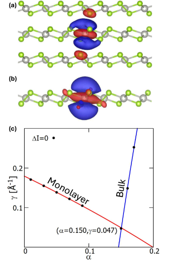
The outcome of the WOT procedure, along with plots of the Wannier functions employed for monolayer and bulk PdSe2, are displayed in Figure 1. As shown previously,Ramasubramaniam, Wing, and Kronik (2019); Camarasa-Gómez et al. (2024, 2023) two reference structures are needed to determine and uniquely for vdW layered materials, the monolayer and bulk phases being particularly convenient choices. While an infinite number of - pairs satisfy the IP ansatz (Eq. 3) for each phase, the intersection of the loci of these points for each phase results in a unique pair, and Å-1, that is simultaneously optimal for bulk and monolayer PdSe2 (see Section S3 for the full set of tuning calculations). With this optimally-tuned functional now at hand, we proceed to predictive calculations of electronic bandstructure and absorption spectra.
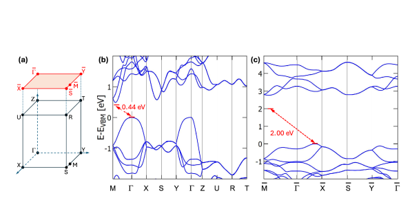
Figure 2 displays WOT-SRSH bandstructures for bulk and monolayer PdSe2, using well-converged -point meshes; direct and indirect band-gaps are reported in Table 1. Both bulk and monolayer PdSe2 are indirect gap semiconductors and our calculations further confirm that the conduction band minima lie in the interior of the Brillouin zone (along the / line) rather than along a high-symmetry direction.Kim and Choi (2021); Kuklin and Ågren (2019) The indirect bulk band gap is calculated to be 0.49 eV, which agrees well with Kim and Choi’s estimate of 0.45 eV.Kim and Choi (2021) The indirect gap for the monolayer is calculated to be 2.76 eV, which is slightly higher than Kim and Choi’s estimate of 2.37 eVKim and Choi (2021) but closer to Kuklin and Ågren’s estimate of 2.55 eV.Kuklin and Ågren (2019) For comparison, we also calculated quasiparticle band gaps independently by performing single-shot GW calculations with HSE06Heyd, Scuseria, and Ernzerhof (2003) wavefunctions as the starting point (Section S5). Using less dense -point meshes—necessitated by the high computational cost of full-frequency GW— for both the GW and WOT-SRSH calculations, the bulk band gap is estimated to be 0.6 eV and 0.57 eV, respectively. As seen in our prior GW calculations,Ramasubramaniam, Wing, and Kronik (2019); Camarasa-Gómez et al. (2023) converging the calculation with respect to the -point mesh is expected to reduce the GW gap and bring it closer to the the converged WOT-SRSH estimate. Similarly, for the monolayer, a comparison of GW and WOT-SRSH calculations using -point meshes reveals very similar indirect gaps of 2.73 eV and 2.76 eV, respectively. It is well known that GW calculations are sensitive to the choice of starting point; the WOT-SRSH approach, on the other hand is not only internally self-consistent but has also been shown to be a good starting point for single-shot GW calculations.Gant et al. (2022); Camarasa-Gómez et al. (2024) This fact, bolstered by the good agreement between our WOT-SRSH and single-shot GW (over HSE) results, leads us to believe that our calculated fundamental band gaps are reliable. While we are unaware of any direct measurements of the fundamental band gap of bulk PdSe2, electrical transport gaps range from 0.3 eV (18-191 nm thick flakes) Nishiyama et al. (2022b) to 0.57 eV (6.8 nm thick flake),Zhang et al. (2019) but these results could be affected by the presence of trap states as well inherent uncertainties in device modeling parameters (see Section S4 for a more complete comparison of calculated and measured band gaps). For completeness, we note that inclusion of spin-orbit coupling alters our estimates of both bulk and monolayer WOT-SRSH band gaps by 10 meV with insignificant differences in the overall band structure (Section S5).
| Phase | [Å-1] | -grid | E [eV] | E [eV] | E [eV] | E [eV] | ||
|---|---|---|---|---|---|---|---|---|
| Bulk | 0.150 | 0.047 | 12.136 | 0.49 (0.45 Kim and Choi (2021)) | 1.27 (1.10 Kim and Choi (2021)) | 0.44 | 1.11 | |
| Monolayer | 0.150 | 0.047 | 1 | 2.76 (2.37,Kim and Choi (2021) 2.53 Kuklin and Ågren (2019)) | 2.98 (2.54,Kim and Choi (2021) 2.62Kuklin and Ågren (2019) ) | 2.00 | 2.20 (2.01Kuklin and Ågren (2019)) |
To make a clear connection with optical measurements, we calculated the optical response of bulk and monolayer PdSe2 using linear-response, time-dependent DFT calculations that employ the WOT-SRSH functional (TD-SRSH). We have used this approach successfully to model the absorption spectra and to extract exciton binding energies for several 2D materials, albeit only for vertical transitions, i.e., when excitons couple to incoming photons with vanishingly small momenta (.Ramasubramaniam, Wing, and Kronik (2019); Camarasa-Gómez et al. (2023, 2024) However, an exciton can indeed carry a finite center-of-mass momentum, , and this is central to understanding exciton dispersion and excitonic bandstructures of materials;Deilmann and Thygesen (2019); Gatti and Sottile (2013); Sander, Maggio, and Kresse (2015); Qiu, Cao, and Louie (2015); Noffsinger et al. (2012) we refer the reader to the cited literature for details and focus on the practical aspects of this problem for now. Specifically, our interest here is to employ finite-momentum calculations, within the framework of TD-SRSH, to calculate the indirect optical band gaps (Fig. 2) and thereby resolve contradictory reports in the literature, in particular, for bulk PdSe2. To this end, we assign finite exciton center-of-mass momenta and to the bulk and monolayer, respectively, and calculate the excitation spectrum;111The center-of-mass momentum vector, , is denoted here as a multiple of the reciprocal lattice vectors. The band-edge extrema obtained from Wannier interpolation (Fig. 2) do not necessarily coincide with sampling points in the regular -point mesh used for self-consistent calculations. As VASP requires to be expressible as a difference between two -points, not allowing for interpolation to irregular points, we pick -points that are as close as possible to the valence band maximum and the conduction band minimum. Thus, our estimates for optical gaps are upper bounds. The resulting overestimate of the optical gap can be approximated by the difference of the electronic band gap between the two sampled points and the true indirect fundamental band gap, and we estimate this error to be 13.5 meV for the bulk and 5.3 meV for the monolayer. The error can be reduced with denser -point grids. we do not include electron-phonon coupling termsNoffsinger et al. (2012) in the optical matrix elements for now, deferring this to future work. Figure 3(a) displays the absorption spectra for transitions with ; spectra for transitions are provided in Section S6. Resolving the absorption spectra more clearly (Fig. 3(a), inset), we find that the lowest indirect optical transition () for bulk PdSe2 is at 0.44 eV, 11footnotemark: 1 approximately, 0.05 eV below the fundamental indirect gap. The lowest direct optical transition () is at much higher energy (1.11 eV) and not directly relevant to the absorption onset, underscoring the need for finite-momentum calculations. To reinforce the validity of the TD-SRSH results, we also calculated these optical transitions using the GW-BSE approach (using a coarser -grid, as noted above). The two sets of calculations, based on entirely different methodologies, are in good agreement (Sections S6 & S7), yielding indirect optical gaps of 0.58 eV (GW-BSE) and 0.47 eV (TD-SRSH). For the monolayer, we find TD-SRSH optical gaps of 2.00 eV (indirect) and 2.20 eV (direct), which implies that excitons are strongly bound (0.75 eV binding energy) in this 2D system.Ramasubramaniam (2012) Our TD-SRSH estimates for direct optical gaps are slightly higher but still in good agreement with other reports (2.01 eV; GW-BSE Kuklin and Ågren (2019)); both direct and indirect TD-SRSH gaps are also in good agreement (to within 100 meV) with our own GW-BSE results (Section S7).
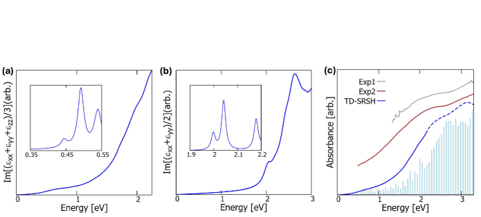
Our results now provide us with a clearer understanding of experimental reports, specifically, absorption measurements. As absorption data are typically presented as Tauc plots (absorbance vs. energy), from which band gaps are determined by linear extrapolation, we replot the bulk finite-momentum optical spectrum in this form in Figure 3, alongside data from two experiments.Oyedele et al. (2017); Zeng et al. (2019) We intentionally use a relatively large broadening of 0.1 eV to mimic the experimental data and emphasize that the tail below 0.44 eV is simply an artifact of this broadening.222Note that the actual absorption spectrum will contain contributions from multiple -vectors but we are only concerned with one momentum here to capture the absorption onset. Oyedele et al.’s absorption measurements (Exp1 in Fig. 3) stop at 1.3 eV, requiring linear extrapolation over a significant energy window to determine the absorption onset. Zeng et al.’s measurements extend to lower energies of 0.5 eV, but the nonlinearity in the data introduces errors in the extrapolation. These issues with the extrapolation procedure were also noted by Nishiyama et al.Nishiyama et al. (2022b) Conversely, band gaps inferred from photocurrent measurements (0.5 eV Zhang et al. (2019); Nishiyama et al. (2022a)) are in excellent agreement with our calculations and, collectively, theory and experiment confirm that bulk PdSe2 (in its pristine state) is indeed a small-gap semiconductor with absorption onset in the mid-infrared.
In conclusion, we have designed and employed a Wannier-optimally tuned screened range-separated (WOT-SRSH) hybrid functional to model the optoelectronic properties of bulk and monolayer PdSe2. This methodology is internally self-consistent and nonempirical, and delivers results that are in quantitative agreement with state-of-the-art GW-BSE calculations as well as the best available photocurrent measurements of bulk PdSe2. Our calculation of the finite-momentum excitonic spectrum is key to achieving this agreement with experiments, given that PdSe2 is an indirect gap material with a substantial difference between the direct and indirect gap. The straightforward resolution of conflicting reports in the literature provided here further confirms the potential of WOT-SRSH functionals for predictive modeling of semiconductors and insulators.
See the supplementary material for details of electronic-structure calculations; atomic positions and -point sampling; data from WOT tuning calculations; consolidated tables of electronic and optical band gaps from the literature and this work; and comparisons of GW/GW-BSE and WOT-SRSH/TD-SRSH results.
This work was supported by the National Science Foundation (NSF-BSF 2150562), the U.S.-Israel Binational Science Foundation (grant no. 2021721), and the Israel Science Foundation. M.C.-G. is grateful to the Azrieli Foundation for the award of an Azrieli International Postdoctoral Fellowship. L.K. acknowledges support from the Aryeh and Mintzi Katzman Professorial Chair, and the Helen and Martin Kimmel Award for Innovative Investigation.
Author Declarations
Conflict of Interest
The authors have no conflicts to disclose.
Author contributions
Fred Florio: Data curation (lead); Formal Analysis (equal); Methodology (equal); Visualization (lead); Writing – original draft (equal); María Camarasa-Gómez: Methodology (equal); Writing – review & editing (equal) Guy Ohad: Methodology (equal); Writing – review & editing (equal) Doron Naveh: Conceptualization (equal); Funding Acquisition (equal); Writing – review & editing (equal) Leeor Kronik: Funding Acquisition (equal); Writing – review & editing (equal) Ashwin Ramasubramaniam: Conceptualization (lead); Formal analysis (equal); Funding Acquisition (equal); Methodology (equal); Supervision (lead); Visualization (equal); Writing – original draft (equal)
Data Availability
The data that support the findings of this study are available from the corresponding authors upon reasonable request.
References
- Geim and Grigorieva (2013) A. Geim and I. Grigorieva, Nature 499, 419 (2013).
- Novoselov et al. (2016) K. S. Novoselov, A. Mishchenko, A. Carvalho, and A. H. Castro Neto, Science 353, aac9439 (2016).
- Ajayan, Kim, and Banerjee (2016) P. Ajayan, P. Kim, and K. Banerjee, Phys. Today 69, 38 (2016).
- Duong, Yun, and Lee (2017) D. L. Duong, S. J. Yun, and Y. H. Lee, ACS Nano 11, 11803 (2017).
- Xia et al. (2014) F. Xia, H. Wang, D. Xiao, M. Dubey, and A. Ramasubramaniam, Nature Photonics 8, 899 (2014).
- Zhou et al. (2018) X. Zhou, X. Hu, J. Yu, S. Liu, Z. Shu, Q. Zhang, H. Li, Y. Ma, H. Xu, and T. Zhai, Adv. Functional Mater. 28, 1706587 (2018).
- Zhang et al. (2016) W. Zhang, Q. Wang, Y. Chen, Z. Wang, and A. T. S. Wee, 2D Mater. 3, 022001 (2016).
- Wei et al. (2022) M. Wei, J. Lian, Y. Zhang, C. Wang, Y. Wang, and Z. Xu, npj 2D Mater. and Appl. 6, 1 (2022).
- Oyedele et al. (2017) A. D. Oyedele, S. Yang, L. Liang, A. A. Puretzky, K. Wang, J. Zhang, P. Yu, P. R. Pudasaini, A. W. Ghosh, Z. Liu, C. M. Rouleau, B. G. Sumpter, M. F. Chisholm, W. Zhou, P. D. Rack, D. B. Geohegan, and K. Xiao, J. of the Am. Chem. Soc. 139, 14090 (2017).
- Zhang et al. (2019) G. Zhang, M. Amani, A. Chaturvedi, C. Tan, J. Bullock, X. Song, H. Kim, D.-H. Lien, M. C. Scott, H. Zhang, and A. Javey, Appl. Phys. Lett. 114, 253102 (2019).
- Long et al. (2019) M. Long, Y. Wang, P. Wang, X. Zhou, H. Xia, C. Luo, S. Huang, G. Zhang, H. Yan, Z. Fan, X. Wu, X. Chen, W. Lu, and W. Hu, ACS Nano 13, 2511 (2019).
- Wang et al. (2022) Y. Wang, Y. Zhou, Z. Zhang, S. Xiao, J.-b. Xu, and H. K. Tsang, Appl. Phys. Lett. 120, 231102 (2022).
- Sefidmooye Azar et al. (2021) N. Sefidmooye Azar, J. Bullock, V. R. Shrestha, S. Balendhran, W. Yan, H. Kim, A. Javey, and K. B. Crozier, ACS Nano 15, 6573 (2021).
- Island et al. (2015) J. O. Island, G. A. Steele, H. S. van der Zant, and A. Castellanos-Gomez, 2D Mater. 2, 011002 (2015).
- Artel et al. (2017) V. Artel, Q. Guo, H. Cohen, Y. Liao, S. Yang, W. Zhang, J. Lin, X. Chen, G. Zhou, X. Liu, Y. Shi, Y. Wu, Z. Zhang, and X. Wang, npj 2D Materials and Applications 1, 6 (2017).
- Debnath, Park, and Song (2018) P. C. Debnath, K. Park, and Y.-W. Song, Small Methods 2, 1700315 (2018).
- Dong et al. (2021) Z. Dong, W. Yu, L. Zhang, H. Mu, L. Xie, J. Li, Y. Zhang, L. Huang, X. He, L. Wang, S. Lin, and K. Zhang, ACS Nano 15, 20403 (2021).
- Zeng et al. (2019) L.-H. Zeng, D. Wu, S.-H. Lin, C. Xie, H.-Y. Yuan, W. Lu, S. P. Lau, Y. Chai, L.-B. Luo, Z.-J. Li, and Y. H. Tsang, Adv. Functional Mater. 29, 1806878 (2019).
- Wu et al. (2019) D. Wu, J. Guo, J. Du, C. Xia, L. Zeng, Y. Tian, Z. Shi, Y. Tian, X. J. Li, Y. H. Tsang, and J. Jie, ACS Nano 13, 9907 (2019).
- Chen et al. (2021) X. Chen, J. Huang, C. Chen, M. Chen, G. Hu, H. Wang, and N. Dong, Adv. Opt. Mater. 10, 2101963 (2021).
- Yu et al. (2020) J. Yu, X. Kuang, Y. Gao, Y. Wang, K. Chen, Z. Ding, J. Liu, C. Cong, J. He, Z. Liu, and Y. Liu, Nano Lett. 20, 1172 (2020).
- Liang et al. (2022) Q. Liang, Z. Chen, Q. Zhang, and A. T. S. Wee, Adv. Functional Mater. 32, 2203555 (2022).
- Chow et al. (2017) W. L. Chow, P. Yu, F. Liu, J. Hong, X. Wang, Q. Zeng, C.-H. Hsu, C. Zhu, J. Zhou, X. Wang, J. Xia, J. Yan, Y. Chen, D. Wu, T. Yu, Z. Shen, H. Lin, C. Jin, B. K. Tay, and Z. Liu, Adv. Mater. 29, 1602969 (2017).
- Cattelan et al. (2021) M. Cattelan, C. J. Sayers, D. Wolverson, and E. Carpene, 2D Mater. 8, 045036 (2021).
- Hulliger (1965) F. Hulliger, J. Phys. Chem. Solids 26, 639 (1965).
- Nishiyama et al. (2022a) W. Nishiyama, T. Nishimura, M. Nishioka, K. Ueno, S. Iwamoto, and K. Nagashio, Adv, Photon. Res. 3, 2200231 (2022a).
- Sun et al. (2015) J. Sun, H. Shi, T. Siegrist, and D. J. Singh, Appl. Phys. Lett. 107, 153902 (2015).
- Kim and Choi (2021) H.-G. Kim and H. J. Choi, Phys. Rev. B 103, 165419 (2021).
- Hybertsen and Louie (1986) M. S. Hybertsen and S. G. Louie, Phys. Rev. B 34, 5390 (1986).
- Perdew, Burke, and Ernzerhof (1996) J. P. Perdew, K. Burke, and M. Ernzerhof, Phys. Rev. Lett. 77, 3865 (1996).
- Salpeter and Bethe (1951) E. E. Salpeter and H. A. Bethe, Phys. Rev. 84, 1232 (1951).
- Deilmann and Thygesen (2019) T. Deilmann and K. S. Thygesen, 2D Mater. 6, 035003 (2019).
- Mei et al. (2022) H. Mei, Y. Xia, Y. Zhang, Y. Wu, Y. Chen, C. Ma, M. Kong, L. Peng, H. Zhu, and H. Zhang, Phys. Chem. Chem. Phys. 24, 9384 (2022).
- Lettmann and Rohlfing (2021) T. Lettmann and M. Rohlfing, Phys. Rev. B 104, 115427 (2021).
- Kuklin and Ågren (2019) A. V. Kuklin and H. Ågren, Phys. Rev. B 99, 245114 (2019).
- Wing et al. (2019) D. Wing, J. B. Haber, R. Noff, B. Barker, D. A. Egger, A. Ramasubramaniam, S. G. Louie, J. B. Neaton, and L. Kronik, Phys. Rev. Mater. 3, 064603 (2019).
- Ramasubramaniam, Wing, and Kronik (2019) A. Ramasubramaniam, D. Wing, and L. Kronik, Phys. Rev. Mater. 3, 084007 (2019).
- Refaely-Abramson et al. (2015) S. Refaely-Abramson, M. Jain, S. Sharifzadeh, J. B. Neaton, and L. Kronik, Phys. Rev. B 92, 081204 (2015).
- Camarasa-Gómez et al. (2023) M. Camarasa-Gómez, A. Ramasubramaniam, J. B. Neaton, and L. Kronik, Phys. Rev. Mater. 7, 104001 (2023).
- Mostofi et al. (2008) A. A. Mostofi, J. R. Yates, Y.-S. Lee, I. Souza, D. Vanderbilt, and N. Marzari, Comp. Phys. Commun. 178, 685 (2008).
- Wing et al. (2021) D. Wing, G. Ohad, J. B. Haber, M. R. Filip, S. E. Gant, J. B. Neaton, and L. Kronik, Proc. Natl. Acad. Sci. 118, e2104556118 (2021).
- Ohad et al. (2022) G. Ohad, D. Wing, S. E. Gant, A. V. Cohen, J. B. Haber, F. Sagredo, M. R. Filip, J. B. Neaton, and L. Kronik, Phys. Rev. Mater. 6, 104606 (2022).
- Gant et al. (2022) S. E. Gant, J. B. Haber, M. R. Filip, F. Sagredo, D. Wing, G. Ohad, L. Kronik, and J. B. Neaton, Phys. Rev. Mater. 6, 053802 (2022).
- Ohad et al. (2023) G. Ohad, S. E. Gant, D. Wing, J. B. Haber, M. Camarasa-Gómez, F. Sagredo, M. R. Filip, J. B. Neaton, and L. Kronik, Phys. Rev. Mater. 7, 123803 (2023).
- Sagredo et al. (2024) F. Sagredo, S. E. Gant, G. Ohad, J. B. Haber, M. R. Filip, L. Kronik, and J. B. Neaton, Phys. Rev. Mater. 8, 105401 (2024).
- Ohad et al. (2024) G. Ohad, M. Hartstein, T. Gould, J. B. Neaton, and L. Kronik, J. Chem. Theory Comp. 20, 7168 (2024).
- Camarasa-Gómez et al. (2024) M. Camarasa-Gómez, S. E. Gant, G. Ohad, J. B. Neaton, A. Ramasubramaniam, and L. Kronik, npj Comp. Mater. 10, 288 (2024).
- Leininger et al. (1997) T. Leininger, H. Stoll, H.-J. Werner, and A. Savin, Chem. Phys. Let. 275, 151 (1997).
- Yanai, Tew, and Handy (2004) T. Yanai, D. P. Tew, and N. C. Handy, Chem. Phys. Let. 393, 51 (2004).
- Refaely-Abramson et al. (2013) S. Refaely-Abramson, S. Sharifzadeh, M. Jain, R. Baer, J. B. Neaton, and L. Kronik, Phys. Rev. B 88, 081204 (2013).
- Cudazzo, Tokatly, and Rubio (2011) P. Cudazzo, I. V. Tokatly, and A. Rubio, Phys. Rev. B 84, 085406 (2011).
- Andersen, Latini, and Thygesen (2015) K. Andersen, S. Latini, and K. S. Thygesen, Nano Let. 15, 4616 (2015).
- Qiu, da Jornada, and Louie (2016) D. Y. Qiu, F. H. da Jornada, and S. G. Louie, Phys. Rev. B 93, 235435 (2016).
- Heyd, Scuseria, and Ernzerhof (2003) J. Heyd, G. E. Scuseria, and M. Ernzerhof, J. Chem. Phys. 118, 8207 (2003).
- Nishiyama et al. (2022b) W. Nishiyama, T. Nishimura, K. Ueno, T. Taniguchi, K. Watanabe, and K. Nagashio, Adv. Functional Mat. 32, 2108061 (2022b).
- Gatti and Sottile (2013) M. Gatti and F. Sottile, Phys. Rev. B 88, 155113 (2013).
- Sander, Maggio, and Kresse (2015) T. Sander, E. Maggio, and G. Kresse, Phys. Rev. B 92, 045209 (2015).
- Qiu, Cao, and Louie (2015) D. Y. Qiu, T. Cao, and S. G. Louie, Phys. Rev. Lett. 115, 176801 (2015).
- Noffsinger et al. (2012) J. Noffsinger, E. Kioupakis, C. G. Van de Walle, S. G. Louie, and M. L. Cohen, Phys. Rev. Lett. 108, 167402 (2012).
- Note (1) The center-of-mass momentum vector, , is denoted here as a multiple of the reciprocal lattice vectors. The band-edge extrema obtained from Wannier interpolation (Fig. 2) do not necessarily coincide with sampling points in the regular -point mesh used for self-consistent calculations. As VASP requires to be expressible as a difference between two -points, not allowing for interpolation to irregular points, we pick -points that are as close as possible to the valence band maximum and the conduction band minimum. Thus, our estimates for optical gaps are upper bounds. The resulting overestimate of the optical gap can be approximated by the difference of the electronic band gap between the two sampled points and the true indirect fundamental band gap, and we estimate this error to be 13.5 meV for the bulk and 5.3 meV for the monolayer. The error can be reduced with denser -point grids.
- Ramasubramaniam (2012) A. Ramasubramaniam, Phys. Rev. B 86, 115409 (2012).
- Grosso and Parravicini (2000) G. Grosso and G. Parravicini, Solid State Physics (Academic Press, 2000).
- Note (2) Note that the actual absorption spectrum will contain contributions from multiple -vectors but we are only concerned with one momentum here to capture the absorption onset.