reactions \chemsetup[reactions] before-tag = R , tag-open = ( , tag-close = ) \floatsetup[figure]style=plain,subcapbesideposition=top
Charging of quantum emitters in hexagonal boron nitride - graphene heterostructures due to electrostatic screening
Abstract
Defect color centers in hexagonal boron nitride (hBN) have gained significant interest as single-photon emitters and spin qubits for applications in a wide range of quantum technologies. As the integration of these solid-state quantum emitters into electronic devices necessitates ctrical ntrol, it is essential to gain a deeper understanding of the mechanisms of charge control for these defect color centers in hBN/graphene heterostructures. In this Letter, we show that screening due to the encapsulation of hBN with graphene modifies the electrical levels of hBN, leading to charge transfer. Furthermore, we show that the charged defects have low-energy barriers for defect reorientation which can be overcome by moderate gate voltages. This study shows that accurate modeling of the charge state of the defect is necessary to be able to electrically control defects.
Defects in hBN have gained significant interest for their applications in quantum technologies, defect-based LEDs and spin-valve devices Tran et al. (2016); Grzeszczyk et al. (2024); Asshoff et al. (2018); Prasad et al. (2024). The architecture of such devices involves hBN being encapsulated in a heterostructure, such as by graphene Noh et al. (2018). It was found that when graphene is interfaced with hBN, emitters were quenched due to charge and energy transfer Xu et al. (2020); Stewart et al. (2021), hence it is clear that graphene has a potentially critical role in the control of defects in hBN via electrical fields or charge injection Grzeszczyk et al. (2024); Yu et al. (2022); Xu et al. (2020); Stewart et al. (2021). It is therefore necessary to study the impact of graphene layers on the electrical levels of defects in hBN, noting the modification of electrical levels also has an impact on the response of defects to external electric fields Noh et al. (2018); Scavuzzo et al. (2019). For example, Stark effect experiments show that defects which possess an electric dipole perpendicular to the hBN plane show an inversion of dipole orientations or charging in the presence of strong electric fields parallel to the dipole orientation Noh et al. (2018).
In our previous work it was shown that the location of the donor and acceptor levels of defects in hBN relative to the work function of graphene is a valuable predictor for charge transfer between hBN and graphene, and we demonstrated a method using the electronic density of states (DOS) to predict the degree of charge transfer Prasad et al. (2023). However, as the electrical levels of defects are sensitive to both strain and external environment, it is of interest to study the impact of graphene layers on the electrical levels of defects in hBN Sensoy et al. (2017); Aschauer and Spaldin (2016); Deger et al. (2022); Wang and Sundararaman (2019, 2020).
In this Letter, using the carbon–nitrogen-vacancy complex (CBVN) as an illustrative example, we show that charge transfer occurs when hBN is encapsulated by graphene, although such a process is not considered to be energetically favorable based on calculations of the donor level in isolated monolayer hBN. We also show that due to strain there is an out-of-plane distortion of the defect and demonstrate that the barrier to the inversion of the direction of the dipole moment is significantly lowered due to charging. Our findings therefore contribute significantly to the understanding of electric field control via the Stark effect, electroluminescence and strain control of hBN quantum emitters.
Our DFT calculations were performed using the Ab Initio Modelling PROgram(Jones and Briddon, 1998) (AIMPRO) with periodic boundary conditions and the PBE-GGA exchange-correlation functional (Perdew, Burke, and Ernzerhof, 1996). The atoms are modeled using norm-conserving separable pseudo potentials (Hartwigsen, Gœdecker, and Hutter, 1998). Kohn-Sham eigenfunctions are represented with a basis of sets of independent - and -Gaussian orbitals (Goss, Shaw, and Briddon, 2007), with the addition of one (two) sets of -Gaussian functions for C (B and N) atoms to account for polarization. The charge density is Fourier transformed using plane waves with an energy cutoff of 300 Ha, leading to energies converged to better than 1 meV with respect to this parameter. The Brillouin zone of the primitive structures were sampled using a Monkhorst-Pack scheme (Monkhorst and Pack, 1976); non-primitive cells employed sampling with the same or denser reciprocal space density. Structures were optimized by the conjugate-gradient method until the total energy changed by less than Ha, and forces are less than a.u.
[] \sidesubfloat[]
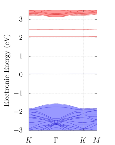
The vacuum thickness was greater than four interlayer spacings of bulk hBN (Ref. Wang, Ma, and Sun, 2017) and Van der Waals interactions were represented using the Grimme-D3 scheme (Grimme, 2011). The formation energy of a defect, , in charge state is
| (1) |
where is the total energy of the defective system, is the total energy of pristine monolayer hBN of the same size, is the change in the number of atoms of species relative to pure hBN and is the chemical potential of the species . The formation energies were calculated for N-rich conditions specified by where is half the total energy of an N2 molecule and is the energy per formula unit of monolayer hBN. is the electron chemical potential relative to the host valence band maximum (VBM), . To mitigate against the systematic errors due to periodic boundary conditions (PBC) in charged systems, we have adopted the uniform scaling of the cell sizes Komsa et al. (2014, 2018), leading to an uncertainty of the order of eV in the formation energy (Komsa et al., 2018).
Quantification of charge transfer has been approached by integrating the DOS of the heterostructure from the Fermi level to the small band gap induced by the formation of the heterostructure Prasad et al. (2023). Calculations were performed with the net spin either constrained (fixed spin) or allowed to vary during the self-consistency process (free spin). For free spin calculations, the population of the spin channels was based upon Fermi-Dirac statistics with spin-up and spin-down channels having the same self-consistent electron chemical potential.
Nudged elastic band (NEB) calculations were performed using the climbing-image method Henkelman, Uberuaga, and Jónsson (2000) for a supercell, and eleven images between the initial and final states was found to sufficiently resolve the energy surface.
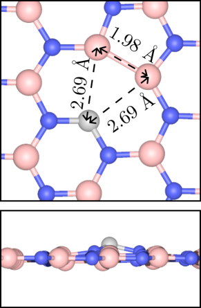
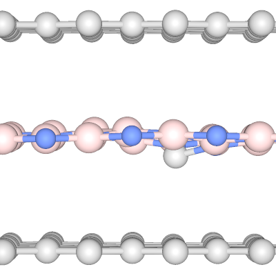
CBVN is formed when carbon substitutes for boron adjacent to a nitrogen vacancy. Interest in CBVN has focused on its potential as a source of visible single-photon emission Sajid and Thygesen (2020); Mendelson et al. (2021), particularly as it is among a class of defects with an out-of-plane intrinsic electric dipole, rendering it accessible to Stark tuning via external electric fields Tawfik et al. (2017); Scavuzzo et al. (2019). The ground state structure of the defect is a spin singlet, with symmetry due to the out-of-plane movement of the carbon atom Linderälv, Wieczorek, and Erhart (2021) (Fig. 1) . The introduction of this defect leads to one (two) occupied (unoccupied) non-degenerate defect-levels in the band gap (Fig. 1).
[] \sidesubfloat[]
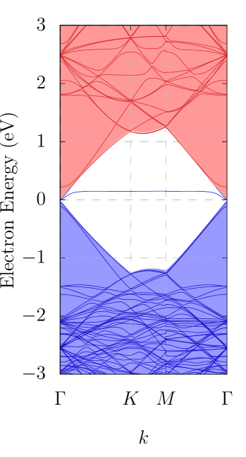
The defect when either positively and negatively charged forms a spin doublet, with symmetry geometries Mendelson et al. (2021). Taking the average position of the boron and nitrogen atoms in hBN as the location of the plane, a small, 0.18 Å, out-of-plane distortion in the positively charged defect lowers the energy by meV. This has not been captured by existing studies in literature Cheng et al. (2017). Although it is a small difference, strain effects significantly enhance the stability of the distorted arrangement, as will be discussed later. The donor and acceptor levels of CBVN were calculated at 5.1 eV and 1.3 eV below vacuum. Since the ionization energy exceeds the graphene work function (calculated at 4.3 eV Prasad et al. (2023); Ziegler et al. (2011)), charge transfer is not expected. Free spin structural relaxation of CBVN in hBN/Gr resulted in zero effective spin in the system, consistent with the defect remaining the in the neutral charge state as determined by explicit calculations of the degree of charge transfer.
A similar result was observed when an additional hBN layer was added to the system, resulting in bilayer hBN on graphene (2-hBN/Gr). No charge transfer was found and the spin-singlet state remained the ground state regardless of the layer location of the defect. This is reflected in the band structures of CBVN in both hBN/Gr and 2-hBN/Gr, Fig. 2.
The impact of an additional layer of Gr on hBN/Gr to form Gr/hBN/Gr is now reviewed. Structural relaxation of the defect-free three-layer structure yields an in-plane lattice constant of 2.48 Å, representing a +0.5% and % strains in the graphene and hBN layers relative to the isolated monolayers.
[] \sidesubfloat[]
\sidesubfloat[]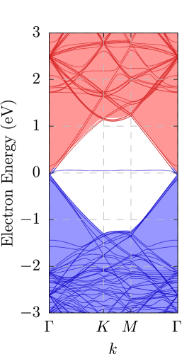 \sidesubfloat[]
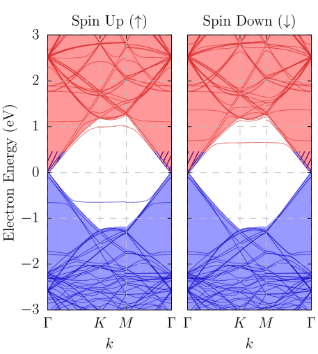
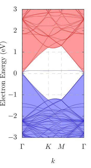
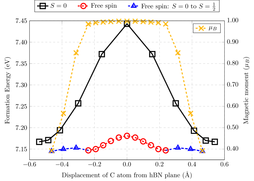
Structural relaxation performed with free spin and fixed spin () calculations resulted in the carbon atom moving out-of-plane. The carbon atom moved 0.24 nm during free spin relaxation from the hBN plane, significantly less than the 0.54 nm displacement obtained for in the fixed spin-singlet relaxation (Fig. 3 and 3). This contrasts the observation in hBN/Gr and 2-hBN/Gr where the free spin and fixed spin calculations resulted in the same structure. The reason for the difference in the structure can be understood from the magnetic moment in the free-spin case, which is , being the Bohr magneton. The calculation of charge transfer revealed that transfers from CBVN to graphene, resulting in a spin doublet. In our calculations, the self-consistently obtained spin doublet corresponding to the transfer of an electron to graphene, is only marginally stable, being just 20 meV lower than the energy obtained for the fixed spin, representing an overall spin-singlet. The calculations were repeated in and supercells, and in both cases the spin doublet is lower in energy (by 99 meV and 120 meV, respectively). We also established that the vacuum spacing does not impact the energy ordering of the and states, reflecting the absence of net polarization between the layers, as determined from the complete absence of any canceling electric field in the vacuum. As charge transfer occurred for Gr/hBN/Gr and not hBN/Gr, we suggest that the electrical levels of CBVN are modified when encapsulated by graphene.
There are two significant features of interest in this Gr/hBN/Gr system. First, it was observed that charge transfer occurs only when hBN is encapsulated in graphene. Second, the geometry of CBVN in the positive charged state in isolated hBN is nearly planar in geometry, a significant out-of-plane distortion occurs in the heterostructure.
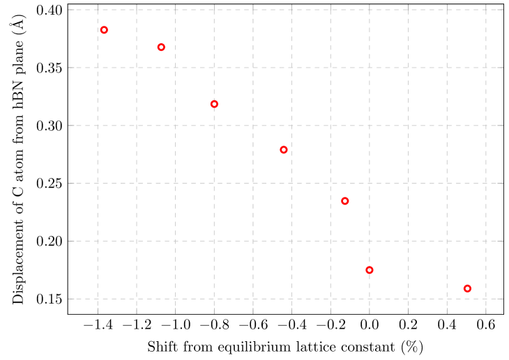
To explore the latter of these, the positively charged CBVN in isolated monolayer hBN was optimised under different biaxial strains. Figure 4 shows that increasing compressive strain leads to an increase in the displacement of the carbon atom from the hBN plane. At approximately strain, at which the lattice constant of hBN is equal to that of the heterostructure, the carbon atom is 0.38 Å from the hBN plane. At the same strain, the restriction of the carbon atom to the hBN plane results in a configuration 50 meV lower in energy, highlighting that stabilisation due to distortion, although small in unstrained hBN, has physical significance.
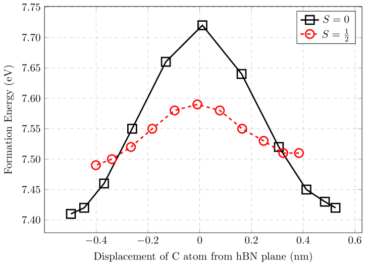
As both the spin-singlet and doublet configurations were found in the Gr/hBN/Gr heterostructure, we sought to understand the barrier to move between the two states (noting that displacement of C above and below the hBN plane are equivalent by symmetry). The barrier between the two directions of displacement was investigated for and states, the result of these NEB calculation being presented in Fig. 5.
The NEB data for the supercell show the charge-transfer, non-zero effective spin case (circles and triangles in Fig. 5), is energetically favored throughout the inversion process. The energies for the largest displacement represented by the triangles are slightly lower than the corresponding limits for the squares, and we note that this energy difference converges to around 120 meV for larger cells. The increase in the energy difference is attributed to the convergence of the effective spin from to with cell-size for the and cells, consistent with the convergence of the degree of charge transfer. For the data shown by circles the effective spin remains close to , indicating that charge-transfer is constant through this range, and the out-of-plane displacement stabilizes the defect. The barrier to move between the two orientations where charge-transfer occurs is 30 meV, whereas for the fixed spin-singlet case the barrier is 280 meV.
For comparison with a system where no charge transfer is observed, the energy profile (Fig. 6) for flipping the carbon orientations for the spin singlet and doublet states are shown for CBVN in 2-hBN/Gr, where the calculations were performed with fixed spin. At the minima in the curve, the singlet configuration is lower in energy for the same displacement of the carbon atom. Hence, a repetition of the structural relaxation with free spin converges to the equilibrium configuration. Comparing 2-hBN/Gr with Gr/hBN/Gr (Fig. 6 and 5), suggests that the donor level has been raised above the Dirac point due to the inclusion of the second graphene layer, leading to charge transfer.
We now comment on the implications for the observable optical properties based upon our findings. It is clear from Fig. 5 and 6 that the encapsulating environment has a significant effect on the CBVN charge transition levels. Similar pheonomena were previously predicted in a study on the variation of the charge transition levels (CTLs) of hBN with additional hBN layers, \ceSiO2 and diamond substrates Wang and Sundararaman (2019, 2020). Here we find that additional Gr layers have a much greater effect on the CTLs than additional hBN layers. The change may be attributed to the difference in the electric permittivities of hBN and graphene, and hence the magnitude of the electrostatic screening of the defect. As such, unlike in 2-hBN/Gr and 1-hBN/Gr systems, the charge-transfer is predicted for Gr/hBN/Gr. This will be especially relevant in systems where multilayer hBN is sandwiched between graphene gates for the application of electric fields and charge injection Noh et al. (2018); Scavuzzo et al. (2019); Yu et al. (2022); White et al. (2022).
In monolayer hBN there is a small displacement carbon atom from the hBN plane for (CBVN)+, and the effect is enhanced in the heterostructures. As illustrated by the data in Fig. 4, displacement of carbon from the hBN plane is stabilized by increasing compressive biaxial strain. Therefore, under strain or via the influence of the substrate even the positively charged defect can be tuned by an electric field perpendicular to the hBN plane, as it possesses a component of the electric dipole moment parallel to the applied field. However, the low barrier between the two equilibria of (CBVN)+ suggests that low gate voltages are sufficient for the atoms to overcome the barrier and flip to the site on the opposite side of the plane. This would invert the orientation of the dipole with respect to the field and subsequently the direction of the Stark shift. Studies on Stark tuning of hBN emitters have found ‘V’ shaped variations of zero-phonon line with applied field, which supports the occurrence of such processes Noh et al. (2018). It is also possible that some defects can possess charged configurations within the barrier of transition and act as metastable intermediate states for the transition between sites.
As the energy difference between the spin singlet and doublet configurations is meV, continued increase in the applied voltages would be likely to lead to a change in the charge state and turn the emitter dark. Even if the defect remains optically active after charge transfer, the change in the orientation of the electric dipole moment would manifest as an abrupt change in the polarization and degree of Stark shift. A low barrier to transition also increases the probability of tunneling of the carbon atom between the sites.
In this Letter we have shown that the encapsulation of hBN by graphene layers leads to dramatic modifications in the electrical levels. Using CBVN as an illustrative example, we show that the donor level shifts toward the conduction band due to additional graphene layers, leading to charge transfer. NEB modeling also shows that the barrier to the flipping of the carbon atom across the hBN plane is relatively low and would likely to lead to a ‘V’ shaped Stark shift, such as illustrated in Ref. Noh et al., 2018. It is therefore imperative that in determining viable color centers for single photon emitters that may be controlled by an external electric field, the correct charge state, strain and substrate are explicitly modeed. Also, the complex interplay between the dielectric environment and strain led to defect geometries that can differ significantly from the monolayer case and has implications on spectroscopic properties, such as the response to external electric fields and the degree of phonon coupling. The results of this work will therefore have a significant impact on the electric field, charge and strain control of quantum emitters in hBN for applications in quantum technologies.
References
- Tran et al. (2016) T. T. Tran, K. Bray, M. J. Ford, M. Toth, and I. Aharonovich, “Quantum emission from hexagonal boron nitride monolayers,” Nature Nanotechnology 11, 37–41 (2016).
- Grzeszczyk et al. (2024) M. Grzeszczyk, K. Vaklinova, K. Watanabe, T. Taniguchi, K. S. Novoselov, and M. Koperski, “Electroluminescence from pure resonant states in hBN-based vertical tunneling junctions,” Light: Science & Applications 13, 155 (2024).
- Asshoff et al. (2018) P. U. Asshoff, J. L. Sambricio, S. Slizovskiy, A. P. Rooney, T. Taniguchi, K. Watanabe, S. J. Haigh, V. Fal’ko, I. V. Grigorieva, and I. J. Vera-Marun, “Magnetoresistance in Co-hBN-NiFe tunnel junctions enhanced by resonant tunneling through single defects in ultrathin hBN barriers,” Nano Letters 18, 6954–6960 (2018).
- Prasad et al. (2024) M. K. Prasad, M. P. Taverne, C.-C. Huang, J. D. Mar, and Y.-L. D. Ho, “Hexagonal boron nitride based photonic quantum technologies,” Materials 17, 4122 (2024).
- Noh et al. (2018) G. Noh, D. Choi, J. H. Kim, D. G. Im, Y. H. Kim, H. Seo, and J. Lee, “Stark tuning of single-photon emitters in hexagonal boron nitride,” Nano Letters 18 (2018), 10.1021/acs.nanolett.8b01030.
- Xu et al. (2020) Z. Q. Xu, N. Mendelson, J. A. Scott, C. Li, I. H. Abidi, H. Liu, Z. Luo, I. Aharonovich, and M. Toth, “Charge and energy transfer of quantum emitters in 2D heterostructures,” 2D Materials (2020), 10.1088/2053-1583/ab7fc3.
- Stewart et al. (2021) J. C. Stewart, Y. Fan, J. S. Danial, A. Goetz, A. S. Prasad, O. J. Burton, J. A. Alexander-Webber, S. F. Lee, S. M. Skoff, V. Babenko, and S. Hofmann, “Quantum emitter localization in layer-engineered hexagonal boron nitride,” ACS Nano 15 (2021), 10.1021/acsnano.1c04467.
- Yu et al. (2022) M. Yu, D. Yim, H. Seo, and J. Lee, “Electrical charge control of h-bn single photon sources,” 2D Materials 9, 035020 (2022).
- Scavuzzo et al. (2019) A. Scavuzzo, S. Mangel, J. H. Park, S. Lee, D. L. Duong, C. Strelow, A. Mews, M. Burghard, and K. Kern, “Electrically tunable quantum emitters in an ultrathin graphene-hexagonal boron nitride van der Waals heterostructure,” Applied Physics Letters 114 (2019), 10.1063/1.5067385.
- Prasad et al. (2023) M. K. Prasad, O. A. Al-Ani, J. P. Goss, and J. D. Mar, “Charge transfer due to defects in hexagonal boron nitride/graphene heterostructures: An ab initio study,” Physical Review Materials 7, 094003 (2023).
- Sensoy et al. (2017) M. G. Sensoy, D. Vinichenko, W. Chen, C. M. Friend, and E. Kaxiras, “Strain effects on the behavior of isolated and paired sulfur vacancy defects in monolayer MoS2,” Physical Review B 95, 014106 (2017).
- Aschauer and Spaldin (2016) U. Aschauer and N. A. Spaldin, “Interplay between strain, defect charge state, and functionality in complex oxides,” Applied Physics Letters 109 (2016).
- Deger et al. (2022) C. Deger, S. Tan, K. Houk, Y. Yang, and I. Yavuz, “Lattice strain suppresses point defect formation in halide perovskites,” Nano Research 15, 5746–5751 (2022).
- Wang and Sundararaman (2019) D. Wang and R. Sundararaman, “Substrate effects on charged defects in two-dimensional materials,” Physical Review Materials 3 (2019), 10.1103/PhysRevMaterials.3.083803.
- Wang and Sundararaman (2020) D. Wang and R. Sundararaman, “Layer dependence of defect charge transition levels in two-dimensional materials,” Physical Review B 101 (2020), 10.1103/PhysRevB.101.054103.
- Jones and Briddon (1998) R. Jones and P. Briddon, “Chapter 6 the ab initio cluster method and the dynamics of defects in semiconductors,” in Identification of Defects in Semiconductors, Semiconductors and Semimetals, Vol. 51, edited by M. Stavola (Elsevier, 1998) pp. 287–349.
- Perdew, Burke, and Ernzerhof (1996) J. P. Perdew, K. Burke, and M. Ernzerhof, “Generalized gradient approximation made simple,” Physical Review Letters 77 (1996), 10.1103/PhysRevLett.77.3865.
- Hartwigsen, Gœdecker, and Hutter (1998) C. Hartwigsen, S. Gœdecker, and J. Hutter, “Relativistic separable dual-space gaussian pseudopotentials from h to rn,” Physical Review B 58, 3641 (1998).
- Goss, Shaw, and Briddon (2007) J. P. Goss, M. J. Shaw, and P. R. Briddon, “Marker-method calculations for electrical levels using gaussian-orbital basis sets,” in Theory of Defects in Semiconductors, Topics in Applied Physics, Vol. 104, edited by D. A. Drabold and S. K. Estreicher (Springer, Berlin/Heidelberg, 2007) pp. 69–94.
- Monkhorst and Pack (1976) H. J. Monkhorst and J. D. Pack, “Special points for brillouin-zone integrations,” Physical Review B 13 (1976), 10.1103/PhysRevB.13.5188.
- Wang, Ma, and Sun (2017) J. Wang, F. Ma, and M. Sun, “Graphene, hexagonal boron nitride, and their heterostructures: properties and applications,” RSC Advances 7 (2017), 10.1039/c7ra00260b.
- Grimme (2011) S. Grimme, “Density functional theory with london dispersion corrections,” Wiley Interdisciplinary Reviews: Computational Molecular Science 1, 211–228 (2011).
- Komsa et al. (2014) H.-P. Komsa, N. Berseneva, A. V. Krasheninnikov, and R. M. Nieminen, “Charged point defects in the flatland: Accurate formation energy calculations in two-dimensional materials,” Physical Review X 4, 031044 (2014).
- Komsa et al. (2018) H.-P. Komsa, N. Berseneva, A. V. Krasheninnikov, and R. M. Nieminen, “Erratum: Charged point defects in the flatland: Accurate formation energy calculations in two-dimensional materials [phys. rev. x 4, 031044 (2014)],” Physical Review X 8, 039902 (2018).
- Henkelman, Uberuaga, and Jónsson (2000) G. Henkelman, B. P. Uberuaga, and H. Jónsson, “A climbing image nudged elastic band method for finding saddle points and minimum energy paths,” The Journal of Chemical Physics 113, 9901–9904 (2000).
- Sajid and Thygesen (2020) A. Sajid and K. S. Thygesen, “VNCB defect as source of single photon emission from hexagonal boron nitride,” 2D Materials 7, 031007 (2020).
- Mendelson et al. (2021) N. Mendelson, D. Chugh, J. R. Reimers, T. S. Cheng, A. Gottscholl, H. Long, C. J. Mellor, A. Zettl, V. Dyakonov, P. H. Beton, S. V. Novikov, C. Jagadish, H. H. Tan, M. J. Ford, M. Toth, C. Bradac, and I. Aharonovich, “Identifying carbon as the source of visible single-photon emission from hexagonal boron nitride,” Nature Materials 20 (2021), 10.1038/s41563-020-00850-y.
- Tawfik et al. (2017) S. A. Tawfik, S. Ali, M. Fronzi, M. Kianinia, T. T. Tran, C. Stampfl, I. Aharonovich, M. Toth, and M. J. Ford, “First-principles investigation of quantum emission from hBN defects,” Nanoscale 9 (2017), 10.1039/c7nr04270a.
- Linderälv, Wieczorek, and Erhart (2021) C. Linderälv, W. Wieczorek, and P. Erhart, “Vibrational signatures for the identification of single-photon emitters in hexagonal boron nitride,” Physical Review B 103, 115421 (2021).
- Cheng et al. (2017) G. Cheng, Y. Zhang, L. Yan, H. Huang, Q. Huang, Y. Song, Y. Chen, and Z. Tang, “A paramagnetic neutral CBVN center in hexagonal boron nitride monolayer for spin qubit application,” Computational Materials Science 129, 247–251 (2017).
- Ziegler et al. (2011) D. Ziegler, P. Gava, J. Güttinger, F. Molitor, L. Wirtz, M. Lazzeri, A. Saitta, A. Stemmer, F. Mauri, and C. Stampfer, “Variations in the work function of doped single-and few-layer graphene assessed by Kelvin probe force microscopy and density functional theory,” Physical Review B—Condensed Matter and Materials Physics 83, 235434 (2011).
- White et al. (2022) S. J. U. White, T. Yang, N. Dontschuk, C. Li, Z.-Q. Xu, M. Kianinia, A. Stacey, M. Toth, and I. Aharonovich, “Electrical control of quantum emitters in a Van der Waals heterostructure,” Light: Science & Applications 11, 186 (2022).