Hydrophilic direct bonding of (100) diamond and a deposited SiO2 substrates
Abstract
Diamond has emerged as a leading material for solid-state spin quantum systems and extreme environment electronics. However, a major limitation is that most diamond devices and structures are fabricated using bulk diamond plates. The absence of a suitable diamond-on-insulator (DOI) substrate hinders the advanced nanofabrication of diamond quantum and electronic devices, posing a significant roadblock to large-scale, on-chip diamond quantum photonics and electronics systems. In this work, we demonstrate the direct bonding of (100) single-crystal (SC) diamond plates to PECVD-grown SiO2/Si substrates at low temperatures and atmospheric conditions. The surfaces of the SiO2 and diamond plates are then activated using oxygen plasma and piranha solution, respectively. Bonding occurs when the substrates are brought into contact with water in between and annealed at 200∘C under atmospheric conditions, resulting in a DOI substrate. We systematically studied the influence of piranha solution treatment time and diamond surface roughness on the shear strength of the bonded substrate, devising an optimal bonding process that achieves a high yield rate of 90 and a maximum shear strength of 9.6 MPa. X-ray photoelectron spectroscopy (XPS) was used for quantitative analysis of the surface chemicals at the bonding interface. It appears that the amount of -OH bindings increases with the initial roughness of the diamond, facilitating the strong bonding with the SiO2. This direct bonding method will pave the way for scalable manufacturing of diamond nanophotonic devices and enable large-scale integration of diamond quantum and electronic systems.
Diamond is a promising material for quantum applicationsDoherty et al. (2013); Prawer and Aharonovich (2018); Sar, Taminiau, and Hanson (2021); Ruf et al. (2021). Spins in diamond color-centers such as NV center have shown significant potential in quantum technologiesDoherty et al. (2013); Prawer and Aharonovich (2018); Bradley et al. (2022). Their long spin coherence timesBar-Gill et al. (2013); Abobeih et al. (2018), optical readout capabilities, high operational temperaturesIwasaki et al. (2017), and suitability for nanofabrication techniques and nanophotonic structures make them highly attractive for quantum applications. Recently, tin-vacancy (SnV) centersIwasaki et al. (2017); Rosenthal et al. (2024); Debroux et al. (2021) in diamond showed their reduced sensitivity to environmental noise and compatibility with nanofabricated devicesRugar et al. (2020); Kuruma et al. (2021a); Pasini et al. (2024); Chen et al. (2024), enhancing their versatility for large-scale quantum computersIshihara et al. (2021) and communication Ruf et al. (2021); Debroux et al. (2021); Chen et al. (2024). Diamond is also an exceptional material for power and extreme environment electronicsPerez et al. (2020); Donato et al. (2020); Hasan et al. (2024); Liang and Shigekawa (2024); Angelone and Verona (2021); Khanna (2023); Umezawa (2022) due to its superior electronic and thermal propertiesZhang et al. (2023a), including high electrical breakdown field strength, exceptional carrier mobility, and excellent thermal conductivityPerez et al. (2020); Donato et al. (2020); Hasan et al. (2024); Angelone and Verona (2021). These characteristics make diamond an ideal candidate for devices requiring efficient heat dissipation and high-power handling capabilitiesPerez et al. (2020); Donato et al. (2020); Hasan et al. (2024); Angelone and Verona (2021); Khanna (2023); Umezawa (2022); Zhang et al. (2023a). Beyond its electronic advantages, diamond also possesses outstanding optical propertiesMildren (2013), such as a high refractive index and wide bandgapHiscocks et al. (2008), along with superior mechanical properties like a high Young’s modulusHess (2012).
Despite these promising attributes, scalable integration of diamond-based systems remains elusive, especially in quantum technologies. This challenge is primarily due to the lack of appropriate substrates. Epitaxial growth or deposition of high-quality single-crystal diamond is extremely challenging Kasu (2016); Schreck et al. (2017). Moreover, commercially available single-crystal diamond substrates are small—typically less than a centimeter or even just a few millimeters due to the HTHP processYunin et al. (2018); Li et al. (2019) —and most diamond quantum devices to date are fabricated from these bulk diamond substrates Burek et al. (2012); Khanaliloo et al. (2015); Toros et al. (2020); Rugar et al. (2020); Kuruma et al. (2021a); Pasini et al. (2024); Chen et al. (2024). In quantum photonic applications, two critical factors are essential. First, the quality of the interface is crucial, as any damage, trapped charges, or poor interface quality can significantly degrade the optical properties of color center qubits, reduce coherence times, and impair overall system performanceSangtawesin et al. (2019); Rodgers et al. (2021); Orphal-Kobin et al. (2023); Kumar et al. (2024). Second, enhancing the optical performance of diamond color center qubits often requires integrating photonic devices. This necessitates the use of diamond-on-insulator (DOI) substrates. For high-quality device manufacturing and scalable integration in both quantum technologies and power electronics, DOI substrates would be a key component. The method for producing DOI structures is to use wafer or substrate bonding technologies to attach diamond plates to different substrate materials.
Bonding Type Substrates bonded Diamond Surface treatment Process conditions (Roughness, Pressure, Temperature) Bonded Area (up to) Bonding Strength Remark/critical issues for Quantum applications Ref. Hydrophilic Diamond (111), Various semiconductor substrates (InP, Si) and SiO2/Si (thermal or native) Oxidizing solutions, such as H2SO4/H2O2 and NH3/H2O2 mixtures, C, Atm < 0.5 nm, 0 to 1 MPa Load, to C mm to MPa Amorphous layer to 5 nm, Not suitable for photonics Matsumae et al. (2020a, b, c, 2019a); Fukumoto et al. (2020, 2020, 2021); Liang and Shigekawa (2024); Matsumae et al. (2021a); Liang et al. (2022); Matsumae et al. (2023, 2020d) Hydrophilic Diamond (100), Si Oxidizing solutions, H2SO4/H2O2 and NH3/H2O2 mixtures, C, Atm to 0.2 nm, Pressure MPa, to C mm 1.7 MPa Amorphous layer to 5 nm, weaker bond strength, Not suitable for photonics Matsumae et al. (2021b); Okita et al. (2023) Surface activated bonding (SAB) Diamond (100), Sapphire Ar beam irradiation, High vac Pa < 0.2 nm, 20 MPa, RT mm MPa 300 nm amorphous layer, Diffusion of bonding elements, Poor interface for quantum applications Miyatake et al. (2023) Adhesive Diamond substrates, Si or SiO2/Si substrates Boiling Piranha solution < 0.4 nm or 2 nm, HSQ adhesion, Pressure 0 to 105 kPa, 500 to 600∘C, Membrane synthesis (smart-cut) and transfer m to mm Strong, but not measured Negligible amorphous layer, HSQ background fluorescence, Poor scalability and integration Tao et al. (2014a); Kuruma et al. (2021b); Jung et al. (2016); Guo et al. (2021, 2023a) Plasma activation based (PAB) Diamond to various substrates (Si, fused silica, Sapphire, thermal oxide, lithium niobate) O2 plasma ashing (O2 flow - 200 sccm and RF power - 600 W for 150 s) for hydrophilic surface < 1 nm, Smart-cut and transfer, Heating up to C, No pressure, C anneal m Strong, but not measured Sub-nm interfacial layer, nm uniformity, DOI Film nm, Poor scalability and integration Guo et al. (2023b); Ding et al. (2024) Hydrophilic Diamond (100), PECVD SiO2/Si Oxidizing solutions - H2SO4/H2O2 mixtures, C, Atm 1.5 to 5 nm, No pressure, C mm MPa Negligible intermediate layer, Suitable for quantum & photonics, Scalable In this work
Bonding methods are usually categorized based on the use of intermediate materials/layers to attach the substrates: non-direct and direct bonding. A variety of bonding techniques, including Surface Activated Bonding (SAB)Liang et al. (2017); Miyatake et al. (2023); Liang et al. (2019a), , Atomic Diffusion Bonding (ADB) Matsumae et al. (2018), Compression Bonding Delmas et al. (2024), Metallic Bonding Wang et al. (2023), Adhesive Bonding Heupel et al. (2020); Bleiker et al. (2017); Tao et al. (2014a); Kuruma et al. (2021b); Jung et al. (2016); Guo et al. (2021, 2023a), Plasma Activated Bonding (PAB) Guo et al. (2023b); Ding et al. (2024), Fusion Bonding Yushin et al. (2002a); Piracha et al. (2016a), and Hydrophilic Direct Bonding Matsumae et al. (2019a, 2020e, 2020a, 2020f, 2021b); Okita et al. (2023); Fukumoto et al. (2020, 2020, 2021); Liang and Shigekawa (2024); Matsumae et al. (2021a); Liang et al. (2022); Matsumae et al. (2023, 2020d), have been employed to attach diamond plates to other substrates Zhao and Hu (2024). A summary of direct bonding techniques used for diamond substrates is provided in Table 1. Most of these approaches can lead to significant interface issues, such as amorphization, metallization, or defects, which make the bonded substrates unsuitable for complex, large-scale 3D integration processes Ishihara et al. (2021) and for quantum applications. The direct bonding methods are the most promising for producing DOI-type substrates necessary for on-chip diamond-based quantum systems. Matsumae et al., showed that OH-terminated diamond (111) and Si or SiO2/Si substrates are chemically bonded through a dehydration reactionMatsumae et al. (2020a, b, c, 2019a). However, the previous studies have been limited to extremely smooth (< 0.5 nm) diamond (111) substrates and thermally grown or native SiO2 interface layers. It should be noted that (100) sc-diamond is widely available and suitable, especially for group IV color-centers in diamond such as SnV center. Also, (111) sc-diamond has even smaller size due to cutting along (111) plane of the (100) diamond plates. Furthermore, the thermally grown SiO2 requires high-temperature processes and hence limits the applications, such as heterogeneous integration of diamond on temperature-sensitive materials. In this work, we have achieved a hydrophilic direct bonding of diamond (100) substrates onto SiO2 layers grown by PECVD on silicon wafers, by optimizing the surface roughness of diamond. Additionally, we have examined the chemical composition of diamond surfaces after Piranha treatment and analyzed the influence of treatment conditions on the shear strength of the bonded interfaces.
The experimental process involves the following steps: First, a (100)-oriented diamond substrate with different roughness undergoes an immersion in Piranha solution (H2SO4 and H2O2 in a 3:1 ratio) at 75∘C for various treatment times to achieve OH termination. After treatment, the diamond substrate is rinsed in deionized water for 5–10 minutes. SiO2/Si wafers are prepared separately, a 300 nm layer of silicon dioxide is deposited onto the Si wafer using a PECVD reactor (Novellus Concept 1) at a temperature of 400∘C. After the deposition, the SiO2/Si wafers are diced into substrates, which are OH-terminated using plasma at 1000 W for 5 minutes. This OH-termination of SiO2 through plasma treatment facilitates chemical bonding between the diamond and SiO2/Si substrates in the presence of water. Next, the diamond substrate is placed atop the /Si substrate in the presence of water without needing any external pressure. The assembled substrates are stored under atmospheric conditions (20∘C and 40% relative humidity) for 3 days to remove excess water molecules. Finally, the specimens are annealed at 200∘ for 24 hours to initiate the reaction Matsumae et al. (2019a), which describes the bond formation process between diamond and interface:
| (1) |
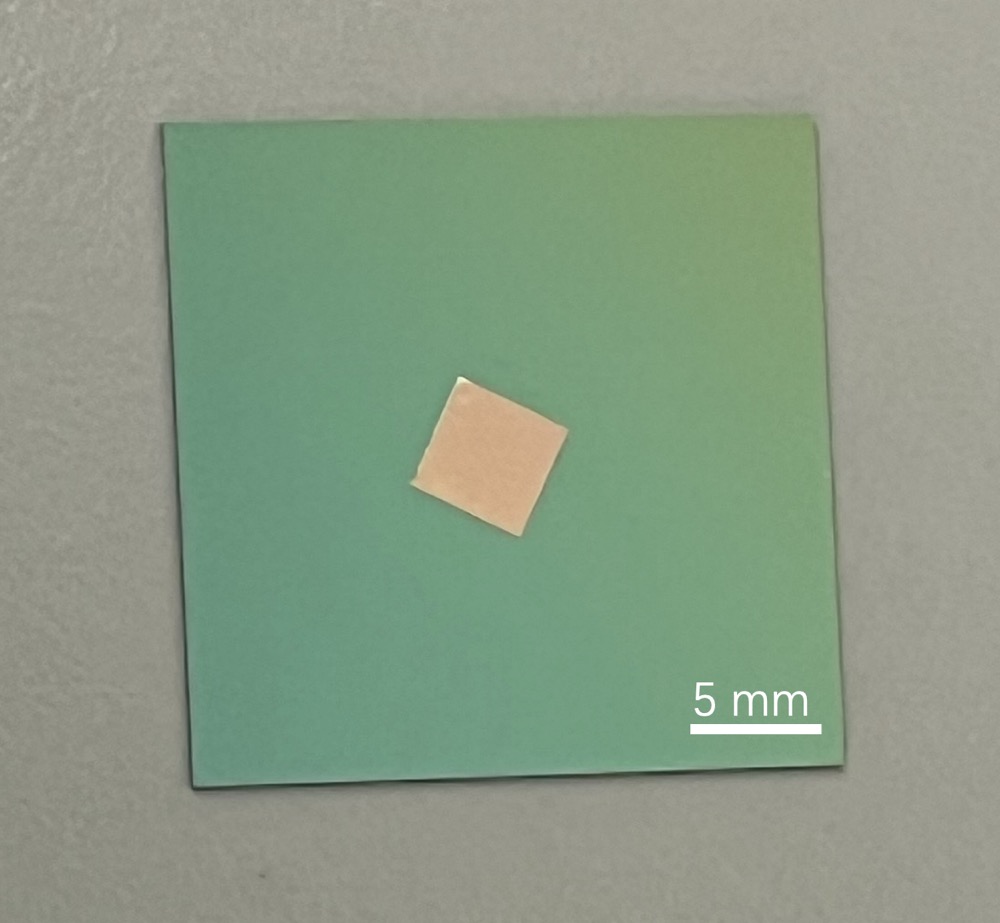
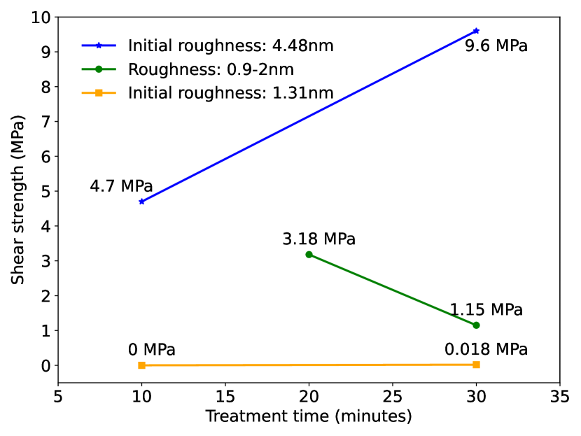
Figure 1 presents a photograph of a (100) diamond substrate bonded to a SiO2/Si substrate after Piranha treatment at 75∘C for 30 minutes. In the image, the blue substrate is SiO2/Si, and the transparent substrate is diamond (4 mm 4 mm, thickness 50 m) and there is no visible fringes. This result demonstrates that diamond cleaned with proper Piranha solution can be effectively bonded to a SiO2/Si substrate without visible air gaps. Figure2 shows the shear strength of diamond substrates bonded to 300 nm SiO2/Si. We have utilized three types of diamond substrates with different initial roughnesses—4.48 nm, 2 nm, and 1.31 nm. Surface roughness has been evaluated using an atomic force microscope (AFM, Bruker). After successful bonding, bonding strength has been measured using a Nordson DAGE 4000Plus die shear tester. The testing procedure adheres to the guidelines specified in the MIL-STD-883 standard. The rough diamonds with an initial roughness of 4.48 nm exhibit the highest shear strength (4.7 MPa and 9.6 MPa) compared to the other two experimental groups, and there is an increasing trend with longer treatment time. In contrast, the smooth diamonds with an initial roughness of 1.31 nm are not able to be bonded even with the long treatment time. This contrasts with findings in previous worksMatsumae et al. (2020a, b, c, 2019a), which show that only very smooth diamond (111) substrates can be bonded. Interestingly, the intermediate group with a roughness of 2 nm exhibits a decreasing trend in the moderate shear strength as the treatment time increases. This may be because when the diamond roughness reaches a certain threshold, roughness becomes the dominant factor affecting bonding, favoring rougher surfaces. Conversely, when the diamond roughness is below that threshold, other factors, such as surface chemistry and activation, play more significant roles.
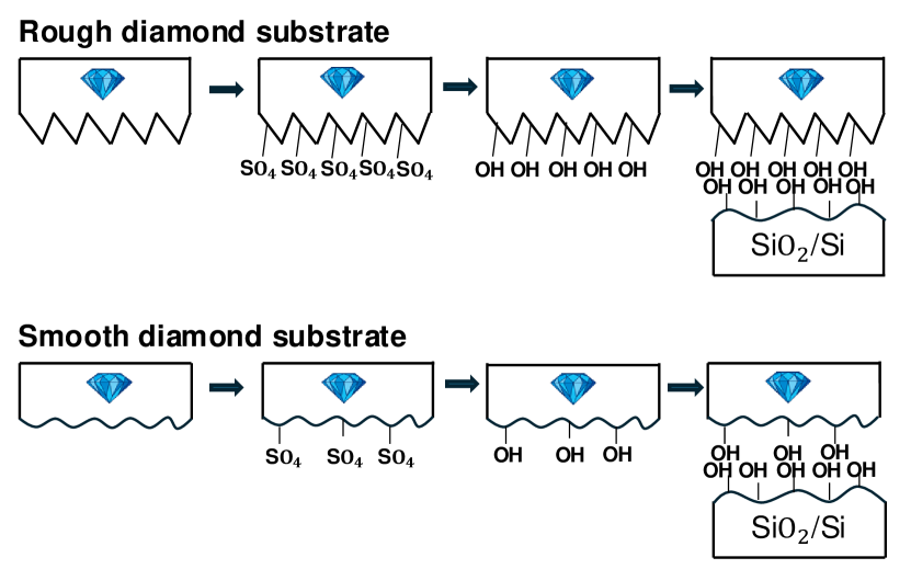
Chemical composition of the substrates have been identified as critical factors for successful bonding. The chemical composition of the treated diamond surface has been investigated using X-ray photoelectron spectroscopy (XPS). Analyses have been carried out using a PHI TFA XPS spectrometer (Physical Electronics Inc.), equipped with an X-ray Al K monochromatic source ( eV). The vacuum during XPS analysis has been maintained at approximately mbar. During measurements, the analyzed area has a diameter of 0.4 mm and a corresponding depth of analysis in the range of 3–5 nm. High-resolution narrow multiplex scans of C1s, O1s, S2p3, and Si2p peaks have been collected with pass energies of 23.5 eV and a resolution of 0.2 eV at a take-off angle of C. The acquired spectra have been processed using MultiPak v8.0 (Physical Electronics Inc.). Figure4 schematically illustrates the possible mechanism of diamond direct bonding.
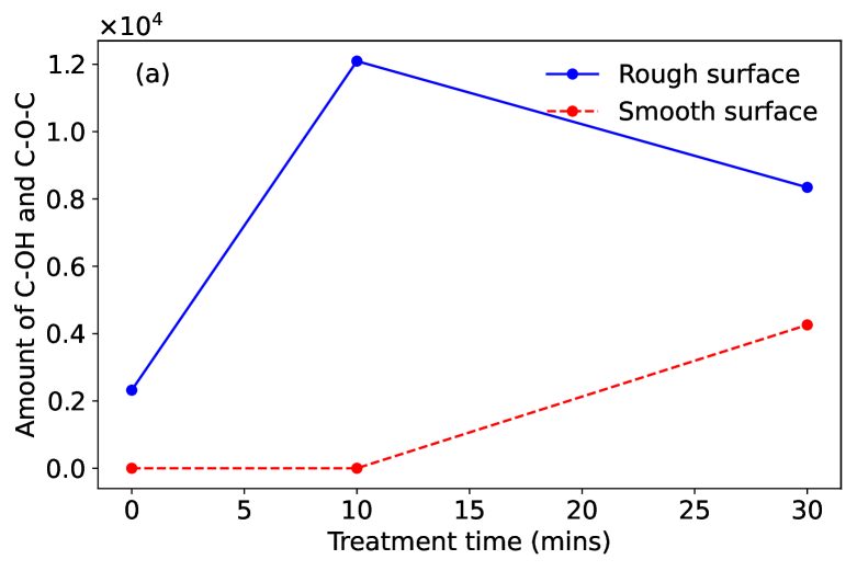
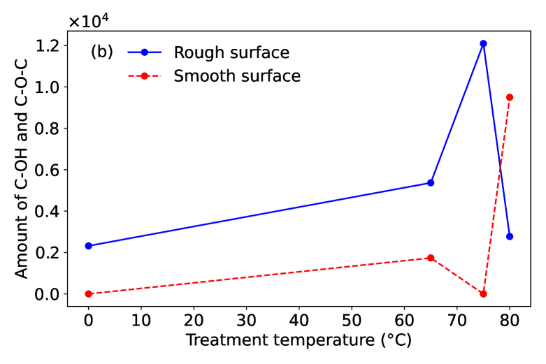
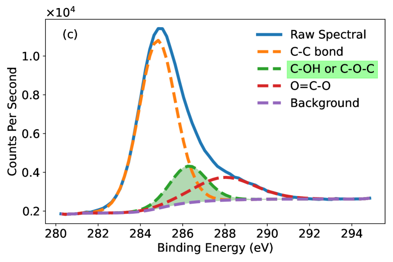
Our XPS results, plotted in Figure3, support this mechanism by illustrating the variation of C–OH groups as a function of treatment time and temperature. We observe that rough surfaces tend to exhibit a higher amount of C–OH groups compared to smooth surfaces. The inset spectra in Figure3(a) show the fitted peaks of the C1s region from an XPS spectrum of a diamond sample treated with Piranha solution for 10 minutes at 75∘C. The fitted peaks are attributed to C–C, O=C–O, and C–OH or C–O–C bonds (note that C–OH and C–O–C cannot be differentiated by XPSFukumoto et al. (2020)). Additionally, Figure 3(a) includes a line chart illustrating the variation in the quantity of C–OH or C–O–C bonds with different treatment durations, comparing rough and smooth surfaces of diamond substrates. These substrates have one side polished to a roughness less than 2 nm. Before wet treatment, the rough surface shows the presence of C–OH or C–O–C bonds, while the smooth surface has no signal in this region. This signal can be attributed to the native C–O–C bonds existing on the rough surface. After Piranha treatment, diamond surfaces are terminated with newly generated –OH groups. To mitigate the influence of surface roughness on the detected surface chemical groups, we focus on the data from the smooth sides, as they have similar roughness values of around 2 nm. Analysis of the smooth surface data reveals that the amount of –OH groups increases with longer treatment time. Additionally, the temperature of the Piranha solution significantly affects the generation of –OH groups. In the temperature range of 65–80∘C, treatment at 80∘C appears to be more effective in promoting the generation of –OH groups. Therefore, Piranha treatment time and temperature are two dominant factors in surface activation. Moreover, rough surfaces tend to be more readily terminated with –OH groups. Figure 3(b) shows the variation of Piranha-terminated –OH groups as a function of treatment temperature, indicating that a 75∘C Piranha bath is preferred as the optimal condition considering both effectiveness and practical considerations. Figure 3(c) shows a deconvoluted spectrum example of rough diamond surface treated in Piranha solution for 10 mins under 75∘C. C-C, C-OH (or C-O-C), O=C-O peaks show up in the spectrum, and C-OH groups provides the source of direct bonding. To validate our conclusions, it is good to compare XPS measurements with bonding strength measurements. The amount of –OH groups directly affects the strength of the bonding. Therefore, aligning the results of the –OH group quantification with bonding strength under different treatment conditions provides further confirmation of our findings.
Our combined XPS and bonding strength measurements suggest that both surface roughness and the generation of –OH groups are critical in determining the bonding strength. While higher roughness facilitates the formation of more –OH groups, leading to stronger bonds, overly smooth surfaces may lack sufficient reactive sites for effective bonding. Before treatment, the rough surfaces of the diamond are covered with native C–C and C–O–C groups, while the smooth surfaces are only covered with native C–C groups. When the diamond surface is treated with Piranha solution, hydroxyl (C–OH) groups are generated via dehydration reactions. On the one hand, the rough surface has more available areas to be terminated with –OH groups due to its higher surface area. On the other hand, the native C–O–C groups, which have the same valence state as C–OH, provide an additional source for C–OH generation. This leads to a significantly higher generation of –OH groups on rough surfaces compared to smooth surfaces. In the final step, the chemical reaction between a large amount of the –OH groups for the initially rough surface on the diamond and SiO2 surfaces forms a strong bond between the two substrates.
In conclusion, We have demonstrated a hydrophilic direct bonding of (100) single-crystal diamond plates—with thicknesses of 50 m and 500 m—to PECVD-grown SiO2/Si substrates under low-temperature and atmospheric conditions, creating diamond-on-insulator (DOI) substrates suitable for advanced quantum and electronic devices. Our findings reveal that surface roughness in the range of 2 nm to 5 nm and chemical composition are critical for strong bonding; specifically, relatively rough diamond surfaces (with roughness around 4.48 nm) generate more hydroxyl (–OH) groups after Piranha treatment due to their higher surface area and the presence of native C–O–C groups, leading to stronger chemical bonds at the interface. By optimizing Piranha treatment conditions and surface roughness within this range, we achieved a 90% bonding yield and a maximum shear strength of 9.6 MPa. This direct bonding method addresses the need for scalable DOI substrates, paving the way for large-scale integration of diamond-based systems. Future work will focus on refining this technique to produce photonic-grade DOI substrates and exploring its applicability to larger substrates and other insulating materials, thereby advancing diamond nanophotonic devices and on-chip quantum technologies.
Acknowledgements.
We gratefully acknowledge support from the joint research program “Modular quantum computers” by Fujitsu Limited and Delft University of Technology, co-funded by the Netherlands Enterprise Agency under project number PPS2007.Data Availability Statement
The data that support the findings of this study are available from the corresponding authors upon reasonable request.
References
- Doherty et al. (2013) M. W. Doherty, N. B. Manson, P. Delaney, F. Jelezko, J. Wrachtrup, and L. C. Hollenberg, Physics Reports 528, 1 (2013).
- Prawer and Aharonovich (2018) S. Prawer and I. Aharonovich, Quantum Information Processing with Diamond: Principles and Applications, 1st ed. (Woodhead Publishing, Limited, 2018).
- Sar, Taminiau, and Hanson (2021) T. V. D. Sar, T. H. Taminiau, and R. Hanson, Photoniques , 44 (2021).
- Ruf et al. (2021) M. Ruf, N. H. Wan, H. Choi, D. Englund, and R. Hanson, Journal of Applied Physics 130, 070901 (2021).
- Bradley et al. (2022) C. E. Bradley, S. W. d. Bone, P. F. W. Möller, S. Baier, M. J. Degen, S. J. H. Loenen, H. P. Bartling, M. Markham, D. J. Twitchen, R. Hanson, D. Elkouss, and T. H. Taminiau, npj Quantum Information 8, 122 (2022).
- Bar-Gill et al. (2013) N. Bar-Gill, L. M. Pham, A. Jarmola, D. Budker, and R. L. Walsworth, Nature Communications 4, 1743 (2013).
- Abobeih et al. (2018) M. H. Abobeih, J. Cramer, M. A. Bakker, N. Kalb, M. Markham, D. J. Twitchen, and T. H. Taminiau, Nature Communications 9, 2552 (2018).
- Iwasaki et al. (2017) T. Iwasaki, Y. Miyamoto, T. Taniguchi, P. Siyushev, M. H. Metsch, F. Jelezko, and M. Hatano, Phys. Rev. Lett. 119, 253601 (2017).
- Rosenthal et al. (2024) E. I. Rosenthal, S. Biswas, G. Scuri, H. Lee, A. J. Stein, H. C. Kleidermacher, J. Grzesik, A. E. Rugar, S. Aghaeimeibodi, D. Riedel, M. Titze, E. S. Bielejec, J. Choi, C. P. Anderson, and J. Vučković, Phys. Rev. X 14, 041008 (2024).
- Debroux et al. (2021) R. Debroux, C. P. Michaels, C. M. Purser, N. Wan, M. E. Trusheim, J. Arjona Martínez, R. A. Parker, A. M. Stramma, K. C. Chen, L. de Santis, E. M. Alexeev, A. C. Ferrari, D. Englund, D. A. Gangloff, and M. Atatüre, Phys. Rev. X 11, 041041 (2021).
- Rugar et al. (2020) A. E. Rugar, C. Dory, S. Aghaeimeibodi, H. Lu, S. Sun, S. D. Mishra, Z.-X. Shen, N. A. Melosh, and J. Vučković, ACS Photonics 7, 2356 (2020).
- Kuruma et al. (2021a) K. Kuruma, B. Pingault, C. Chia, D. Renaud, P. Hoffmann, S. Iwamoto, C. Ronning, and M. Lončar, Applied Physics Letters 118, 230601 (2021a).
- Pasini et al. (2024) M. Pasini, N. Codreanu, T. Turan, A. Riera Moral, C. F. Primavera, L. De Santis, H. K. C. Beukers, J. M. Brevoord, C. Waas, J. Borregaard, and R. Hanson, Phys. Rev. Lett. 133, 023603 (2024).
- Chen et al. (2024) K. C. Chen, I. Christen, H. Raniwala, M. Colangelo, L. D. Santis, K. Shtyrkova, D. Starling, R. Murphy, L. Li, K. Berggren, P. B. Dixon, M. Trusheim, and D. Englund, Optica Quantum 2, 124 (2024).
- Ishihara et al. (2021) R. Ishihara, J. Hermias, S. Yu, K. Y. Yu, Y. Li, S. Nur, T. Iwai, T. Miyatake, K. Kawaguchi, Y. Doi, and S. Sato, in 2021 IEEE International Electron Devices Meeting (IEDM) (IEEE, San Francisco, CA, USA, 2021) pp. 14.5.1–14.5.4.
- Perez et al. (2020) G. Perez, A. Maréchal, G. Chicot, P. Lefranc, P.-O. Jeannin, D. Eon, and N. Rouger, Diamond and Related Materials 110, 108154 (2020).
- Donato et al. (2020) N. Donato, N. Rouger, J. Pernot, G. Longobardi, and F. Udrea, Journal of Physics D: Applied Physics 53, 093001 (2020).
- Hasan et al. (2024) M. M. Hasan, C. Wang, N. Pala, and M. Shur, Nanomaterials 14 (2024), 10.3390/nano14050460.
- Liang and Shigekawa (2024) J. Liang and N. Shigekawa, “Direct Bonding of Diamond and Dissimilar Materials for Fabricating High Performace Power Devices,” in Novel Aspects of Diamond II: Science and Technology, edited by S. Mandal and N. Yang (Springer Nature Switzerland, Cham, 2024) Chap. 9, pp. 237–268.
- Angelone and Verona (2021) M. Angelone and C. Verona, Journal of Nuclear Engineering 2, 422 (2021).
- Khanna (2023) V. K. Khanna, “Diamond electronics for ultra-hot environments,” in Extreme-Temperature and Harsh-Environment Electronics (Second Edition), 2053-2563 (IOP Publishing, 2023) Chap. 10, pp. 10–1 to 10–33.
- Umezawa (2022) H. Umezawa, in 2022 6th IEEE Electron Devices Technology & Manufacturing Conference (EDTM) (2022) pp. 297–299.
- Zhang et al. (2023a) C. Zhang, R. D. Vispute, K. Fu, and C. Ni, Journal of Materials Science 58, 3485 (2023a).
- Mildren (2013) R. P. Mildren, “Intrinsic optical properties of diamond,” in Optical Engineering of Diamond (John Wiley & Sons, Ltd, 2013) Chap. 1, pp. 1–34.
- Hiscocks et al. (2008) M. P. Hiscocks, K. Ganesan, B. C. Gibson, S. T. Huntington, F. Ladouceur, and S. Prawer, Optics Express 16, 19512 (2008).
- Hess (2012) P. Hess, Journal of Applied Physics 111, 051101 (2012).
- Kasu (2016) M. Kasu, Progress in Crystal Growth and Characterization of Materials 62, 317 (2016), special Issue: Recent Progress on Fundamentals and Applications of Crystal Growth; Proceedings of the 16th International Summer School on Crystal Growth (ISSCG-16).
- Schreck et al. (2017) M. Schreck, S. Gsell, R. Brescia, and M. Fischer, Scientific Reports 7, 44462 (2017).
- Yunin et al. (2018) P. A. Yunin, P. V. Volkov, Y. N. Drozdov, A. V. Koliadin, S. A. Korolev, D. B. Radischev, E. A. Surovegina, and V. I. Shashkin, Semiconductors 52, 1432 (2018).
- Li et al. (2019) Y. Li, C. Wang, L. Chen, L. Guo, Z. Zhang, C. Fang, and H. Ma, RSC Advances 9, 32205 (2019).
- Burek et al. (2012) M. J. Burek, N. P. de Leon, B. J. Shields, B. J. M. Hausmann, Y. Chu, Q. Quan, A. S. Zibrov, H. Park, M. D. Lukin, and M. Lončar, Nano Letters 12, 6084 (2012), pMID: 23163557.
- Khanaliloo et al. (2015) B. Khanaliloo, M. Mitchell, A. C. Hryciw, and P. E. Barclay, Nano Letters 15, 5131 (2015), pMID: 26134379.
- Toros et al. (2020) A. Toros, M. Kiss, T. Graziosi, S. Mi, R. Berrazouane, M. Naamoun, J. Vukajlovic Plestina, P. Gallo, and N. Quack, Diamond and Related Materials 108, 107839 (2020).
- Sangtawesin et al. (2019) S. Sangtawesin, B. L. Dwyer, S. Srinivasan, J. J. Allred, L. V. H. Rodgers, K. De Greve, A. Stacey, N. Dontschuk, K. M. O’Donnell, D. Hu, D. A. Evans, C. Jaye, D. A. Fischer, M. L. Markham, D. J. Twitchen, H. Park, M. D. Lukin, and N. P. de Leon, Phys. Rev. X 9, 031052 (2019).
- Rodgers et al. (2021) L. V. H. Rodgers, L. B. Hughes, M. Xie, P. C. Maurer, S. Kolkowitz, A. C. B. Jayich, and N. P. d. Leon, MRS Bulletin 46, 623 (2021).
- Orphal-Kobin et al. (2023) L. Orphal-Kobin, K. Unterguggenberger, T. Pregnolato, N. Kemf, M. Matalla, R.-S. Unger, I. Ostermay, G. Pieplow, and T. Schröder, Phys. Rev. X 13, 011042 (2023).
- Kumar et al. (2024) R. Kumar, S. Mahajan, F. Donaldson, S. Dhomkar, H. J. Lancaster, C. Kalha, A. A. Riaz, Y. Zhu, C. A. Howard, A. Regoutz, and J. J. L. Morton, ACS Photonics 11, 1244 (2024).
- Matsumae et al. (2020a) T. Matsumae, Y. Kurashima, H. Umezawa, and H. Takagi, Japanese Journal of Applied Physics 59, SBBA01 (2020a).
- Matsumae et al. (2020b) T. Matsumae, Y. Kurashima, H. Umezawa, and H. Takagi, Scripta Materialia 175, 24 (2020b).
- Matsumae et al. (2020c) T. Matsumae, Y. Kurashima, H. Umezawa, and H. Takagi, in 2020 IEEE 70th Electronic Components and Technology Conference (ECTC) (2020) pp. 1436–1441.
- Matsumae et al. (2019a) T. Matsumae, Y. Kurashima, H. Umezawa, and H. Takagi, in 2019 6th International Workshop on Low Temperature Bonding for 3D Integration (LTB-3D) (IEEE, Kanazawa, Japan, 2019) pp. 70–70.
- Fukumoto et al. (2020) S. Fukumoto, T. Matsumae, Y. Kurashima, H. Takagi, H. Umezawa, M. Hayase, and E. Higurashi, Applied Physics Letters 117, 201601 (2020).
- Fukumoto et al. (2021) S. Fukumoto, T. Matsumae, Y. Kurashima, H. Takagi, H. Umezawa, M. Hayase, and E. Higurashi, in 2021 International Conference on Electronics Packaging (ICEP) (2021) pp. 41–42.
- Matsumae et al. (2021a) T. Matsumae, R. Takigawa, Y. Kurashima, H. Takagi, and E. Higurashi, Scientific Reports 11, 11109 (2021a), publisher: Nature Publishing Group.
- Liang et al. (2022) J. Liang, Y. Nakamura, Y. Ohno, Y. Shimizu, Y. Nagai, H. Wang, and N. Shigekawa, Functional Diamond 1, 110 (2022), publisher: Taylor & Francis _eprint: https://doi.org/10.1080/26941112.2020.1869435.
- Matsumae et al. (2023) T. Matsumae, S. Okita, S. Fukumoto, M. Hayase, Y. Kurashima, and H. Takagi, ACS Applied Nano Materials 6, 14076 (2023), publisher: American Chemical Society.
- Matsumae et al. (2020d) T. Matsumae, Y. Kurashima, H. Umezawa, K. Tanaka, T. Ito, H. Watanabe, and H. Takagi, Applied Physics Letters 116, 141602 (2020d).
- Matsumae et al. (2021b) T. Matsumae, Y. Kurashima, H. Takagi, H. Umezawa, and E. Higurashi, Scripta Materialia 191, 52 (2021b).
- Okita et al. (2023) S. Okita, T. Matsumae, Y. Kurashima, H. Takagi, H. Umezawa, and M. Hayase, in 2023 International Conference on Electronics Packaging (ICEP) (2023) pp. 261–262.
- Miyatake et al. (2023) T. Miyatake, K. Kawaguchi, M. Ohtomo, T. Iwai, T. Ishiguro, Y. Doi, J. Hermias, S. Nur, R. Ishihara, and S. Sato, Japanese Journal of Applied Physics 62, 096503 (2023).
- Tao et al. (2014a) Y. Tao, J. M. Boss, B. A. Moores, and C. L. Degen, Nature Communications 5, 3638 (2014a), publisher: Nature Publishing Group.
- Kuruma et al. (2021b) K. Kuruma, A. H. Piracha, D. Renaud, C. Chia, N. Sinclair, A. Nadarajah, A. Stacey, S. Prawer, and M. Lončar, Applied Physics Letters 119, 171106 (2021b).
- Jung et al. (2016) T. Jung, L. Kreiner, C. Pauly, F. Mücklich, A. M. Edmonds, M. Markham, and C. Becher, physica status solidi (a) 213, 3254 (2016).
- Guo et al. (2021) X. Guo, N. Delegan, J. C. Karsch, Z. Li, T. Liu, R. Shreiner, A. Butcher, D. D. Awschalom, F. J. Heremans, and A. A. High, Nano Letters 21, 10392 (2021), publisher: American Chemical Society.
- Guo et al. (2023a) X. Guo, A. M. Stramma, Z. Li, W. G. Roth, B. Huang, Y. Jin, R. A. Parker, J. Arjona Martínez, N. Shofer, C. P. Michaels, C. P. Purser, M. H. Appel, E. M. Alexeev, T. Liu, A. C. Ferrari, D. D. Awschalom, N. Delegan, B. Pingault, G. Galli, F. J. Heremans, M. Atatüre, and A. A. High, Physical Review X 13, 041037 (2023a).
- Guo et al. (2023b) X. Guo, M. Xie, A. Addhya, A. Linder, U. Zvi, T. D. Deshmukh, Y. Liu, I. N. Hammock, Z. Li, C. T. DeVault, A. Butcher, A. P. Esser-Kahn, D. D. Awschalom, N. Delegan, P. C. Maurer, F. J. Heremans, and A. A. High, “Direct-bonded diamond membranes for heterogeneous quantum and electronic technologies,” (2023b), arxiv:2306.04408 [quant-ph] .
- Ding et al. (2024) S. W. Ding, M. Haas, X. Guo, K. Kuruma, C. Jin, Z. Li, D. D. Awschalom, N. Delegan, F. J. Heremans, A. A. High, and M. Loncar, Nature Communications 15, 6358 (2024), publisher: Nature Publishing Group.
- Liang et al. (2017) J. Liang, S. Masuya, M. Kasu, and N. Shigekawa, Applied Physics Letters 110, 111603 (2017).
- Liang et al. (2019a) J. Liang, Y. Zhou, S. Masuya, F. Gucmann, M. Singh, J. Pomeroy, S. Kim, M. Kuball, M. Kasu, and N. Shigekawa, Diamond and Related Materials 93, 187 (2019a).
- Matsumae et al. (2018) T. Matsumae, Y. Kurashima, H. Umezawa, Y. Mokuno, and H. Takagi, Microelectronic Engineering 195, 68 (2018).
- Delmas et al. (2024) W. Delmas, A. Jarzembski, M. Bahr, A. McDonald, W. Hodges, P. Lu, J. Deitz, E. Ziade, Z. T. Piontkowski, and L. Yates, ACS Applied Materials & Interfaces 16, 11003 (2024), publisher: American Chemical Society.
- Wang et al. (2023) F. Wang, K. Wang, G. Chen, F. Lin, R. Wang, W. Wang, M. Zhang, W. Hu, and H. Wang, Diamond and Related Materials 135, 109844 (2023).
- Heupel et al. (2020) J. Heupel, M. Pallmann, J. Körber, R. Merz, M. Kopnarski, R. Stöhr, J. P. Reithmaier, D. Hunger, and C. Popov, Micromachines 11, 1080 (2020), number: 12 Publisher: Multidisciplinary Digital Publishing Institute.
- Bleiker et al. (2017) S. Bleiker, V. Dubois, S. Schröder, G. Stemme, and F. Niklaus, Sensors and Actuators A: Physical 260, 16 (2017).
- Yushin et al. (2002a) G. N. Yushin, S. D. Wolter, A. V. Kvit, R. Collazo, B. R. Stoner, J. T. Prater, and Z. Sitar, Applied Physics Letters 81, 3275 (2002a).
- Piracha et al. (2016a) A. H. Piracha, K. Ganesan, D. W. M. Lau, A. Stacey, L. P. McGuinness, S. Tomljenovic-Hanic, and S. Prawer, Nanoscale 8, 6860 (2016a).
- Matsumae et al. (2020e) T. Matsumae, Y. Kurashima, H. Umezawa, and H. Takagi, Scripta Materialia 175, 24 (2020e).
- Matsumae et al. (2020f) T. Matsumae, Y. Kurashima, H. Umezawa, and H. Takagi, in 2020 IEEE 70th Electronic Components and Technology Conference (ECTC) (2020) pp. 1436–1441.
- Zhao and Hu (2024) X. Zhao and W. Hu, Surfaces and Interfaces 46, 104178 (2024).
- Bayram, Akar, and Akin (2010) B. Bayram, O. Akar, and T. Akin, Diamond and Related Materials 19, 1431 (2010).
- Bhaskar et al. (2017) M. K. Bhaskar, D. D. Sukachev, A. Sipahigil, R. E. Evans, M. J. Burek, C. T. Nguyen, L. J. Rogers, P. Siyushev, M. H. Metsch, H. Park, F. Jelezko, M. Lončar, and M. D. Lukin, Physical Review Letters 118, 223603 (2017).
- Cheng et al. (2023) X. Cheng, N. K. Wessling, S. Ghosh, A. R. Kirkpatrick, M. J. Kappers, Y. N. D. Lekhai, G. W. Morley, R. A. Oliver, J. M. Smith, M. D. Dawson, P. S. Salter, and M. J. Strain, “Additive GaN solid immersion lenses for enhanced photon extraction efficiency from diamond color centers,” (2023), arxiv:2306.11671 [physics, physics:quant-ph] .
- Haisma et al. (1994a) J. Haisma, B. A. C. M. Spierings, U. K. P. Biermann, and A. A. Van Gorkum, Applied Optics 33, 1154 (1994a).
- Liang et al. (2019b) J. Liang, S. Masuya, S. Kim, T. Oishi, M. Kasu, and N. Shigekawa, Applied Physics Express 12, 016501 (2019b).
- Meesala et al. (2018) S. Meesala, Y.-I. Sohn, B. Pingault, L. Shao, H. A. Atikian, J. Holzgrafe, M. Gündoğan, C. Stavrakas, A. Sipahigil, C. Chia, R. Evans, M. J. Burek, M. Zhang, L. Wu, J. L. Pacheco, J. Abraham, E. Bielejec, M. D. Lukin, M. Atatüre, and M. Lončar, Physical Review B 97, 205444 (2018).
- Phillip and Taft (1964) H. R. Phillip and E. A. Taft, Physical Review 136, A1445 (1964).
- Rath et al. (2014) P. Rath, S. Ummethala, S. Diewald, G. Lewes-Malandrakis, D. Brink, N. Heidrich, C. Nebel, and W. H. P. Pernice, Applied Physics Letters 105, 251102 (2014).
- Tao et al. (2014b) Y. Tao, J. M. Boss, B. A. Moores, and C. L. Degen, Nature Communications 5, 3638 (2014b).
- Wolter et al. (2002a) S. Wolter, G. Yushin, F. Okuzumi, B. Stoner, J. Prater, and Z. Sitar, Diamond and Related Materials 11, 482 (2002a).
- Zhang et al. (2023b) Z.-H. Zhang, J. A. Zuber, L. V. H. Rodgers, X. Gui, P. Stevenson, M. Li, M. Batzer, M. li Grimau, B. Shields, A. M. Edmonds, N. Palmer, M. L. Markham, R. J. Cava, P. Maletinsky, and N. P. de Leon, Physical Review Letters 130, 166902 (2023b), arxiv:2206.13698 [physics, physics:quant-ph] .
- Liang et al. (2018) J. Liang, S. Masuya, S. Kim, T. Oishi, M. Kasu, and N. Shigekawa, Applied Physics Express 12, 016501 (2018).
- Piracha et al. (2016b) A. H. Piracha, P. Rath, K. Ganesan, S. Kühn, W. H. P. Pernice, and S. Prawer, Nano Letters 16, 3341 (2016b).
- Poortmans and Arkhipov (2006) J. Poortmans and V. Arkhipov, eds., Thin Film Solar Cells: Fabrication, Characterization and Applications, 1st ed. (Wiley, 2006).
- Rath et al. (2013) P. Rath, N. Gruhler, S. Khasminskaya, C. Nebel, C. Wild, and W. H. P. Pernice, Optics Express 21, 11031 (2013).
- Yoshida et al. (2018) R. Yoshida, D. Miyata, T. Makino, S. Yamasaki, T. Matsumoto, T. Inokuma, and N. Tokuda, Applied Surface Science 458, 222 (2018).
- Yushin et al. (2002b) G. N. Yushin, S. D. Wolter, A. V. Kvit, R. Collazo, B. R. Stoner, J. T. Prater, and Z. Sitar, Applied Physics Letters 81, 3275–3277 (2002b).
- Wolter et al. (2002b) S. Wolter, G. Yushin, F. Okuzumi, B. Stoner, J. Prater, and Z. Sitar, Diamond and Related Materials 11, 482–486 (2002b).
- Haisma et al. (1994b) J. Haisma, B. A. C. M. Spierings, U. K. P. Biermann, and A. A. van Gorkum, Appl. Opt. 33, 1154 (1994b).
- Matsumae et al. (2019b) T. Matsumae, Y. Kurashima, H. Umezawa, and H. Takagi, Japanese Journal of Applied Physics 59, SBBA01 (2019b).
- Zhao et al. (2024) F. Zhao, Y. He, B. Huang, T. Zhang, and H. Zhu, Materials 17 (2024), 10.3390/ma17143437.