High-throughput calculations of two-dimensional auxetic \ceM4X8 with magnetism, electrocatalysis, and alkali metal battery applications
Abstract
Two-dimensional (2D) materials with multifunctional properties, such as negative Poisson’s ratio (NPR), magnetism, catalysis, and energy storage capabilities, are of significant interest for advanced applications in flexible electronics, spintronics, catalysis, and lithium-ion batteries. However, the discovery of such materials, particularly in low-dimensional forms, remains a challenge. In this study, we perform high-throughput density-functional theory (DFT) calculations to explore a new class of 2D V-shaped monolayers with remarkable physicochemical properties. Among 18 stable \ceM4X8 (M = transition metal; X = halogen) compounds, we identify 9 auxetic monolayers, with \cePd4I8 standing out for its exceptionally high NPR of -0.798. Notably, 4 of these materials exhibit half semiconductor properties, while 5 others are bipolar magnetic semiconductors, offering a unique combination of electronic and magnetic behavior. Additionally, these materials demonstrate promising catalytic activity for hydrogen and oxygen evolution reactions (HER/OER) and show potential as anodes for rechargeable metal-ion batteries, particularly in alkali-ion systems. This work not only expands the family of 2D NPR materials but also introduces new candidates with multifunctional capabilities for a wide range of applications in nanoelectronics, catalysis, and energy storage.
keywords:
two-dimensional material, negative Poisson’s ratio, magnetic semiconductor, water splitting, alkali ion migration![[Uncaptioned image]](/html/2501.11242/assets/fig/TOC.png)
1 Introduction
In recent years, two-dimensional (2D) materials with multi functionalities, such as those exhibiting negative Poisson’s ratio (NPR), magnetism, and electrocatalytic properties, have significantly expanded their application prospects in fields like flexible electronics, devices, and energy conversion. These advancements have made them a focal point of research. Among them, 2D NPR materials have gained increasing attention due to their potential applications in stress regulation and energy absorption.1 For instance, the inherent auxetic properties of MXene2 materials and -phosphorene3 endow them with significant application value in flexible electronics and optical devices. Magnetic 2D materials have also become a research focus due to their potential applications in spintronics. Materials such as \ceCrI34 and \ceFe3GeTe25 exhibit stable ferromagnetism and hold promise for the development of spin valves and storage devices.6 Additionally, 2D materials have achieved remarkable progress in the field of catalysis, leveraging their high specific surface area, excellent conductivity, superior electronic transport properties, and rich surface chemical activity. For example, \ceMoS27 exhibits high conductivity and chemical stability, with its nanosheet structure providing abundant active sites, thereby demonstrating excellent performance in both the hydrogen evolution reaction (HER) and the oxygen evolution reaction (OER).
The discovery and development of new 2D materials, particularly multifunctional 2D materials, remain highly challenging research topics. To address this, various strategies for designing 2D materials have been proposed, including Wyckoff position extension,8 global optimization,9, 10 and element substitution et al.11, 12 Among these, element substitution within the same group stands out as a simple and effective approach, enabling the rapid design of novel structures with desirable functionalities. For example, researchers have discovered 2D materials with unique properties by employing element substitution and lattice engineering in various material systems, such as pentagonal 2D materials (e.g., penta-C,13 penta-\ceSiC214), black phosphorus-like materials (e.g., black arsenic,15 SnSe16), and layered transition metal dichalcogenides (TMDs) resembling \ceMoS2 (e.g., \ceMX217). These strategies enable the optimization of material properties and the identification of novel materials with superior performance, advancing the development of functional 2D materials.
In this study, we focus on a special 2D material, the V-shaped \ceM4X8 (M = transition metal; X = halogen) Materials. As a typical example, research on bulk-phase \cePtI2 dates back to 1986,18 and \cePtI2 has attracted significant attention owing to its multifunctional properties. Recently, Stoppiello et al. synthesized novel \cePtI2 and \cePtS2 nanostructures,19 further expanding their application potential. Furthermore, Shen et al. discovered that the monolayer \cePtI2 exhibits excellent optical and catalytic properties,20 and it has a relatively low exfoliation energy, making it easier to isolate and thus more feasible for device applications. Based on these characteristics, we further explored derivatives of the V-shaped 2D material based on \cePtI2 through element substitution and high-throughput calculations, with the aim of discovering more functional 2D materials with potential applications. The choice of the V-shaped structure was partly based on chemical intuition, as such structures are believed to exhibit NPR properties, and the channels formed by the V-shaped structure may also facilitate ion migration. Furthermore, particular attention was paid to their magnetic properties when designing these novel materials. Given the critical role of magnetic materials in storage, sensing, and spintronics applications, transition metal elements with potential magnetic characteristics were selected as candidates. For instance, elements such as nickel (Ni), known for their excellent magnetic properties, were included in the study. Given the outstanding catalytic performance of \cePtI2 in the OER, as demonstrated in previous studies,20 we conducted element substitution with materials possessing excellent catalytic properties, such as cobalt (Co) and palladium (Pd), to further explore the catalytic potential of V-shaped materials.
2 Computational Methods
First-principles calculations were performed using the Vienna Ab Initio Simulation Package (VASP)21, 22, 23 with a plane-wave basis set and the projector augmented-wave (PAW)24 method. The exchange-correlation interactions were described using the Perdew-Burke-Ernzerhof (PBE) functional within the generalized gradient approximation (GGA).25 A 500 eV energy cutoff was used, and a vacuum slab of over 20 Å was included to avoid spurious interactions between periodic images. The atomic positions and lattice constants were relaxed using the conjugate gradient method. The convergence criterion for total energy was set to eV, and the residual forces on each atom were converged to within 0.01 eV/Å.
We employed a 971 k-point mesh using the Monkhorst–Pack (MP)26 scheme to sample the Brillouin zone of the unit cell. Since the PBE functional underestimates the band gap of semiconductors, the Heyd–Scuseria–Ernzerhof (HSE06)27 hybrid functional was used for band gap correction. To qualitatively assess the structural stability, we examined the thermodynamic stability through cohesive energy calculations. The dynamical stability was evaluated using phonon dispersion calculations via the Phonopy code,28 based on the finite difference method implemented in VASP. Additionally, ab initio molecular dynamics (AIMD) simulations were performed using a 331 monolayer supercell to assess thermal stability at 300 K for a simulation time of 5 ps with a time step of 1 fs. Finally, the elastic constants of the monolayer \ceM4X8 were calculated using the mech2d29 software package to verify the mechanical stability and to analyze the Young’s modulus and Poisson’s ratio. Finally, the alkali ion diffusion barriers in monolayer \ceM4X8 were estimated by using the climbing image nudged elastic band (CI-NEB) method.30
3 Results and Discussion
3.1 Structure and Stability
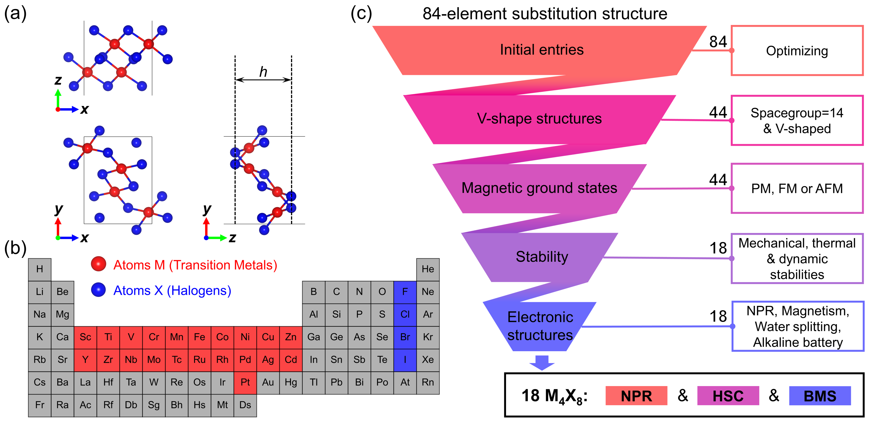
As illustrated in Figure 1(a), the primitive cell of the \ceM4X8 monolayer includes four M atoms (depicted as red spheres) and eight X atoms (depicted as blue spheres), forming a rectangular lattice. Each M atom is bonded to four X atoms, while each X atom is coordinated with two M atoms. From a side view, the \ceM4X8 monolayer exhibits a zigzag-shaped, V-like corrugated structure with a buckling height of . This arrangement lacks mirror symmetry but maintains centro-symmetry. The \ceM4X8 monolayer inherits the non-metallic shielding characteristics of traditional transition metal dichalcogenides (TMCs), such as the 1T and 2H phases, with metal M atoms situated in the central layer and non-metallic X atoms positioned in the outer layers.
Based on the \cePtI2 monolayer with (No.14) symmetry, we constructed 84 V-shaped corrugated monolayers by substituting Pt and I atoms with other elements of the periodic table. Figure 1(b) highlights the selected elements: M includes 21 transition metals (Sc-Zn, Y-Cd, and Pt), and X includes 4 halogens (F, Cl, Br, and I). Figure 1(c) illustrates the workflow of our high-throughput calculations. Among the 84 optimized \ceM4X8 monolayers, 40 structures either lost their corrugated configuration or failed to maintain symmetry, indicating that these structures are unsuitable for the V-shaped corrugated configuration. We focus on the remaining 44 monolayers, whose optimized structures retain the initial symmetry and potentially exhibit NPR characteristics. To further determine the magnetic ground states of these 44 structures, we considered not only paramagnetic and ferromagnetic states but also three types of antiferromagnetic (AFM) states, with specific spin arrangements detailed in Supplementary Figure S1. The calculations reveal that even combinations of the same metal element with different halogens can exhibit distinct magnetic ground states. For instance, \ceCr4Cl8 adopts an AFM state, while \ceCr4Br8 and \ceCr4I8 exhibit ferromagnetic states.
To evaluate the stability of the proposed materials, we firstly calculated the cohesive energy () of the \ceM4X8 structures to assess their thermal stability. The cohesive energy is defined as:
| (1) |
where , , and represent the energy of a single M atom, a single X atom, and the total energy of the \ceM4X8 unit cell, respectively. The quantities and denote the number of M and X atoms in the unit cell. The results show that the cohesive energies of all 44 structures are positive, indicating that these V-shaped materials exhibit high thermodynamic stability and are likely to be synthesizable. We found that the cohesive energy of \ceM4X8, formed by the same metal element and different halogens, decreases as the atomic number of the halogen increases. This may be attributed to the decrease in electro-negativity of the X atom, which enhances the ionic character of the metal-halogen bond and weakens its covalent character, leading to a more loosely packed structure of the compound and consequently a reduction in cohesive energy. The basic geometric parameters of these 44 structures, including lattice constants and , magnetic ground states, and cohesive energies, are summarized in Table S1 of the supplementary material.
To further verify the stability of the \ceM4X8 monolayers, we investigated their dynamic stability by calculating the phonon dispersion. Among the 44 structures, 22 were found to be dynamically stable (detailed results are provided in Figures S2 and S4). Notably, \ceNi4F8 and \ceAg4F8 exhibited minor negative frequencies near the point (-0.095 and -0.081 THz, respectively), a phenomenon commonly observed in various two-dimensional materials, which does not compromise their dynamic stability. In contrast, the remaining 22 structures with significant negative frequencies were considered dynamically unstable. Subsequently, the thermal stability of the remaining 22 \ceM4X8 monolayers was assessed via AIMD simulations. As shown in Figure S4, \ceRu4Br8, \ceRh4Cl8, \ceTc4Cl8, and \ceTc4Br8 underwent significant structural distortions at 300 K, indicating a lack of thermal stability. In contrast, the total energy fluctuations of the other 18 \ceM4X8 monolayers remained below 3 eV (Figure S3), and their structures remained stable during the simulations, suggesting good thermal stability. Finally, the mechanical stability of these 18 thermally stable structures was analyzed using the Born criteria ( and ),31 where denotes the elastic constants. Excitingly, the stability assessments reveal that 18 V-shaped \ceM4X8 monolayers exhibit excellent thermodynamic, dynamic, thermal, and mechanical stabilities, indicating significant potential for experimental synthesis.
3.2 Mechanical Properties
In the previous section, we examined the basic mechanical properties of 18 stable \ceM4X8 monolayers. Here, we further discuss their elastic mechanical properties related to elastic constants (, , , and ), such as Young’s modulus and Poisson’s ratio. Specifically, the angle-dependent Young’s modulus and Poisson’s ratio can be expressed as follows:32
| (2) |
| (3) |
where , .
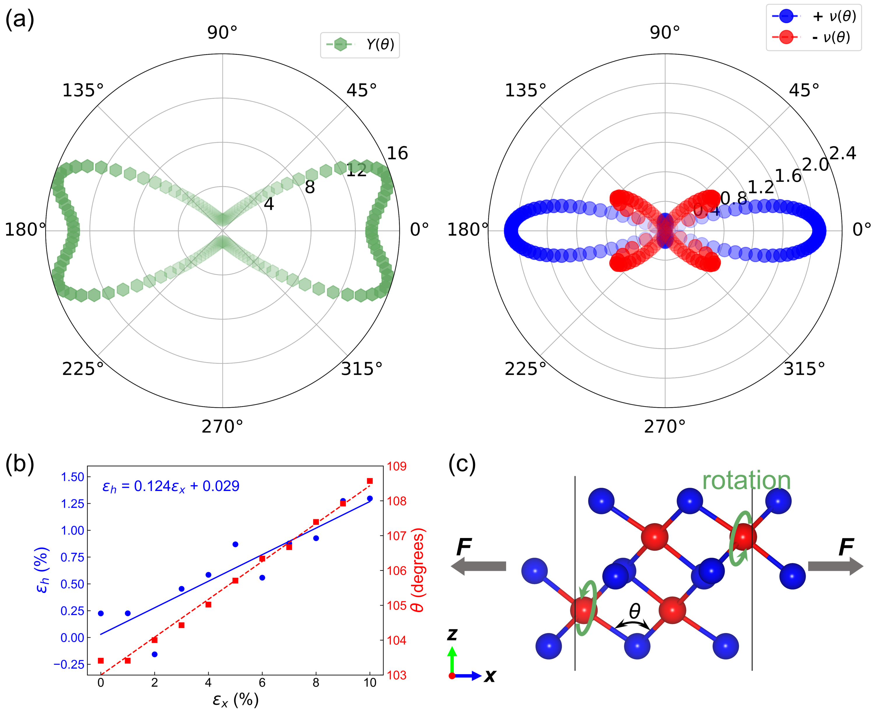
Based on the above equations, we present the variation of Young’s modulus () and Poisson’s ratio () with respect to angle () in Figure 2(a) (taking \cePd4I8 as an example). The results show that the monolayer \cePd4I8 exhibits NPR characteristics, with a maximum Young’s modulus of 15 N/m and a minimum negative Poisson’s ratio of -0.798, occurring at = 42°. Table 1 lists the relevant parameters of the mechanical properties for 18 \ceM4X8 monolayers, all of which exhibit relatively low in-plane Young’s modulus (less than 31 N/m) and significant anisotropy (see Figures S5 and S6). The highest in-plane Young’s modulus typically occurs along the -axis, which is also the direction with the maximum positive Poisson’s ratio. The Young’s modulus of these materials is significantly lower than that of graphene (340 N/m)33 and \ceMoS2 (330 N/m),34 indicating their promising potential for applications in flexible devices.
Notably, 8 \ceM4X8 monolayers exhibit NPR, with the lowest NPR values occurring in the direction between and , indicating their excellent mechanical properties such as dent resistance, high fracture toughness, and effective vibration or sound absorption capabilities. Specifically, the NPR values of \ceCu4Br8, \ceMo4Br8, and \ceAg4Br8 (-0.257, -0.068, and -0.151, respectively, as shown in Figure S6) are more negative than those of black phosphorus (-0.027)35 and -\ceSiS2 (-0.054)36, suggesting that these V-shaped monolayers demonstrate more pronounced responses as auxetic materials. Additionally, the V-shaped buckling structures also exhibit out-of-plane NPR characteristics, including \ceAg4Br8, \ceCu4Cl8, \ceCu4Br8, \ceMo4Br8, \ceNi4Cl8, \cePd4Br8, \cePd4I8, \cePt4Br8 and \cePt4I8. As illustrated in Figure 2(b), the strain degree of the buckling height () of the \cePd4I8 structure increases with tensile strain applied along the -direction (). Based on the linear fitting, the out-of-plane NPR of the \cePd4I8 structure is predicted to be -0.124. To explain the mechanism of out-of-plane NPR, Figure 2(c) illustrates the local structure. As can be seen, applying tensile strain along the -axis causes the lattice constant to increase, to decrease, and the bond angle to expand. This transformation induces a rotation of the \ceMX4 units within the unit cell, causing the two central \ceMX4 units to adopt a more vertical alignment. Consequently, the structural buckling height increases, leading to an out-of-plane negative expansion effect.
| System | |||||||
|---|---|---|---|---|---|---|---|
| \ceCr4Cl8 | 20.70 | 2.66 | 9.25 | 6.32 | 19.94 | 0.082 | |
| \ceCr4Br8 | 20.26 | 3.61 | 10.86 | 6.24 | 19.06 | 0.154 | |
| \ceCr4I8 | 18.38 | 3.04 | 6.02 | 5.49 | 16.85 | 0.004 | |
| \ceNi4F8 | 40.02 | 7.66 | 40.02 | 8.22 | 38.55 | 0.191 | |
| \ceNi4Cl8 | 31.68 | 2.69 | 9.52 | 6.16 | 30.91 | 0.085 | |
| \ceNi4Br8 | 26.19 | 3.14 | 5.62 | 5.74 | 24.43 | -0.033 | |
| \ceNi4I8 | 25.90 | 2.99 | 7.76 | 6.82 | 24.75 | 0.008 | |
| \ceCu4F8 | 31.28 | 5.82 | 7.43 | 6.30 | 26.72 | 0.073 | |
| \ceCu4Cl8 | 23.38 | 2.20 | 6.26 | 5.52 | 22.61 | 0.007 | |
| \ceCu4Br8 | 18.93 | 1.84 | 2.41 | 3.76 | 17.51 | -0.257 | |
| \ceMo4Br8 | 15.78 | 2.51 | 2.57 | 2.93 | 13.32 | -0.068 | |
| \ceMo4I8 | 16.11 | 2.46 | 5.14 | 4.74 | 14.93 | -0.004 | |
| \cePd4Br8 | 21.97 | 1.84 | 3.91 | 4.15 | 21.10 | -0.057 | |
| \cePd4I8 | 19.74 | 3.00 | 1.44 | 4.17 | 15.63 | -0.798 | |
| \ceAg4F8 | 18.97 | 2.72 | 3.63 | 2.55 | 16.93 | 0.137 | |
| \ceAg4Br8 | 12.22 | 3.19 | 4.38 | 2.83 | 9.90 | 0.187 | |
| \cePt4Br8 | 24.07 | 2.72 | 2.22 | 4.78 | 20.74 | -0.478 | |
| \cePt4I8 | 23.23 | 1.83 | 4.86 | 5.21 | 22.55 | -0.079 |
3.3 Electronic Properties
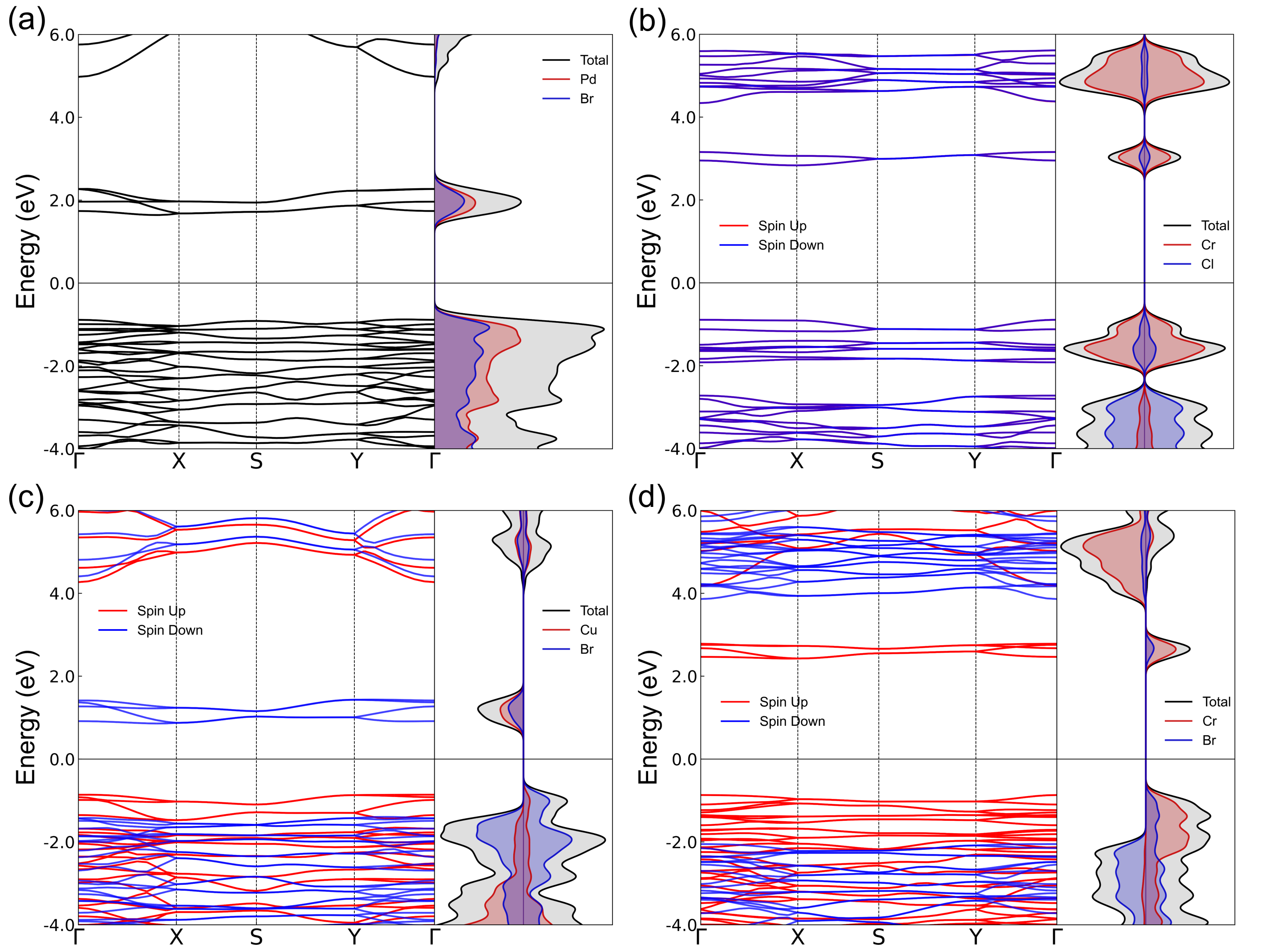
Considering the rich diversity of magnetic ground states exhibited by the V-shaped \ceM4X8 monolayers, we further investigated their electronic properties to expand their potential applications. The electronic band structures (including band gaps and types) and atomic projected density of states (PDOS) for 18 \ceM4X8 monolayers were calculated (see Table S2). Among these materials, \ceAg4Br8 exhibits metallic behavior, while the other 17 structures are semiconductors, all with indirect band gaps. Given that the PBE functional tends to underestimate band gaps, the HSE06 method was employed to obtain more reliable values. The corrected band types remained consistent with the PBE results, though the band gaps of the 17 semiconductors increased to varying extents, while \ceAg4Br8 retained its metallicity. We observed that for \ceM4X8 monolayers composed of the same metal atom but different halogen atoms, the band gap decreases as the atomic number of the halogen increases. The primary reason is probably differences in the atomic radii and electro-negativity of the halogen atoms, which result in variations in the bond lengths and charge distribution between the M and X atoms. Halogens with lower electronegativity (e.g., Iodine) exhibit weaker electron-attracting abilities, raising the energy of the valence band and consequently narrowing the band gap. Moreover, as shown in Table S1, for example, in the case of \ceNi4B8, the lattice constants and increase with the atomic number of the halogen. Larger lattice constants generally reduce the ionic character and bond strength of the metal-halogen bonds, resulting in lower transition energies for electrons between the valence and conduction bands, thereby decreasing the band gap.37, 38
Through the analysis of band structures and PDOS calculated using the HSE06 functional (as shown in Figure 3 and Table S2), we identified four typical semiconductor types: paramagnetic semiconductors, antiferromagnetic semiconductors, half-semiconductors (HSC),39, 40 and bipolar magnetic semiconductors (BMS),41, 42, 43, 44, 45 For all four categories, the valence band maximum (VBM) and conduction band minimum (CBM) are composed of contributions from the M and X atoms. Excitingly, among the ferromagnetic semiconductors, we identified 2 HSCs (\ceCr4Br8 and \ceCr4I8) and 5 BMSs (\ceCu4F8, \ceCu4Cl8, \ceCu4Br8, \ceMo4Br8, and \ceMo4I8). HSCs exhibit semiconducting behavior in one spin channel and semiconducting or insulating behavior in the other. The valence band and conduction band of HSCs are spin-split, with the VBM and CBM having the same spin direction. Due to the complete spin polarization of the VBM and CBM, HSCs can generate 100% spin-polarized electrons and holes under thermal or optical excitation, or simply through electric gating. Similarly to HSCs, BMSs also allow for electrical control of the spin orientation of charge carriers, a crucial feature for developing high-performance spintronic devices. However, unlike HSCs, the VBM and CBM in BMSs are fully spin-polarized in opposite spin directions. This unique property enables BMSs to control the spin direction of charge carriers by applying positive and negative gate voltages, while also adjusting their conductivity. Based on BMSs, various electrically controlled spintronic devices have been developed, such as bipolar field effect spin filters and field effect spin valves.46 These properties position \ceCr4Br8, \ceCr4I8, \ceCu4Br8, \ceCu4Cl8, \ceCu4F8, \ceMo4Br8, and \ceMo4I8 as promising candidates for advancing spintronic technology.
3.4 Water Splitting
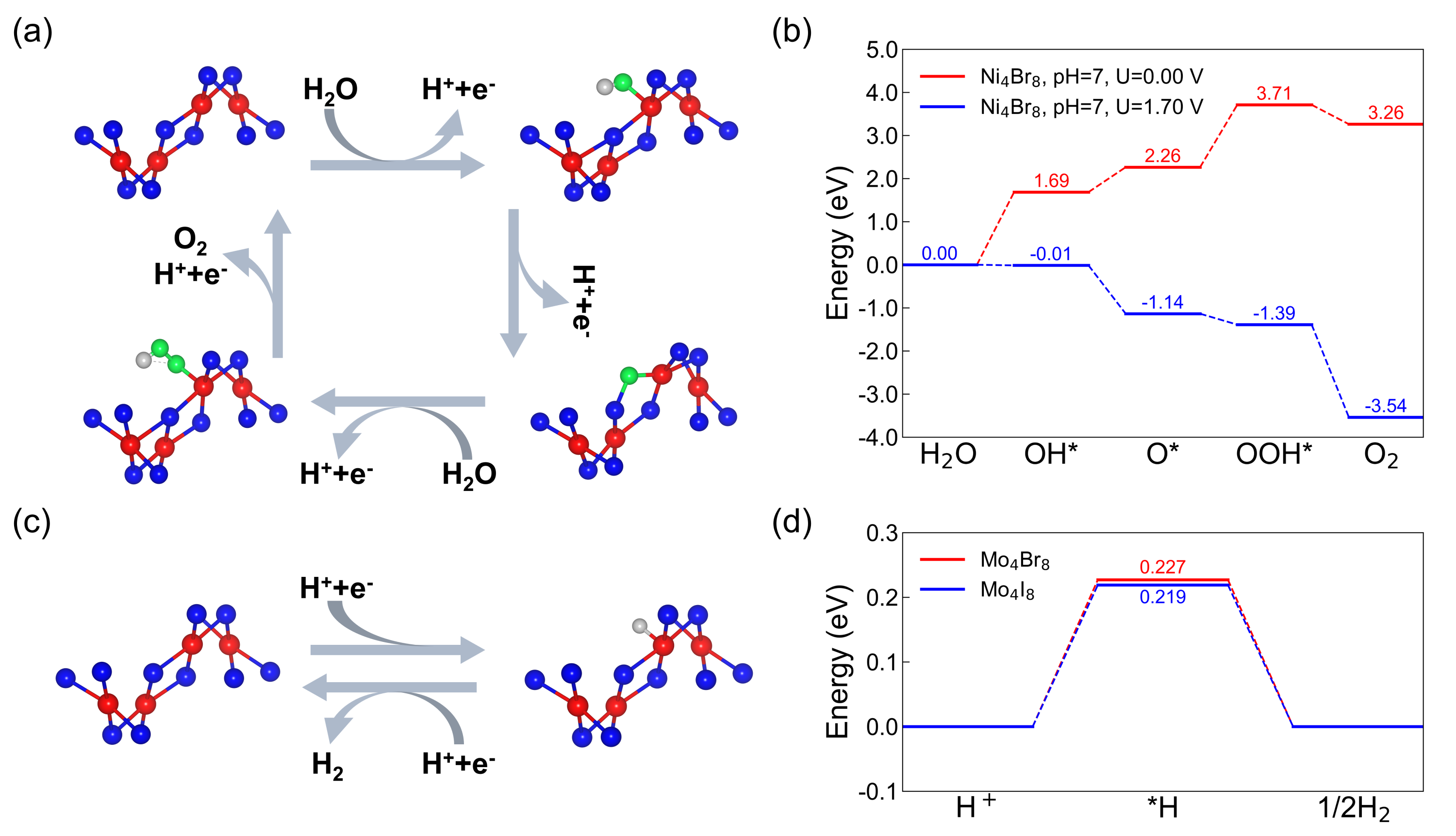
As shown in Figures 4(b) and (d), we calculated the OER performance of monolayer \ceNi4Br8 and the HER performance of \ceMo4Br8 and \ceMo4I8. Figures 4(a) and (c) illustrate the reaction steps and the lowest-energy intermediate structures (OH*, O*, OOH*, H*). For both OER and HER, the adsorption sites of intermediates are preferentially locate on metal atoms. For the OER, which follows a 4e- reaction pathway, the corresponding free energy (G) profiles are summarized in Figure 4(c). Initially, water adsorbs and transforms into OH*, with reaching a maximum of 1.68 eV. Subsequently, OH* is oxidized to O* by releasing H+ and an electron, with = 0.578 eV. The O* intermediate is then oxidized to OOH*, with = 1.447 eV. Finally, OOH* decomposes into oxygen, protons, and electrons, releasing 0.448 eV of energy. When an external potential (U = 1.70 V) is applied, all OER steps go downhill, indicating that water splitting on \ceNi4Br8 under these conditions can occur spontaneously. According to the formula provided in the supplementary information, the over-potential for \ceNi4Br8 under pH = 7 conditions is calculated to be 0.870 V. For the HER (Figure 4(d)), \ceMo4Br8 and \ceMo4I8 also demonstrate excellent performance. Under pH = 0 conditions, their values are 0.227 eV and 0.219 eV, respectively. These materials exhibit outstanding catalytic properties, suggesting that further optimization and exploration of their potential in practical applications could be highly promising.
3.5 Alkali Ions Migration
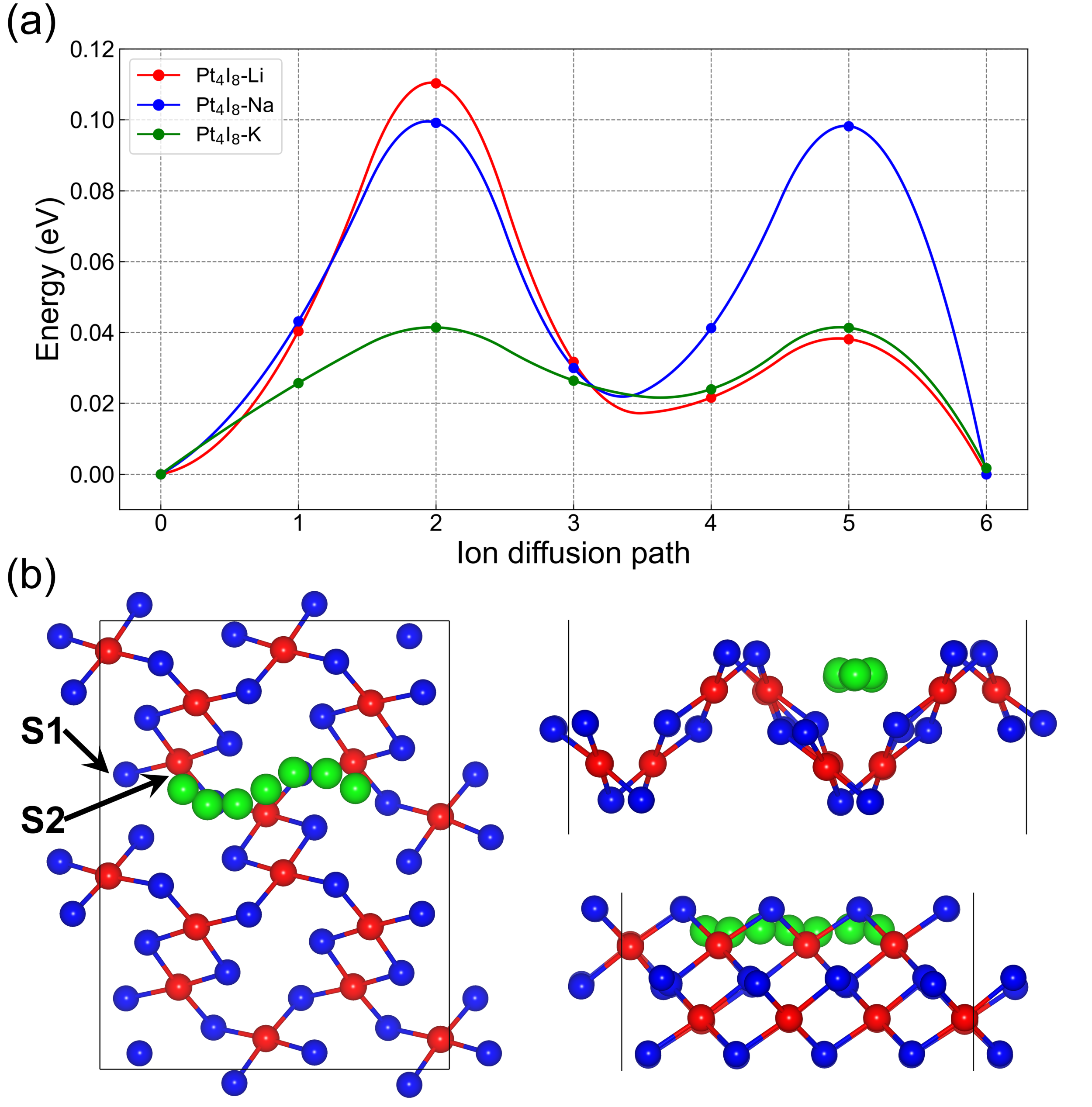
Building on structural analysis, we hypothesize that the grooves in the V-shaped structure facilitate alkali ion diffusion. Further studies revealed that the \ceM4X8 supercell forms linear channels along the -direction, which may promote the directional migration of alkali ions. To this end, we calculated the migration properties of a single Li, Na, and K ion in a 221 monolayer supercell. First, we investigated the adsorption behavior of Li, Na, and K atoms on \ceM4X8. Due to the spatial symmetry, only two possible adsorption sites, S1 and S2, were considered, as shown in Figure 5(b). The adsorption energy () was used to determine the most favorable adsorption site. The adsorption energy is calculated using the following formula:
| (4) |
where is the total energy of the \ceM4X8 monolayer with the Li/Na/K atom inserted, is the total energy of the pristine \ceM4X8 monolayer, and is the average energy of the Li/Na/K atom in its body-centered cubic (bcc) metallic phase. For the adsorption of Li/Na/K atoms on the \ceM4X8 monolayer, the at the S2 site is the lowest, with values of -0.834 eV/atom for Li, -0.890 eV/atom for Na, and -1.440 eV/atom for K. Then the CI-NEB calculations are then used to estimate the diffusion barriers. As expected ( see in Figure 5(a)), when ions migrate along the grooves, the diffusion energy barriers are very small. For Li ions, the diffusion energy barrier is 0.11 eV, which is smaller than that value of green phosphorus (0.14 eV)47 and \ceMoS2 (0.21 eV).48 For Na ions, the diffusion energy barrier is slightly lower than that of Li, decreasing to less than 0.10 eV, which is still lower than that of \ceMoS2 (0.28 eV)49 and penta-graphene (0.28 eV).50 Additionally, the diffusion energy barrier for K ions is only 0.04 eV, which is much lower than that value of \ceSi3C (0.18 eV),51 graphite (0.27 eV),52 and \ceTiC3 (0.19 eV),53 and significantly lower than that of Li and Na ions. Moreover, as seen from the corresponding ion diffusion paths in Figure 5(b), the migration of the K ion on \ceM4X8 has minimal impact on the material’s structure, demonstrating good structural stability, which is also true for Li and Na. In general, the low diffusion energy barriers indicate that \ceM4X8 is an excellent platform for ion migration and has potential for use in ion batteries.
4 Conclusions
Using DFT calculations, we performed a high-throughput analysis of 84 V-shaped corrugated \ceM4X8 monolayers. Among these, we identified 18 structures with thermodynamic, dynamic, mechanical, and thermal stability. Furthermore, we explored their potential applications in mechanical systems, spintronics, electrochemical catalysis, and alkali ion battery application. Our study indicates that 9 of the \ceM4X8 monolayers exhibit NPR characteristics. Notably, \cePd4I8 and \cePt4Br8 demonstrate outstanding NPR values, and their low Young’s modulus makes them promising candidates for flexible devices. The HSC properties of \ceCr4Br8 and \ceCr4I8, as well as the BMS characteristics of \ceCu4Br8, \ceCu4Cl8, \ceCu4F8, \ceMo4Br8, and \ceMo4I8, position these materials as promising candidates for spintronic devices. Additionally, \ceNi4Br8, \ceNi4Cl8, \ceMo4Br8, and \ceMo4I8 exhibit suitable band gaps and low over-potentials, indicating their potential for photocatalytic water splitting. Finally, the V-shaped crystal structure of monolayer \cePt4I8 provides an excellent platform for alkali ion migration, with low diffusion barrier. In all, this study paves the way for the discovery of additional 2D materials with multifunctional properties, further advancing the development of the field of low-dimensional electronics.
This work is supported by the National Natural Science Foundation of China (22203026, 22403024, 22203025, 22103020 and 12174080), the Fundamental Research Funds for the Central Universities (JZ2024HGTB0162) and the Anhui Provincial Natural Science Foundation (2308085QB52). The computation is performed on the HPC platform of Hefei University of Technology.
Computational methods details of OER and HER; Structural information of 18 stable \ceM4X8 and 24 unstable \ceM4X8 compounds; Schematic illustration of 4 different magnetic orders of \ceM4X8; Phonon spectra and 300K AIMD simulations of 18 stable \ceM4X8; Phonon spectra and 300K AIMD simulations for 4 dynamically stable but dynamically unstable \ceM4X8; Variation of Young’s modulus and Poisson’s ratio with angle for 18 stable \ceM4X8; PBE band gaps and HSE band gaps of 18 stable \ceM4X8 and their corresponding material types.
References
- Greaves et al. 2011 Greaves, G. N.; Greer, A. L.; Lakes, R. S.; Rouxel, T. Poisson’s ratio and modern materials. Nat. Mater. 2011, 10, 823–837
- Wu et al. 2018 Wu, D.; Wang, S.; Zhang, S.; Yuan, J.; Yang, B.; Chen, H. Highly negative Poisson’s ratio in a flexible two-dimensional tungsten carbide monolayer. Phys. Chem. Chem. Phys. 2018, 20, 18924–18930
- Wang et al. 2017 Wang, H.; Li, X.; Li, P.; Yang, J. -Phosphorene: a two dimensional material with a highly negative Poisson’s ratio. Nanoscale 2017, 9, 850–855
- Huang et al. 2017 Huang, B.; Clark, G.; Navarro-Moratalla, E.; Klein, D. R.; Cheng, R.; Seyler, K. L.; Zhong, D.; Schmidgall, E.; McGuire, M. A.; Cobden, D. H.; et al. Layer-dependent ferromagnetism in a van der Waals crystal down to the monolayer limit. Nature 2017, 546, 270–273
- Deng et al. 2018 Deng, Y.; Yu, Y.; Song, Y.; Zhang, J.; Wang, N. Z.; Sun, Z.; Yi, Y.; Wu, Y. Z.; Wu, S.; Zhu, J.; et al. Gate-tunable room-temperature ferromagnetism in two-dimensional Fe3GeTe2. Nature 2018, 563, 94–99
- Song et al. 2019 Song, T.; Fei, Z.; Yankowitz, M.; Lin, Z.; Jiang, Q.; Hwangbo, K.; Zhang, Q.; Sun, B.; Taniguchi, T.; Watanabe, K.; et al. Switching 2D magnetic states via pressure tuning of layer stacking. Nat. Mater. 2019, 18, 1298–1302
- Chen et al. 2023 Chen, B.; Hu, P.; Yang, F.; Hua, X.; Yang, F. F.; Zhu, F.; Sun, R.; Hao, K.; Wang, K.; Yin, Z. In situ porousized MoS2 nano islands enhance HER/OER bifunctional electrocatalysis. Small 2023, 19, 2207177
- Evarestov et al. 2017 Evarestov, R.; Kitaev, Y. E.; Porsev, V. Use of Wyckoff position splittings in the supercell model of crystals with point defects. J Appl Crystallogr 2017, 50, 893–900
- Shi et al. 2023 Shi, X.; Cheng, D.; Zhao, R.; Zhang, G.; Wu, S.; Zhen, S.; Zhao, Z.-J.; Gong, J. Accessing complex reconstructed material structures with hybrid global optimization accelerated via on-the-fly machine learning. Chem. Sci. 2023, 14, 8777–8784
- Ma et al. 2024 Ma, X.; Lan, C.; Lin, H.; Peng, Y.; Li, T.; Wang, J.; Azamat, J.; Liang, L. Designing desalination MXene membranes by machine learning and global optimization algorithm. J. Membr. Sci. 2024, 702, 122803
- Liu et al. 2018 Liu, C.; Li, W.; Fan, J.; Mai, Y. A brief review on the lead element substitution in perovskite solar cells. J. Energy Chem. 2018, 27, 1054–1066
- Huang et al. 2022 Huang, M.; Wang, S.; Zhang, T.; Chen, S. Searching for band-dispersive and defect-tolerant semiconductors from element substitution in topological materials. J. Am. Chem. Soc. 2022, 144, 4685–4694
- Zhang et al. 2015 Zhang, S.; Zhou, J.; Wang, Q.; Chen, X.; Kawazoe, Y.; Jena, P. Penta-graphene: A new carbon allotrope. Proc. Natl. Acad. Sci. U.S.A. 2015, 112, 2372–2377
- Liu et al. 2016 Liu, H.; Qin, G.; Lin, Y.; Hu, M. Disparate strain dependent thermal conductivity of two-dimensional penta-structures. Nano Lett. 2016, 16, 3831–3842
- Zhang et al. 2023 Zhang, J.; Zhang, W.; Zhang, L.; Du, G.; Yu, Y.; Xia, Q.; Wu, X.; Wang, Y.; Ji, W.; Qiao, J.; et al. Intralayer Negative Poisson’s Ratio in 2D Black Arsenic by Strain Engineering. Small Struct. 2023, 4, 2300178
- Zhang et al. 2020 Zhang, R.-Z.; Liu, J.; Zhang, Y.-Y.; Du, S.; Pantelides, S. T. Unusual anisotropic thermal expansion in multilayer SnSe leads to positive-to-negative crossover of Poisson’s ratio. Appl. Phys. Lett. 2020, 116, 083101
- Yu et al. 2017 Yu, L.; Yan, Q.; Ruzsinszky, A. Negative Poisson’s ratio in 1T-type crystalline two-dimensional transition metal dichalcogenides. Nat. Commun. 2017, 8, 15224
- Thiele et al. 1986 Thiele, G.; Weigl, W.; Wochner, H. Die Platiniodide PtI2 und Pt3I8. Z Anorg Allg Chem 1986, 539, 141–153
- Stoppiello et al. 2017 Stoppiello, C. T.; Biskupek, J.; Li, Z.; Rance, G. A.; Botos, A.; Fogarty, R. M.; Bourne, R. A.; Yuan, J.; Lovelock, K. R.; Thompson, P.; et al. A one-pot-one-reactant synthesis of platinum compounds at the nanoscale. Nanoscale 2017, 9, 14385–14394
- Shen et al. 2019 Shen, S.; Ma, Y.; Wang, H.; Huang, B.; Dai, Y. Single-layer PtI2: a multifunctional material with promising photocatalysis toward the oxygen evolution reaction and negative poisson’s ratio. ACS Appl. Mater. Interfaces 2019, 11, 31793–31798
- Kresse and Hafner 1993 Kresse, G.; Hafner, J. Ab initio molecular dynamics for open-shell transition metals. Phys. Rev. B 1993, 48, 13115
- Kresse and Hafner 1993 Kresse, G.; Hafner, J. Ab initio molecular dynamics for liquid metals. Phys. Rev. B 1993, 47, 558
- Kresse and Furthmüller 1996 Kresse, G.; Furthmüller, J. Efficiency of ab-initio total energy calculations for metals and semiconductors using a plane-wave basis set. Comput. Mater. Sci. 1996, 6, 15–50
- Kresse and Joubert 1999 Kresse, G.; Joubert, D. From ultrasoft pseudopotentials to the projector augmented-wave method. Phys. Rev. B 1999, 59, 1758
- Perdew et al. 1996 Perdew, J. P.; Burke, K.; Ernzerhof, M. Generalized gradient approximation made simple. Phys. Rev. Lett. 1996, 77, 3865
- Monkhorst and Pack 1976 Monkhorst, H. J.; Pack, J. D. Special points for Brillouin-zone integrations. Phys. Rev. B 1976, 13, 5188
- Heyd et al. 2003 Heyd, J.; Scuseria, G. E.; Ernzerhof, M. Hybrid functionals based on a screened Coulomb potential. J. Chem. Phys. 2003, 118, 8207–8215
- Togo and Tanaka 2015 Togo, A.; Tanaka, I. First principles phonon calculations in materials science. Scr. Mater. 2015, 108, 1–5
- Wang et al. 2023 Wang, H.; Li, T.; Liu, X.; Zhu, W.; Chen, Z.; Li, Z.; Yang, J. mech2d: An Efficient Tool for High-Throughput Calculation of Mechanical Properties for Two-Dimensional Materials. Molecules 2023, 28, 4337
- Henkelman et al. 2000 Henkelman, G.; Uberuaga, B. P.; Jónsson, H. A climbing image nudged elastic band method for finding saddle points and minimum energy paths. J. Chem. Phys. 2000, 113, 9901–9904
- Ding and Wang 2013 Ding, Y.; Wang, Y. Density functional theory study of the silicene-like SiX and XSi3 (X= B, C, N, Al, P) honeycomb lattices: the various buckled structures and versatile electronic properties. J. Phys. Chem. C 2013, 117, 18266–18278
- Cadelano et al. 2010 Cadelano, E.; Palla, P. L.; Giordano, S.; Colombo, L. Elastic properties of hydrogenated graphene. Phys. Rev. B 2010, 82, 235414
- Lee et al. 2008 Lee, C.; Wei, X.; Kysar, J. W.; Hone, J. Measurement of the elastic properties and intrinsic strength of monolayer graphene. Science 2008, 321, 385–388
- Castellanos-Gomez et al. 2012 Castellanos-Gomez, A.; Poot, M.; Steele, G. A.; van der Zant, H. S. J.; Agraït, N.; Rubio-Bollinger, G. Elastic Properties of Freely Suspended MoS2 Nanosheets. Adv. Mater. 2012, 24, 772–775
- Jiang and Park 2014 Jiang, J.-W.; Park, H. S. Negative poisson’s ratio in single-layer black phosphorus. Nat. Commun. 2014, 5, 4727
- Liu et al. 2023 Liu, Y.; Li, W.; Li, F.; Chen, Z. Computational discovery of diverse functionalities in two-dimensional square disulfide monolayers: auxetic behavior, high curie temperature ferromagnets, electrocatalysts, and photocatalysts. J. Mater. Chem. A. 2023, 11, 20254–20269
- Mosconi et al. 2016 Mosconi, E.; Umari, P.; De Angelis, F. Electronic and optical properties of MAPbX3 perovskites (X= I, Br, Cl): a unified DFT and GW theoretical analysis. Phys. Chem. Chem. Phys. 2016, 18, 27158–27164
- Chen et al. 2021 Chen, C.; Kuai, Y.; Li, X.; Hao, J.; Li, L.; Liu, Y.; Ma, X.; Wu, L.; Lu, P. Impact of halogen substitution on the electronic and optical properties of 2D lead-free hybrid perovskites. J. Phys. Chem. C 2021, 125, 15742–15750
- Li and Yang 2016 Li, X.; Yang, J. First-principles design of spintronics materials. Natl. Sci. Rev. 2016, 3, 365–381
- Kimura et al. 2003 Kimura, T.; Kawamoto, S.; Yamada, I.; Azuma, M.; Takano, M.; Tokura, Y. Magnetocapacitance effect in multiferroic BiMnO3. Phys. Rev. B 2003, 67, 180401
- Li et al. 2012 Li, X.; Wu, X.; Li, Z.; Yang, J.; Hou, J. G. Bipolar magnetic semiconductors: A new class of spintronics materials. Nanoscale 2012, 4, 5680–5685
- Li and Yang 2013 Li, X.; Yang, J. Bipolar magnetic materials for electrical manipulation of spin-polarization orientation. Phys. Chem. Chem. Phys. 2013, 15, 15793–15801
- Yuan et al. 2013 Yuan, L.; Li, Z.; Yang, J. Hydrogenated bilayer wurtzite SiC nanofilms: a two-dimensional bipolar magnetic semiconductor material. Phys. Chem. Chem. Phys. 2013, 15, 497–503
- Chen et al. 2023 Chen, J.; Wang, X.; An, Y.; Gong, S.-J. Recent progress in 2D bipolar magnetic semiconductors. J. Phys. Condens. Matter 2023, 36, 083001
- Li et al. 2022 Li, J.; Li, X.; Yang, J. A review of bipolar magnetic semiconductors from theoretical aspects. Fundam. Res. 2022, 2, 511–521
- Li et al. 2023 Li, Y.; Deng, J.; Zhang, Y.-F.; Jin, X.; Dong, W.-H.; Sun, J.-T.; Pan, J.; Du, S. Nonvolatile electrical control of spin polarization in the 2D bipolar magnetic semiconductor VSeF. npj Comput. Mater. 2023, 9, 50
- Wang et al. 2022 Wang, H.; Liu, C.; Cao, Y.; Liu, S.; Zhang, B.; Hu, Z.; Sun, J. Two-dimensional layered green phosphorus as an anode material for Li-ion batteries. ACS Appl. Energy Mater. 2022, 5, 2184–2191
- Li et al. 2012 Li, Y.; Wu, D.; Zhou, Z.; Cabrera, C. R.; Chen, Z. Enhanced Li adsorption and diffusion on MoS2 zigzag nanoribbons by edge effects: a computational study. J. Phys. Chem. Lett. 2012, 3, 2221–2227
- Mortazavi et al. 2014 Mortazavi, M.; Wang, C.; Deng, J.; Shenoy, V. B.; Medhekar, N. V. Ab initio characterization of layered MoS2 as anode for sodium-ion batteries. J. Power Sources 2014, 268, 279–286
- Xiao et al. 2016 Xiao, B.; Li, Y.-c.; Yu, X.-f.; Cheng, J.-b. Penta-graphene: a promising anode material as the Li/Na-ion battery with both extremely high theoretical capacity and fast charge/discharge rate. ACS Appl. Mater. Interfaces 2016, 8, 35342–35352
- Wang and Li 2020 Wang, Y.; Li, Y. Ab initio prediction of two-dimensional Si3C enabling high specific capacity as an anode material for Li/Na/K-ion batteries. J. Mater. Chem. A 2020, 8, 4274–4282
- Xu et al. 2016 Xu, Z.; Lv, X.; Chen, J.; Jiang, L.; Lai, Y.; Li, J. Dispersion-corrected DFT investigation on defect chemistry and potassium migration in potassium-graphite intercalation compounds for potassium ion batteries anode materials. Carbon 2016, 107, 885–894
- Fatima and Park 2024 Fatima, S. A.; Park, J. Two-dimensional carbon rich titanium carbide (TiC3) as a high-capacity anode for potassium ion battery. Appl. Surf. Sci. 2024, 659, 159879