Control of ferroelectric domain wall dynamics by point defects: Insights from ab initio based simulations
Abstract
The control of ferroelectric domain walls and their dynamics on the nanoscale becomes increasingly important for advanced nanoelectronics and novel computing schemes. One common approach to tackle this challenge is the pinning of walls by point defects. The fundamental understanding on how different defects influence the wall dynamics is, however, incomplete. In particular, the important class of defect dipoles in acceptor-doped ferroelectrics is currently underrepresented in theoretical work. In this study, we combine molecular dynamics simulations based on an ab initio-derived effective Hamiltonian and methods from materials informatics, and analyze the impact of these defects on the motion of 180∘ domain walls in tetragonal BaTiO3. We show how these defects can act as local pinning centers and restoring forces on the domain structure. Furthermore, we reveal how walls can flow around sparse defects by nucleation and growth of dipole clusters, and how pinning, roughening and bending of walls depend on the defect distribution. Surprisingly, the interaction between acceptor dopants and walls is short-ranged. We show that the limiting factor for the nucleation processes underlying wall motion is the defect-free area in front of the wall.
I Introduction
The success of ferroelectric materials in a plethora of applications depends on reversible polarization () switching by electrical fields (), either at the macroscopic level or at the nanoscale. [1, 2] Particularly the latter is related to domain walls (DWs), i.e. the interfaces that separate domains with different polarization directions. These nanoscale objects move in applied fields and offer tremendous potential for miniaturization and realization of advanced nanoelectronics and novel computing schemes, such as neuromorphic computing. [3, 4, 5] Moreover, the motion of these walls or wall segments contributes significantly to the macroscopic dielectric [6, 7] and piezoelectric [8, 6, 9] properties of ferroelectric materials. The full potential of DWs can however only be tapped by their macroscopic and nanoscale control.
Due to their importance, ferroelectric DWs and their dynamics were already studied by Merz in the early 1950s. It was shown that the DW velocity increases with temperature () and field strength () proportional to . [10] Furthermore, it was reported early that ferroelectric DWs are Ising-type and atomically sharp.[2] In recent years, these walls have been revisited and it is now consensus that wall motion is indeed a thermally activated process even in defect-free materials, as the walls are pinned by the underlying lattice.[11, 12, 13, 14, 15, 16, 17] Microscopic simulations revealed that wall motion is initiated by the nucleation and growth of two-dimensional (2D) clusters in front of the wall [18, 19, 20, 12] and is thus governed by local switching events rather than the macroscopic momentum of the walls. The classical interpretation of walls and their motion has been challenged by reports on Bloch and Néel-like polarization rotation [21, 22, 23, 24] and complex multi-step switching on DWs.[25, 26]
Probably the most successful approach to controlling the properties and motion of the DW is by doping and defect engineering.[27, 28, 29] On the one hand, defects may act as nucleation centers, lowering the coercive field and increasing the velocities of the walls.[13, 30] Also pinching of hysteresis by defects has been reported. [31, 32, 33] On the other hand, pinning by defects can slow down the wall dynamics and increase the coercive field for macroscopic switching, so-called hardening.[34] Defects non-commensurate with the lattice have been related to successive pinning and depinning of walls at a disordered energy landscape and thus to jerky or intermittent wall motion.[35, 36, 37, 38, 6, 39] It has been reported that the curvature of the DWs under field-driven motion results from the competition between the local pinning potentials that resist simple sliding and the elastic energy of these propagating interfaces, which tends to maintain flat walls.[40, 41] Furthermore, it has been reported that DWs respond mechanically to distortions and fields like a membrane.[42]
[abs]
So far, the understanding of the underlying defect-wall coupling is incomplete and various mechanisms have been predicted. Pinning of walls or their segments has been reported for point defects,[43] vacancies, impurities, dislocations,[44] Zr-rich regions in Pb(ZrxTi1-x)O3 [35] or SrTiO3-inclusions in BaTiO3,[45] and at grain boundaries. [46, 47] Often not even the types of existing defects in the used samples are known. It is furthermore challenging to access nanoscale subsurface defects and domain structures with sufficient time resolution experimentally. Instead, atomistic simulations[48, 49] and statistical models,[39] give access to the fundamental coupling mechanism. Typically, these distinguish random bond and random field defects.[50] Random bond defects, such as substituents with the same valency, can couple with walls via strain, the local modification of the ferroelectric instability, or the energy barrier for switching, but do not break the local symmetry. For vacancies, large concentrations (%) have been studied by density functional theory (DFT) predicting that these pin DWs.[48, 49] In contrast to that, molecular dynamics (MD) simulations at finite temperatures, have revealed that single vacancies can actually promote domain nucleation and switching.[13] An even larger influence on walls can be expected by random field defects which favor one polarization direction, act as local bias fields, and break the local symmetry.[6, 34] Surprisingly, their coupling to DWs on the microscopic scale is underrepresented in literature. This leads to important gaps in knowledge hindering the nanoscale control of DWs.
In this work we focus on one important subclass of local-field type pinning centers: Charge-neutral acceptor dopant ()–oxygen vacancy () complexes - in the prototypical ferroelectric material BaTiO3 which are aligned with the surrounding polarization after aging and can only be reoriented through orders of magnitude slower ion migration. These defects have been reported to act as local restoring forces on the polarization [34, 33] and thereby improving macroscopic functional properties, e.g. reversible dielectric, piezoelectric, and electrocaloric responses.[51, 52, 53, 33] To the best of our knowledge, so far only one MD study on the interaction between charged DWs and defect dipoles in this material has been published.[23] They found that 1 % oxygen vacancies can slow down the DW motion through the formation of defect dipoles, but these defects have a very localized effect on the surrounding dynamics and may not be able to pin a moving DW due to longer relaxation times.
Here, instead of charged DWs, we focus on energetically favorable, charge-neutral tetragonal 180∘ DWs. Using ab initio derived molecular dynamics simulations, we analyze the field-induced wall motion for different defect distributions in a broad concentration range (0.025 – 2 % defects). We show that the coupling between walls and these defects is short-ranged and thus the defect distribution and particularly the defect-free area in front of the wall is decisive for the wall motion.
II Methods
We perform molecular dynamics simulations using the feram simulator[54], which is based on the effective Hamiltonian approach by Rabe, Zhong and Vanderbilt [55, 56]:
| (1) |
where all degrees of freedom are coarse-grained to and , the soft mode and acoustic displacement vectors in each unit cell (u.c.), respectively, see Fig. 1 (a)–(b). These local soft modes are related to the local polarization as , with and being the effective Born charge of the unit cell and its volume. The potential energy terms are , the self-energy of the local soft modes, and , their long-range and short-range interactions, and , the elastic energies from homogeneous and inhomogeneous strain, with being the six components of the homogeneous strain tensor in Voigt notation (, ), and , which is the coupling between the local soft modes and homogeneous and inhomogeneous strain. The last term couples the local soft modes to an external electric field. As homogenous strain and are internally optimized, only the kinetic energy of the local soft modes, with an effective mass , is explicitly included in the simulations. Together with the ab initio parameterization from Ref. 54, this model can successfully describe the full temperature-phase diagram of BaTiO3. However, it underestimates experimental transition temperatures and the tetragonal phase is (meta-)stable between 180 K and 275 K (140 K – 295 K). This has been related to the underlying DFT data,[54] missing anharmonicities (e.g., thermal expansion), and missing higher-energy phonon modes. [57, 58]
Without loss of generality, we align the tetragonal axes along and thus set the components of the time-averaged local polarization to and . We then approximate -V complexes by frozen-in defect dipoles (). The strength of these dipoles is adjusted by supplementary DFT calculations for the transition metal ions : Cu+2, Mn+2, and Fe+2 using the VASP code [59] together with PBEsol potentials and Hubbard corrections of 6.52, 7.2 and 6.8 eV, respectively. The used supercells with one defect dipole each correspond to a defect concentration of approximately 4 %. To reduce finite-size effects, the simulation cell is constrained to the tetragonal structure of pristine BaTiO3, while atomic positions are relaxed with a force threshold of 0.01 eV/Å using a plane-wave cutoff energy of 520 eV and k-point sampling of . Using this approach, we find defect strengths of 29.6 (24.9), 29.1 (25.1), and 29.5 (25.3) C/cm2 for Cu+2, Mn+2, and Fe+2 for parallel (antiparallel) alignment of defect dipoles and surrounding polarization and 30.9 C/cm2 for pristine BaTiO3. Thus, antiparallel defects reduced the local polarization roughly by a factor of 0.95 (0.81). For simplicity, we fix the defect dipole to 24.7 C/cm2, i.e. which is a factor of 0.8 smaller than in the ferroelectric phase.111Note that the DFT informed defect strength is an approximation which does not include the change of this ratio with temperature. Close to the transition temperature, e.g. at 280 K the ratio of the chosen defect strength and the polarization of the pristine material increases to 0.9. As illustrated in Fig. 1 (d)–(e), we only consider defect dipoles initially aligned with the polarization direction of the surrounding domains, i.e. along in domains or along in domains.
For our large-scale MD simulations, we use a system size of u.c. of BaTiO3 together with periodic boundary conditions and the Nosé-Poincaré thermostat with a timestep of 1 fs. If not stated otherwise, we discuss results for DWs at 260 K. We initialize and thermalize dipoles in equidistant domains with and , separated by tetragonal 180∘ DWs normal to , see Fig. 1, by applying local fields kV/cm for 30 ps. After further equilibration without field, we instantaneously apply a homogenous field kV/cm for 100 ps. This field strength is sufficient to depin DWs from the lattice in the temperature range of interest (240–280 K). Note that it is expected that experimental field strengths are overestimated in simulations on idealized materials and without explicit treatment of the electrodes.[61, 62]
In order to characterize the DWs, we identify the center of the walls () with u.c. resolution by the sign change of , the -component of the local polarization, after taking moving averages over unit cells along the -direction. This technique is similar to box-blur in image processing. As proven for one example, the results are converged with respect to the chosen convolution kernel size of 11 u.c. The mean square wall roughness is given as
| (2) |
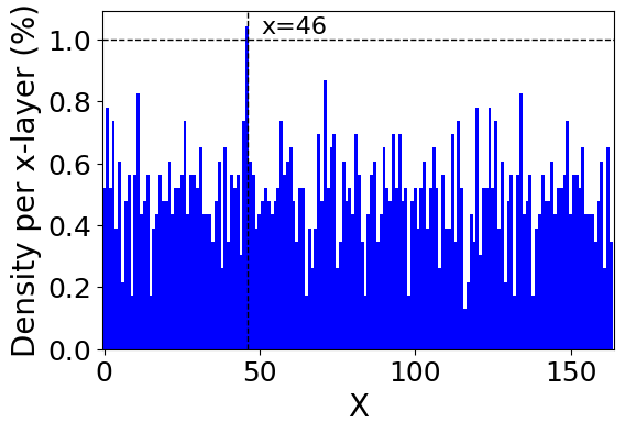
with the sum running over all u.c. segments on -planes and being the mean value of . As the wall roughness is not a measure for the wall width, we supplementary determine the mean widths () of the walls based on the mean polarization per -layer with
| (3) |
where , , and are fit parameters. Note that this equation can only estimate the wall width for flat walls, while is overestimated in case of wall bending.
To estimate critical dilations of nuclei on the moving wall, we furthermore analyze the time evolution of dipole clusters switching from to on separate -planes (slices) in 9 independent simulations in the time interval ps.
[abs]
We define a cluster as a connected region of unit cells on one plane and record statistics over the evolution of clusters on different planes. Cluster analysis is performed through a wrapper around the labeling capabilities implemented in skicit-image. [64] To distinguish thermal fluctuations and nucleating clusters, we filter out all clusters which exist for only one timestep (1 ps). We then extract the critical in-plane dilations of nuclei, and their standard deviations. Details of the implementation and a description of procedure including outlier detection can be found in Refs. 65, 26. The only change with respect to the provided reference is an adaption to tetragonal symmetry.
III Results & Discussion
III.1 Domain wall motion in the pristine material
To understand how defects modify DWs and their motion, the field-response of the pristine material (no defects) is needed as reference. Without an applied field, the mean DW roughness (width) between 240 K and 280 K is 0.8 – 1.2 u.c. (0.6 – 1 u.c.), i.e. less than 0.5 nm, in agreement with predictions from literature. [66, 15] There is no driving force for wall motion and temporary broadening or shifting of walls are rare events for the given temperature range.[18, 12] An external field , parallel to the domain, acts as a driving force for the growth of this domain. As discussed in Refs. 19, 20, one can distinguish three field regimes: (i) Pinning by the lattice: The energy barrier to shift the walls from BaO planes to TiO2 planes is large compared to the activation energy related to the applied field. The motion of the wall is a rare event and the macroscopic ferroelectric polarization does not change with time (no switching). (ii) Switching by thermally activated DW propagation along -direction is activated by kV/cm. With increasing field strength, the velocity of the walls and non-equilibrium effects after the fast field application, increase. The latter induces temporary sign change of dipoles in the blue domain and thereby the boost of the initial wall velocity. This is the precursor for regime (iii), the additional homogeneous nucleation in the antiparallel domain and fast switching by 3D growth of these nuclei which appear for more than about 400 kV/cm.
In the remainder of the paper we focus on field-regime (ii), the thermally activated wall motion in kV/cm. In agreement to predictions by atomistic and coarse-grained simulations in Refs. 12, 18, this motion starts with enhanced dipole fluctuations on the wall and the nucleation of 2D clusters of dipoles aligned with the field. Our cluster analysis yields lower bounds for the critical size of these nuclei of about and u.c. along the polarization direction () and perpendicular to it (). After rapid expansion along , 2D stripe domains are formed on the walls, see Fig. 2 (a), which grow and merge by slower sideway motion along until the whole plane has switched. With time, the walls move through the material by this thermally activated process, see Fig. 2 (b). Thereby, the probability to nucleate a 2D cluster in front of the walls is constant on all -planes and in different simulation runs. The -interface is thus no longer flat, different segments of the wall have propagated more than others and the positions of the wall center () deviate up to 3.4 u.c, Fig. 2 (b).
The anisotropies of the critical cluster dilations and the cluster growth are related to the large additional energy penalty to form charged interfaces (depolarization) along the polarization direction . On the one hand, interfaces along and are charge-neutral and low in energy. On the other hand, interfaces along are charged and the depolarization fields induce large energy penalties, see Fig. 2 (c)–(d).[20, 12]
[abs]
In the steady-state, the velocity of the wall motion increases from 0.4 Å/ps at 240 K by factors of approximately 2.5 and 4 if going to 260 K and 280 K, as shown in Fig. 3 (b).222Note that the polarization in the domain and the wall velocity increase and decrease with time. While the change of is negligible at low temperatures, it reaches 5 % and 14 % at 260 K and 280 K. Note that at 280 K we can only monitor the walls for 60 ps. Afterwards they have crossed the simulation cell and annihilated the domain. For this temperature, we furthermore observe a non-equilibrium boost of the initial velocity already for this moderate field strength as initially about 3.5 % dipoles in the center of the negative domain are aligned with the field direction. With time these dipoles switch back until the steady state (about 2.4 % in the negative domain) is reached at around 40 ps. The fact that we find non-equilibrium switching at the moderate field strength is related to enhanced thermal fluctuations and reduced energy barriers for polarization switching close to the cubic to tetragonal phase transition of our model. Well in the tetragonal phase, the energy barrier for initial switching is higher and the steady state of the wall motion is already reached within the first 10 ps. The mean roughness of the walls is only about 1 u.c. and does not change significantly either with temperature or time, or between independent samples, see Fig. 3 (c).
In summary, DW motion in the pristine material follows the nucleation and growth of 2D clusters, which form at all points of the DW with equal probability. The velocity of this process is sensitive to temperature and field strength, while the DW roughness is less sensitive to these parameters.
III.2 Defect dipoles and wall motion: Random distribution
How do randomly distributed defect dipoles aligned with the initial domain structure, see Fig. 1 (d), affect the wall motion?
[abs]
As defect dipoles do not switch by thermal fluctuations or the applied field, one may expect that they induce local bias fields and pin the walls. To test this hypothesis, we analyze the wall properties for different defect concentrations, see Fig. 4. Indeed the mean wall velocity decreases systematically with defect concentration, i.e. by about 5 % and 50 % for 0.5 % and 1 % defects, and the critical density for full pinning is below 2 % defects, see Fig. 4 (b). Furthermore, already 0.5 % defects suppress the initial boost of the DW velocity at 280 K, cf. appendix Fig. 10. For a given defect concentration, the wall velocity furthermore decreases with the strength of the defects, e.g. to Å/ps for () and 1% defects, cf. appendix Fig. 11, and a smaller critical concentration for pinning can be expected.
Not only the DWs but also the polarization in the domains is modified by the defect dipoles. For the DFT-informed defect strength corresponding to , the mean polarization in both domains is reduced by 0.7 %, 1.2 % and 2.1 % for 0.5, 1 and 2 % defects. If defects and free dipoles are locally antiparallel to each other after wall motion, the local polarization is reduced further, e.g. by 13 % for 1 % defects. Stronger defects, e.g. =0.15 Å corresponding to , enhance the initial polarization by about 1 %. Macroscopically, the defects distributed in 3D space thus indeed act on the system as bias fields and one may expect an enhanced coercive field experimentally. As the critical density for full pinning of 2 % is the lower bound of the defect concentration used in many atomistic studies, these predict wall pinning by acceptor dopants. For slightly smaller defect concentrations, however, already a moderate field is sufficient to depin the walls, cf. Fig. 5 (a). Fully in line with the interpretation of defect-induced bias fields, 1 % randomly distributed defects also restore the initial wall position and shape once the external field is removed, see Fig. 5. Even though some wall segments have moved by more than 10 u.c. in the field (a), the wall relaxes back to its initial position in about 40 ps (b). Our simulations can thus prove the predictions in Ref. 33 that point defects may act as a restoring force on the domain structure and are thus beneficial for large reversible functional responses.
[abs]
In addition to these macroscopic changes, the defects also induce time-dependent variations of wall velocities and roughening, see Fig. 4 (b)–(c). For the intermediate concentration of 1 %, the mean wall roughness even increases systematically with time and after 100 ps it is twice the value of the pristine material. Furthermore, wall velocity and roughening vary between statistically independent simulations (colored backgrounds) with maximal deviations of up to 47 % and 15 %, see shaded areas in Fig. 4. Even larger deviations have to be expected between different random defect distributions, particularly if of different homogeneity.
[abs]
These observations are a consequence of local pinning and sequential depinning of wall segments at defect-rich regions. For low defect concentrations, the defect configuration in most layers only interacts weakly with the moving wall. Particularly there is no tendency for wall pinning at separate defects. Instead, the wall segments flow around these defects. The main influence of 0.5 % defects is thus to reduce the local probabilities for nucleation and growth of new clusters and the forward motion of parts of the wall. A random distribution of 1 % defects, however, temporarily pins a significant fraction of wall segments. As the pinned segments for 1 % defects are at different positions on different -layers, the roughening increases with time and is related to the bending of the wall, see Fig. 5 (a). The velocity of the wall reaches a steady state as soon as the fraction of newly pinned and successively depinned segments balances for a sufficiently homogeneous distribution of defects. Due to variations of the local defect density, also the wall in the material with 0.5 % defects reaches a plane with 1 % defects at about 25 ps (see appendix Fig. 12) where a large fraction of segments is temporarily pinned. Therefore, the mean wall velocity shows a local minimum and the wall roughness is enhanced for about 20 ps, see Fig. 4. With time, the whole wall is depinned from the corresponding plane and initial wall roughness and velocity are restored while the wall passes layers with lower defect concentrations. In case of 2 % defects, some segments can penetrate defect-poor regions in the first 10 ps. The average wall position moves by 1 u.c and the roughness increases by about 18 %. Afterwards the local defect density and the defect distribution in -planes do not allow any further penetration of wall segments.
In summary, homogeneously distributed defect dipoles indeed induce internal bias fields, which act on the macroscopic field response as if the applied field had been reduced and which restore the initial domain structure. On the nanoscale, however, it depends on the local density and distribution of defects which wall segments are pinned and whether this pinning can persist with wall roughening and slowing down of the wall motion, or whether the walls can flow around separate defects.
III.3 Domain wall motion and defect plane
To gain a full microscopic understanding of the underlying local pinning and depinning processes, we turn to a defect distribution with different symmetry: A defect-rich plane (2D defect distribution) with defects is added in front of the wall, see Fig 1 (e). We answer the following questions: How long-ranged is the interaction between walls and defects? How do the defects pin and bend the wall? What is the local critical defect density to pin a wall?
Wall properties for different temperatures are compared in Fig. 6 (a)–(c). On the one hand, the chosen concentration of 3.5 % is locally above the critical concentration for pinning found for 3D distribution in the last section. On the other hand, it corresponds to a mean concentration of less than 0.025 % defects in the whole system and long-range bias fields can thus be ruled out. For all temperatures, these defects do not influence the wall before it crosses their plane, see time-evolution before the vertical dotted lines. Particularly there is no long-range interaction. For example at 240 K, the remaining distance between DW center and defect plane at 100 ps is only 1 u.c. Even for this distance, the mean wall velocity is identical to the pristine material. The same holds true for all tested defect concentrations, i.e. even planes with 7 % defects do not show long-range coupling with the walls moving towards it, see Fig. 6 (e)–(g). This short-range nature of the interaction is related to the small correlation of dipoles perpendicular to the polarization direction (cf. appendix Fig. 15). Only nearest neighbor dipoles are weakly correlated. Analogously, also sparse defects only couple to the polarization locally and along the polarization direction.
After the wall hits the defect plane, one can distinguish two time intervals of the wall–defect interaction for 3.5 % defects: (i) pinning of wall segments which reduces the mean velocity of the wall and increases the roughness, as discussed below, and (ii) sequential depinning of these wall segments which restores initial shape, roughness, and velocity. During this process, the speed of the wall may temporarily overshoot. At 280 K, the DWs cross the defect plane at about 10 ps and reach their maximal roughness about 20 ps later. Afterwards the time interval (ii) lasts until the end of the simulation. These processes are slower at 260 K as wall motion and depinning are induced by thermal fluctuations. At this temperature, the wall hits the defect plane at approximately 30 ps, the maximal roughness is reached at about 80 ps and interval (ii) is not yet completed after 100 ps. Qualitatively the same trends are observed for defect concentrations up to 4 %, see Fig. 6 (e)–(g). With the defect concentration, the time interval (i) and the slowing-down of the wall increase systematically. The maximal roughness is thus reached at 60 ps, 80 ps, or after 100 ps for 2 %, 3.5 %, or 4 % defects while the minimal velocity at 50 ps is only 49 %, 11 %, or 4.5 % of whose of the pristine material. For intermediate defect concentrations, particularly for 4 %, the DW velocity is furthermore very sensitive to the defect distribution, cf. dotted and dashed lines, and for more than 5 % defects, both tested configurations fully pin the wall without sizeable changes of DW roughness. Note that this local defect concentration corresponds to an average number of 0.03 % defects in the chosen simulation cell.
For simplicity, we restrict the following detailed analysis to 3.5 % defects and 260 K. Figure 6 (d) shows the underlying time-evolution of , the lines of averaged wall center positions over . Analogous to the defect-free material, the walls are initially rather flat and move with constant macroscopic velocity but host the nucleation of 2D clusters. At 30 ps (purple-red line) after the wall has hit the defect plane, the local probability for nucleation and growth in a large part of this plane is strongly reduced, and the wall velocity temporarily drops. At the next shown snapshot, one cluster (red) has penetrated the defect plane at the periodic boundary (spanning from about to the next periodic image, ) and has grown down and up to and at 90 ps. During this time, no other nucleus penetrates the defect plane, and while the cluster grows along by 14 u.c., the wall segments around are pinned. In turn the wall is bending and thus its roughness increases to 3 u.c. Local thermal fluctuations and the local wall width are however not significantly modified. Finally, after 100 ps, the wall is fully depinned from the defect plane, and the wall has started to flatten again with a maximal variation of of 11 u.c. Within longer simulations, the steady state of the moving flat wall was finally restored. Qualitatively the same trends are found for defect planes with 2–4 % defects.
[abs]
The underlying mechanisms for pinning and depinning are illustrated in Fig. 7. As defects cannot be switched, they cannot be part of a nucleus. Between dense defects, local dipole fluctuations are possible. However, appearing clusters do not reach their critical size and vanish again, see blue arrow in the upper part of Fig. 7 (a). Instead, clusters nucleate and move through large enough defect-free areas as shown in the lower part of the sketch, while the rest of the wall is pinned. This pinning of wall segments increases the wall area in the system as two additional walls parallel to start to grow, see red arrows in Fig. 7. These new interfaces share the properties of the walls along by symmetry, i.e. they are charge-neutral, degenerate and low energy, and face the same energy barrier for motion (TiO2 planes) as well as the same driving force (the field favoring domains). Note that the sharp corners of the nuclei shown in the sketch are potentially high in energy. Instead, the wall is locally bending and parts of it are no longer along a -type direction, see Fig. 6 (d).
The applied field induces the shift of wall segments along (-walls) and (-walls) with equal probability. Therefore, the pinned segment shrinks along and the total wall velocity along increases due to the additional increase of switched dipoles behind the front of the wall. Therefore, the velocity can temporarily exceed that of the pristine material as shown in Fig. 6 (f). At the same time, the increase in energy with the increasing wall area is minor and no slowing down of the depinned wall segments becomes visible with the chosen resolution. For example, the velocity of the wall for the segments – u.c. is identical to whose of the pristine material. By the combined wall growth along and the wall can also flow around the defect-rich region and is depinned. After depinning, this superimposed motion also results in the flattening of the wall as sketched in Fig. 7 (b).
[abs]
What happens to the DWs, if the field is removed before that? Figure 8 shows the two possible scenarios for the DW evolution after field removal during the depinning process. In (a) the field has been removed after 100 ps, after the wall has been detached from the defect plane but was still bended and in (b) the field has been removed from the maximally distorted wall after 90 ps. In the former case, the DW flattens with time but stays at about . Importantly, there is no attraction of the wall by the defect plane for the initial distance of about 5 u.c., and the defects can not restore the initial domain structure. In the latter case, the wall slowly relaxes back to the defect plane. The defect plane thus acts as a restoring force on the initial domain structure. Figure 8 (a) shows the time evolution of the wall if the field is removed after depinning. Without the external field, there is no macroscopic driving force for wall motion and the mean wall potion does not change further with time. However, the bending decreases and the system relaxes towards a flat wall aligned along . By that the DW area in the material is minimized and walls not along -type directions, which have been predicted to be higher in energy,[68] vanish. Note that one also may expect different energy barriers for the motion of walls along long-symmetry directions. If the field is however removed before full depinning, the defects still act as restoring forces on the wall, even if the mean distance between wall and defect plane along reach 8 u.c., see Fig. 8 (b).
[abs]
The representation of discussed so far in Fig. 6 (d) is not sufficient to understand the different pinning potential of specific defect distributions. Although the z-slices without defects and those with a maximal local density seem to correlate with penetrated and pinned wall segments, there is no 1-to-1 correspondence as shown in appendix Fig. 13. Instead the defect distribution has to be analyzed in 2D. Figure 9 (a)–(c) show snapshots of the local dipoles on the defect plane with 3.5 % defects in relation to the defect distribution as shown in subfigure (d). After 40 ps, the mean wall center is localized on the defect plane with local variations of 0.86 u.c. in qualitative agreement with the typical interface of moving DWs in the pristine material. After 50 ps, the average wall position has already passed the defect plane by 0.4 u.c. as dipoles above have shifted by up to 4.5 u.c. and a 2D stripe domain has formed. After 60 ps, the mean wall center is already 1.7 u.c. in front of the defect plane, while wall segments below are still pinned as shown in subfigure (c). One can understand this segmentation of the wall into initially pinned and moving regions by the local defect distribution. For the chosen defect distribution, three large connected defect-free areas are marked in Fig. 9 (d). As we determined an approximate size of critical clusters of 4 and 12 u.c. along and for the pristine material, only region 1 may thus allow for the nucleation of a new 2D cluster. Indeed, region 3 does not switch the sign of polarization within the first 60 ps, neither does region 2 host a new nucleus. In order to estimate the critical size of a defect-free region for the wall penetration, we analyze defect planes with equidistant slits along and . The DW can cross these defect-free stripes if they are larger than a critical width of 4 and 40 u.c., respectively (cf. appendix Fig. 14). Perpendicular to the polarization direction, it is thus sufficient to have a defect-free slit with the width of the critical nucleus of the pristine material. The defect concentration can exceed 20 % and the wall is still not pinned. This underlines the short-range interaction of DWs and defects perpendicular to the polarization direction, as already discussed for the -direction above. Only along the direction of the polarization , the “local bias” fields induced by the defects increase the critical size of a defect-free slit compared to the critical nucleus by a factor of about 4. This short-range and anisotropic coupling between defects and wall also explains the large spread of wall velocities between independent runs for intermediate defect concentrations (135 % for 4 % defects).
In summary, neither macroscopic nor local defect concentrations determine the pinning of DWs, but rather the dilation of connected defect-free regions on the wall interface is decisive. Agglomerated defects with sufficiently large holes thus cannot pin the wall, even if their concentration reaches about 20 %. Thereby, the defects mainly influence the dipoles along the -direction.
IV Conclusion
We analyzed the impact of acceptor doping and defect dipoles on the field-induced motion of 180∘ DWs in the tetragonal phase of BaTiO3 by ab initio derived molecular dynamics simulations. We could verify the predictions by Ref. 33 that such defects if aligned with the local polarization after aging, act as local internal restoring forces on the domain structure. For moderate field strengths, we find a critical concentration of 2 % defects randomly distributed in the sample to pin the DWs.
Beyond that, our simulations give important new insights in the coupling mechanisms between defects and inelastic DWs: The interaction between defect dipoles and these walls is surprisingly short-ranged and anisotropic. Therefore, not only defect density and type of defects, but particularly the defect distribution governs their pinning potential. Walls can flow around defects and defect clusters by thermally activated motion if the defect distribution offers defect-free areas in front of the moving wall which are larger than the critical nucleus. Perpendicular to the polarization direction, the critical spacing is about 1.6 nm only and even 20 % of defects could not pin the wall if defect-free slits exit.
The fact that the wall–defect interaction is thus very sensitive to the defect distribution, has two important consequences for the functional properties of the material: First, in inhomogeneous samples or if the defect distribution changes with time due to diffusion and segregation, the wall dynamics and thus the local polarization switching may vary drastically. Second, it is possible to control the wall motion on the nanoscale by properly designing the defect distribution. Particularly, confining defects in 2D areas provides a maximal pinning potential. Furthermore, the anisotropy of the defect–wall interaction is promising to control wall bending and regulate the direction of wall motion.
Acknowledgements.
This work was supported by the German research foundation (DFG) GR 4792/3.Data Availability Statement
The data that support the findings of this study are openly available in Zenodo repository at https://zenodo.org/records/14673466, Ref. 69. All analysis scripts associated with this work are freely available in a Gitlab repository at https://gitlab.ruhr-uni-bochum.de/tengssh/fedas, Ref. 70.
Appendix A Defect dipoles and wall motion: Random distribution
This section collects additional data on DW motion in the presence of randomly distributed defects: As shown in Figure 10 for 0.5 % defects, the temperature dependency of the wall motion in the presence of a small defect concentration is similar to the pristine material, cf. Fig. 3. The main difference is the suppression of the initial wall acceleration by non-equilibrium effects.
[abs]
Figure 11 shows the impact of the defect dipole strength on the wall motion for the example of 1 % defects at 260 K comparing (), (), and Å(). With the defect strength, the wall velocity decreases and after 80 ps the wall position is already pinned for 1 % defects for stronger defects.
[abs]
Appendix B Defect plane
Figure 13 compares the difference of the evolution of the wall positions along () from Fig. 6 with the corresponding aggregated defect densities. While the maximal and minimal numbers of defects are close to the pinned segment around and the segment propagating through the defect plane first, there is no one-to-one correspondence.
[abs]
Appendix C Toy slit model
To test the hypothesis of critical nuclei for domain nucleation and growth, we set up 2 toy systems with defects in slit arrangements as shown in Fig. 14 (a)–(b). Figure 14 (c) shows that despite a local defect density of 20 %, the wall can cross a plane with slits with a width of u.c.
[abs]
At all slits, the nucleation and growth set in with equal probability, with time the depinned areas merge, and finally the wall is depinned. As shown in (d), a plane with slits of widths u.c. can also be crossed by the wall.
Appendix D Dipole-dipole correlation
This section collects additional data on the dipole-dipole correlations. The two-point polarization correlation is given as
| (4) |
where and are the positions of the dipoles and and are the corresponding standard deviations of the given dataset.
[abs]
Figure 15 (a)–(b) show the two-point polarization correlations in the domain of the pristine material. Only along the polarization direction , the correlation is larger than for distances up to 2 u.c. Perpendicular to it, it is short-ranged and only for nearest neighbors. Note that only -direction is shown as the -direction is identical per symmetry.
References
- Whatmore et al. [2021] R. W. Whatmore, Y.-M. You, R.-G. Xiong, and C.-B. Eom, APL Mater. 9, 070401 (2021), URL https://aip.scitation.org/doi/full/10.1063/5.0059208.
- Grünebohm et al. [2021] A. Grünebohm, M. Marathe, R. Khachaturyan, R. Schiedung, D. C. Lupascu, and V. V. Shvartsman, J. Phys.: Condens. Matter 34, 073002 (2021), ISSN 0953-8984, URL https://doi.org/10.1088/1361-648x/ac3607.
- Meier and Selbach [2022] D. Meier and S. M. Selbach, Nat Rev Mater 7, 157 (2022), ISSN 2058-8437, URL https://www.nature.com/articles/s41578-021-00375-z.
- Sun et al. [2022] H. Sun, J. Wang, Y. Wang, C. Guo, J. Gu, W. Mao, J. Yang, Y. Liu, T. Zhang, T. Gao, et al., Nat Commun 13, 4332 (2022), ISSN 2041-1723, URL https://www.nature.com/articles/s41467-022-31763-w.
- Sharma and Seidel [2023] P. Sharma and J. Seidel, Neuromorph. Comput. Eng. (2023), ISSN 2634-4386, URL http://iopscience.iop.org/article/10.1088/2634-4386/accfbb.
- Jesse et al. [2008] S. Jesse, B. J. Rodriguez, S. Choudhury, A. P. Baddorf, I. Vrejoiu, D. Hesse, M. Alexe, E. A. Eliseev, A. N. Morozovska, J. Zhang, et al., Nature Mater 7, 209 (2008), ISSN 1476-4660, URL https://www.nature.com/articles/nmat2114.
- Mokrý and Sluka [2017] P. Mokrý and T. Sluka, Applied Physics Letters 110, 162906 (2017), ISSN 0003-6951, URL https://doi.org/10.1063/1.4981874.
- Damjanovic [1997] D. Damjanovic, Phys. Rev. B 55, R649 (1997), URL https://link.aps.org/doi/10.1103/PhysRevB.55.R649.
- Fancher et al. [2017] C. M. Fancher, S. Brewer, C. C. Chung, S. Röhrig, T. Rojac, G. Esteves, M. Deluca, N. Bassiri-Gharb, and J. L. Jones, Acta Materialia 126, 36 (2017), ISSN 1359-6454, URL https://www.sciencedirect.com/science/article/pii/S1359645416309739.
- Merz [1954] W. J. Merz, Phys. Rev. 95, 690 (1954), URL https://link.aps.org/doi/10.1103/PhysRev.95.690.
- Chong et al. [2008] K. B. Chong, F. Guiu, and M. J. Reece, Journal of Applied Physics 103, 014101 (2008), ISSN 0021-8979, URL https://doi.org/10.1063/1.2822179.
- Klomp et al. [2022] A. J. Klomp, R. Khachaturyan, T. Wallis, K. Albe, and A. Grünebohm, Phys. Rev. Materials 6, 104411 (2022), URL https://link.aps.org/doi/10.1103/PhysRevMaterials.6.104411.
- Durdiev et al. [2024] D. Durdiev, M. Zaiser, F. Wendler, T. Tsuzuki, H. Azuma, S. Ogata, R. Kobayashi, and M. Uranagase, Applied Physics Letters 124, 132901 (2024), ISSN 0003-6951, URL https://doi.org/10.1063/5.0187476.
- Paruch et al. [2006] P. Paruch, T. Giamarchi, T. Tybell, and J.-M. Triscone, Journal of Applied Physics 100, 051608 (2006), ISSN 0021-8979, URL https://doi.org/10.1063/1.2337356.
- Grünebohm et al. [2012] A. Grünebohm, M. E. Gruner, and P. Entel, Ferroelectrics 426, 21 (2012), ISSN 0015-0193, URL https://doi.org/10.1080/00150193.2012.671090.
- Padilla et al. [1996] J. Padilla, W. Zhong, and D. Vanderbilt, Phys. Rev. B 53, R5969 (1996), URL https://link.aps.org/doi/10.1103/PhysRevB.53.R5969.
- Bauer et al. [2022] N. Bauer, S. M. Neumayer, P. Maksymovych, and M. O. Lavrentovich, Phys. Rev. Mater. 6, 124401 (2022), URL https://link.aps.org/doi/10.1103/PhysRevMaterials.6.124401.
- Shin et al. [2007] Y.-H. Shin, I. Grinberg, I.-W. Chen, and A. M. Rappe, Nature 449, 881 (2007), ISSN 1476-4687, URL https://www.nature.com/articles/nature06165.
- Boddu et al. [2017] V. Boddu, F. Endres, and P. Steinmann, Sci Rep 7, 806 (2017), ISSN 2045-2322, URL https://www.nature.com/articles/s41598-017-01002-0.
- Khachaturyan et al. [2022] R. Khachaturyan, A. Dimou, and A. Grünebohm, Phys. Status Solidi-R 16, 2200038 (2022), ISSN 1862-6270, URL https://onlinelibrary.wiley.com/doi/abs/10.1002/pssr.202200038.
- Lee et al. [2009] D. Lee, R. K. Behera, P. Wu, H. Xu, Y. L. Li, S. B. Sinnott, S. R. Phillpot, L. Q. Chen, and V. Gopalan, Phys. Rev. B 80, 060102 (2009), URL https://link.aps.org/doi/10.1103/PhysRevB.80.060102.
- Wei et al. [2016] X.-K. Wei, C.-L. Jia, T. Sluka, B.-X. Wang, Z.-G. Ye, and N. Setter, Nat Commun 7, 12385 (2016), ISSN 2041-1723, URL https://www.nature.com/articles/ncomms12385.
- Dhakane et al. [2023] A. Dhakane, T. Xie, D. Yilmaz, A. van Duin, B. G. Sumpter, and P. Ganesh, Carbon Trends p. 100264 (2023), ISSN 2667-0569, URL https://www.sciencedirect.com/science/article/pii/S2667056923000196.
- Zatterin et al. [2024] E. Zatterin, P. Ondrejkovic, L. Bastogne, C. Lichtensteiger, L. Tovaglieri, D. A. Chaney, A. Sasani, T. Schülli, A. Bosak, S. Leake, et al., Phys. Rev. X 14, 041052 (2024), URL https://link.aps.org/doi/10.1103/PhysRevX.14.041052.
- Genenko et al. [2018] Y. A. Genenko, R. Khachaturyan, J. Schultheiß, A. Ossipov, J. E. Daniels, and J. Koruza, Phys. Rev. B 97, 144101 (2018), URL https://link.aps.org/doi/10.1103/PhysRevB.97.144101.
- Khachaturyan et al. [2024] R. Khachaturyan, Y. Yang, S.-H. Teng, B. Udofia, M. Stricker, and A. Grünebohm, Phys. Rev. Mater. 8, 024403 (2024), URL https://link.aps.org/doi/10.1103/PhysRevMaterials.8.024403.
- Sun et al. [2021] Y. Sun, J. Yang, S. Li, and D. Wang, Chem. Commun. 57, 8402 (2021), ISSN 1364-548X, URL https://pubs.rsc.org/en/content/articlelanding/2021/cc/d1cc02276h.
- [28] Y. Lu, J. Zhang, L. Ren, W. Wang, F. Zhang, and Z. Fu, Journal of the American Ceramic Society n/a (????), ISSN 1551-2916, URL https://onlinelibrary.wiley.com/doi/abs/10.1111/jace.20129.
- Ricca and Aschauer [2022] C. Ricca and U. Aschauer, Appl. Phys. A 128, 1083 (2022), ISSN 1432-0630, URL https://doi.org/10.1007/s00339-022-06210-8.
- McGilly et al. [2017] L. J. McGilly, L. Feigl, and N. Setter, Applied Physics Letters 111, 022901 (2017), ISSN 0003-6951, URL https://doi.org/10.1063/1.4993576.
- Saremi et al. [2018] S. Saremi, R. Xu, F. I. Allen, J. Maher, J. C. Agar, R. Gao, P. Hosemann, and L. W. Martin, Phys. Rev. Mater. 2, 084414 (2018), URL https://link.aps.org/doi/10.1103/PhysRevMaterials.2.084414.
- Huang et al. [2021] Q. Huang, Z. Chen, M. J. Cabral, H. Luo, H. Liu, S. Zhang, Y. Li, Y.-W. Mai, S. P. Ringer, and X. Liao, Nanoscale 13, 14330 (2021), ISSN 2040-3372, URL https://pubs.rsc.org/en/content/articlelanding/2021/nr/d1nr04300e.
- Ren [2004] X. Ren, Nat. Mater. 3, 91 (2004), ISSN 1476-4660, URL https://www.nature.com/articles/nmat1051.
- Genenko et al. [2015] Y. A. Genenko, J. Glaum, M. J. Hoffmann, and K. Albe, Mater. Sci. Eng. B 192, 52 (2015), ISSN 0921-5107, URL https://www.sciencedirect.com/science/article/pii/S0921510714002189.
- Paruch et al. [2005] P. Paruch, T. Giamarchi, and J.-M. Triscone, Phys. Rev. Lett. 94, 197601 (2005), URL https://link.aps.org/doi/10.1103/PhysRevLett.94.197601.
- Kim et al. [2014] Y. Kim, H. Han, I. Vrejoiu, W. Lee, D. Hesse, and M. Alexe, Nano Convergence 1, 24 (2014), ISSN 2196-5404, URL https://doi.org/10.1186/s40580-014-0024-4.
- Becker et al. [2022] M. T. Becker, C. J. Burkhardt, R. Kleiner, and D. Koelle, Journal of Applied Physics 132, 044104 (2022), ISSN 0021-8979, URL https://doi.org/10.1063/5.0096775.
- Pramanick et al. [2012] A. Pramanick, A. D. Prewitt, J. S. Forrester, and J. L. Jones, Critical Reviews in Solid State and Materials Sciences 37, 243 (2012), ISSN 1040-8436, URL https://doi.org/10.1080/10408436.2012.686891.
- Paruch and Guyonnet [2013] P. Paruch and J. Guyonnet, Comptes Rendus Physique 14, 667 (2013), ISSN 1631-0705, URL https://www.sciencedirect.com/science/article/pii/S1631070513001321.
- Ganpule et al. [2001] C. S. Ganpule, A. L. Roytburd, V. Nagarajan, B. K. Hill, S. B. Ogale, E. D. Williams, R. Ramesh, and J. F. Scott, Phys. Rev. B 65, 014101 (2001), URL https://link.aps.org/doi/10.1103/PhysRevB.65.014101.
- Tybell et al. [2002] T. Tybell, P. Paruch, T. Giamarchi, and J.-M. Triscone, Phys. Rev. Lett. 89, 097601 (2002), URL https://link.aps.org/doi/10.1103/PhysRevLett.89.097601.
- Placeres Jiménez et al. [2013] R. Placeres Jiménez, J. Pedro Rino, B. Fraygola, and J. Antonio Eiras, Journal of Applied Physics 113, 074109 (2013), ISSN 0021-8979, URL https://doi.org/10.1063/1.4791757.
- Bulanadi et al. [2024] R. Bulanadi, K. Cordero-Edwards, P. Tückmantel, S. Saremi, G. Morpurgo, Q. Zhang, L. W. Martin, V. Nagarajan, and P. Paruch, Phys. Rev. Lett. 133, 106801 (2024), URL https://link.aps.org/doi/10.1103/PhysRevLett.133.106801.
- Zhuo et al. [2023] F. Zhuo, X. Zhou, S. Gao, F. Dietrich, P. B. Groszewicz, L. Fulanović, P. Breckner, B.-X. Xu, H.-J. Kleebe, D. Damjanovic, et al., Phys. Rev. Lett. 131, 016801 (2023), URL https://link.aps.org/doi/10.1103/PhysRevLett.131.016801.
- Dimou et al. [2022] A. Dimou, P. Hirel, and A. Grünebohm, Phys. Rev. B 106, 094104 (2022), URL https://link.aps.org/doi/10.1103/PhysRevB.106.094104.
- Marincel et al. [2015] D. M. Marincel, H. R. Zhang, J. Britson, A. Belianinov, S. Jesse, S. V. Kalinin, L. Q. Chen, W. M. Rainforth, I. M. Reaney, C. A. Randall, et al., Phys. Rev. B 91, 134113 (2015), URL https://link.aps.org/doi/10.1103/PhysRevB.91.134113.
- Schultheiß et al. [2020] J. Schultheiß, S. Checchia, H. Uršič, T. Frömling, J. E. Daniels, B. Malič, T. Rojac, and J. Koruza, Journal of the European Ceramic Society 40, 3965 (2020), ISSN 0955-2219, URL https://www.sciencedirect.com/science/article/pii/S0955221920302351.
- Chandrasekaran et al. [2013] A. Chandrasekaran, D. Damjanovic, N. Setter, and N. Marzari, Phys. Rev. B 88, 214116 (2013), URL https://link.aps.org/doi/10.1103/PhysRevB.88.214116.
- Li et al. [2018] X. Y. Li, Q. Yang, J. X. Cao, L. Z. Sun, Q. X. Peng, Y. C. Zhou, and R. X. Zhang, J. Phys. Chem. C 122, 3091 (2018), ISSN 1932-7447, URL https://doi.org/10.1021/acs.jpcc.7b11330.
- Nattermann et al. [1990] T. Nattermann, Y. Shapir, and I. Vilfan, Phys. Rev. B 42, 8577 (1990), URL https://link.aps.org/doi/10.1103/PhysRevB.42.8577.
- Robels and Arlt [1993] U. Robels and G. Arlt, Journal of Applied Physics 73, 3454 (1993), ISSN 0021-8979, URL https://doi.org/10.1063/1.352948.
- Grünebohm and Nishimatsu [2016] A. Grünebohm and T. Nishimatsu, Phys. Rev. B 93, 134101 (2016), URL https://link.aps.org/doi/10.1103/PhysRevB.93.134101.
- Liu and Cohen [2017] S. Liu and R. E. Cohen, Appl. Phys. Lett. 111, 082903 (2017), ISSN 0003-6951, URL https://aip.scitation.org/doi/10.1063/1.4989670.
- Nishimatsu et al. [2010] T. Nishimatsu, M. Iwamoto, Y. Kawazoe, and U. V. Waghmare, Phys. Rev. B 82, 134106 (2010), URL https://link.aps.org/doi/10.1103/PhysRevB.82.134106.
- Zhong et al. [1994] W. Zhong, D. Vanderbilt, and K. M. Rabe, Phys. Rev. Lett. 73, 1861 (1994), URL https://link.aps.org/doi/10.1103/PhysRevLett.73.1861.
- Zhong et al. [1995] W. Zhong, D. Vanderbilt, and K. M. Rabe, Phys. Rev. B 52, 6301 (1995), URL https://link.aps.org/doi/10.1103/PhysRevB.52.6301.
- Mayer et al. [2022] F. Mayer, M. N. Popov, P. Ondrejkovic, J. Hlinka, J. Spitaler, and M. Deluca, Phys. Rev. B 106, 224109 (2022), URL https://link.aps.org/doi/10.1103/PhysRevB.106.224109.
- Mayer et al. [2023] F. Mayer, M. Deluca, and M. N. Popov, Phys. Rev. B 107, 184307 (2023), URL https://link.aps.org/doi/10.1103/PhysRevB.107.184307.
- Kresse and Furthmüller [1996] G. Kresse and J. Furthmüller, Phys. Rev. B 54, 11169 (1996), URL https://link.aps.org/doi/10.1103/PhysRevB.54.11169.
- Note [1] Note1, note that the DFT informed defect strength is an approximation which does not include the change of this ratio with temperature. Close to the transition temperature, e.g. at 280 K the ratio of the chosen defect strength and the polarization of the pristine material increases to 0.9.
- Jiang et al. [2009] A.-Q. Jiang, H. J. Lee, C. S. Hwang, and T.-A. Tang, Phys. Rev. B 80, 024119 (2009), URL https://link.aps.org/doi/10.1103/PhysRevB.80.024119.
- Gao et al. [2011] P. Gao, C. T. Nelson, J. R. Jokisaari, S.-H. Baek, C. W. Bark, Y. Zhang, E. Wang, D. G. Schlom, C.-B. Eom, and X. Pan, Nat Commun 2, 591 (2011), ISSN 2041-1723, URL https://www.nature.com/articles/ncomms1600.
- Foeth et al. [1999] M. Foeth, A. Sfera, P. Stadelmann, and P.-A. Buffat, Microscopy 48, 717 (1999), ISSN 1477-9986, URL https://ieeexplore.ieee.org/document/8151169.
- van der Walt et al. [2014] S. van der Walt, J. L. Schönberger, J. Nunez-Iglesias, F. Boulogne, J. D. Warner, N. Yager, E. Gouillart, and T. Yu, PeerJ 2, e453 (2014), ISSN 2167-8359, URL https://peerj.com/articles/453.
- Teng et al. [2023] S.-H. Teng, B. Udofia, R. Khachaturyan, and M. Stricker, ICAMS-SFC / Ortho_2023 GitLab (2023), URL https://gitlab.ruhr-uni-bochum.de/icams-sfc/ortho_2023.
- Marton et al. [2010] P. Marton, I. Rychetsky, and J. Hlinka, Phys. Rev. B 81, 144125 (2010), URL https://link.aps.org/doi/10.1103/PhysRevB.81.144125.
- Note [2] Note2, note that the polarization in the domain and the wall velocity increase and decrease with time. While the change of is negligible at low temperatures, it reaches 5 % and 14 % at 260 K and 280 K.
- Lawless [1968] W. N. Lawless, Phys. Rev. 175, 619 (1968), URL https://link.aps.org/doi/10.1103/PhysRev.175.619.
- Teng [2025a] S.-H. Teng, Control of ferroelectric domain wall dynamics by point defects: Insights from ab initio based simulations (2025a), URL https://zenodo.org/records/14673466.
- Teng [2025b] S.-H. Teng, Sheng-Han Teng / fedas GitLab (2025b), URL https://gitlab.ruhr-uni-bochum.de/tengssh/fedas.