Center for Optics Research and Engineering, Shandong University, Qingdao, Shandong, 266237, China \alsoaffiliationShandong Research Institute of Industrial Technology, Jinan, Shandong, 250100, China
Edge-Dependent Step-Flow Growth Mechanism in \textbeta-\ceGa2O3 (100) Facet at the Atomic Level
Abstract
Homoepitaxial step-flow growth of high-quality -\ceGa2O3 thin films is essential for the advancement of high-performance \ceGa2O3-based devices. In this work, the step-flow growth mechanism of -\ceGa2O3 \hkl(100) facet is explored by machine-learning molecular dynamics simulations and density functional theory calculations. Our results reveal that Ga adatoms and Ga-O adatom pairs, with their high mobility, are the primary atomic species responsible for efficient surface migration on the \hkl(100) facet. The asymmetric monoclinic structure of -\ceGa2O3 induces a distinct two-stage Ehrlich-Schwoebel barrier for Ga adatoms at the \hkl[00-1] step edge, contributing to the suppression of double-step and hillock formation. Furthermore, a miscut towards \hkl[00-1] does not induce the nucleation of stable twin boundaries, whereas a miscut towards \hkl[001] leads to the spontaneous formation of twin boundaries. This research provides meaningful insights not only for high-quality -\ceGa2O3 homoepitaxy but also the step-flow growth mechanism of other similar systems.
keywords:
Gallium oxide; Step-flow growth; Machine-learning; Molecular dynamics; Density functional theoryGallium oxide (\ceGa2O3) has garnered enormous interest from (opto-)electronics community as a promising next-generation ultrawide bandgap semiconductor. Among its polymorphs, the monoclinic -\ceGa2O3, the most stable phase under ambient conditions, exhibits several remarkable properties, including an ultrawide bandgap ( eV), a high breakdown electric field ( MV/cm), exceptional chemical and thermal stability (melting point °C), a large Baliga’s figure of merit (), and a short ultraviolet cutoff edge of nm 1, 2, 3, 4, 5. Owing to these outstanding material properties, -\ceGa2O3 possesses great prospects for applications in high-power electronics 6, 7, solar-blind ultraviolet optoelectronics 8, 9, and two-dimensional devices 10, 11, 12. To fabricate high-performance -\ceGa2O3-based device, a high-quality epitaxial thin film with a smooth surface and low defect density is essential 13, 14, 15. Particularly, homoepitaxy is significant for minimizing defect density in the -\ceGa2O3 epitaxial thin film by avoiding lattice mismatch in heteroepitaxy. Recently, the homoepitaxy of -\ceGa2O3 has been explored using several thin film growth techniques, such as metal-organic vapor phase epitaxy (MOVPE) 14, 16 (also referred to as metal-organic chemical vapor deposition, MOCVD, in the literature 17, 18), molecular beam epitaxy (MBE) 15, 19, halide vapor phase epitaxy (HVPE) 20, 21, and mist chemical vapor deposition (mist-CVD) 22, 23.
Extensive literature has demonstrated that the facet orientation of -\ceGa2O3 homoepitaxial substrate can significantly affect the growth kinetics, and hence the quality of the homoepitaxial thin film 24, 25, 26, 27, 28, 29. Among the commonly studied facet orientations, namely, \hkl(100), \hkl(010), \hkl(001), and \hkl(-201), the \hkl(100) facet is the easiest to prepare and is considered as the most adequate orientation for the devices requiring smooth surfaces and/or high-quality interfaces. This is because the \hkl(100) plane serves as the preferred cleavage plane with the lowest surface energy in -\ceGa2O3 30, 31. However, the main challenge associated with homoepitaxy on the \hkl(100) -\ceGa2O3 substrate is the possibility of forming twin boundary with high density due to \ceGa-sublattice double positioning 32, 33. As a remedy, it has been demonstrated that by introducing miscuts towards \hkl[00-1] on substrates oriented to \hkl(100) plane, the epitaxial growth of -\ceGa2O3 can achieve stable step-flow growth and obtain epitaxial thin films with excellent crystal quality 32, 34, 14, 35, 16, 36.
The step-flow growth mode is an epitaxial process in which deposited adatoms migrate to step edges between adjacent atomic layers on a surface before nucleating on terraces. This mechanism enables smooth, layer-by-layer growth while preventing the formation of hillocks on terraces, ultimately resulting in smooth film surfaces with high crystalline quality 37, 38. Therefore, exploring the atomic mechanisms underlying the step-flow growth and achieving morphology control in -\ceGa2O3 homoepitaxy is of great significance from both fundamental and application perspectives. A particularly important factor in step-flow epitaxial growth is the Erhlich-Schwoebel (ES) barrier (denoted as ), which refers to the additional energy barrier for adatoms to overcome when diffusing across a surface step edge 39, 40, 41. A large can lead to step-edge meandering and terrace morphology alteration, potentially destabilizing the step-flow growth 42, 43, 44.
In recent studies, numerical models 32 have been developed and experimentally validated to describe the morphology control of \hkl(100) -\ceGa2O3 films grown by MOVPE 14, 16. However, the exploration of the complex kinetic and thermodynamic evolution of the step-flow growth processes at the atomic scale is still lacking. Furthermore, the migration barrier and path of adatoms on the surface of -\ceGa2O3 substrates must be clarified to determine the and explain the essential mechanism of the step-flow growth of -\ceGa2O3. In this work, the mechanism of the step-flow growth of -\ceGa2O3 on the \hkl(100) substrates with different miscuts was demonstrated at the atomic resolution. Specifically, the minimum energy paths (MEPs) and minimum energy barriers (MEBs) of adatoms on the \hkl(100) -\ceGa2O3 substrates with and without miscuts were revealed using nudged elastic band (NEB) method. The complex dynamic evolution and accurate energetics were explored using machine-learning molecular dynamics (ML-MD) simulations, and density functional theory (DFT) calculations. Furthermore, we emphasized that the inherently asymmetric atomic configurations at the miscut \hkl[00-1] and \hkl[001] step edges result in distinct kinetic and thermodynamic evolution of Ga and O atomic migrations. Additionally, the differences in nucleation energies of twin boundaries (TBs) at these two different miscut step edges provide a compelling explanation for the variations in epitaxy quality observed in recent experimental studies 34, 14, 16.
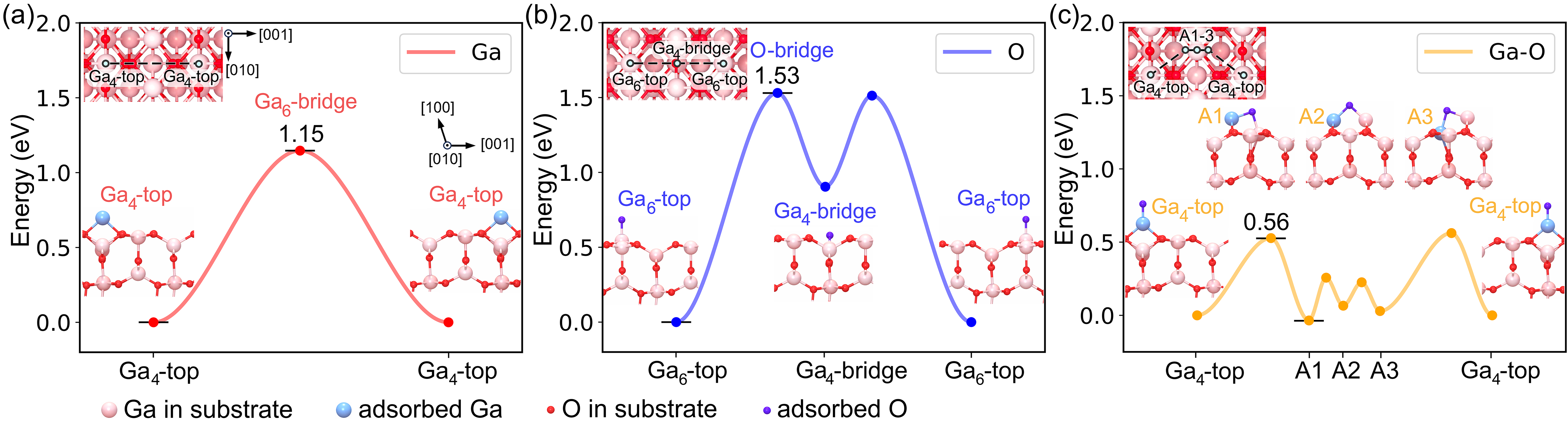
Before investigating atomic migrations at the miscut step edges, we first examine the migration behavior of Ga/O adatoms and Ga-O adatom pair on the flat \hkl(100) surface of -\ceGa2O3, as predicted by the ML model, as illustrated in Figure 1. We conducted a comprehensive search of atomic migration paths (detailed in Supporting Information Note 1, Figures S1 and S2, and Table S1), closely examining all the possible direct hopping/exchange migration paths. The MEPs in the \hkl[001]/\hkl[00-1] directions on the \hkl(100) surface involve direct hopping for the Ga/O adatoms (Figure 1a and 1b) and Ga exchange for the Ga-O adatom pair (Figure 1c). The corresponding MEBs for Ga adatom, O adatom, and Ga-O adatom pair were found to be 1.15 eV, 1.53 eV, and 0.56 eV, respectively. We also validated these ML-predicted MEPs and MEBs through DFT calculations (Supporting Information Note 1, Figure S4), which exhibited the same trends with reasonable deviation. Based on the ML and DFT results, the mobility of Ga adatom is consistently higher than that of O adatom. The Ga-O adatom pair can enhance the migration of surface adatoms, by facilitating the exchange migration path. These results provide important references for the subsequent exploration of atomic migration on the \hkl(100) surface with different miscut step edges.
We further investigated the MEPs and MEBs of Ga/O adatom migration on the -\ceGa2O3 \hkl(100) surface with two miscut step edges, as shown in Figure 2. The left step is a \hkl[00-1] step with a \hkl(-201) step-edge facet, and the right step is a \hkl[001] step with a \hkl(001) step-edge facet. The atomic migration paths at the step edges on the both sides were searched systematically (see Supporting Information, Note 2, Figure S5, and Tables S2 and S3). The MEPs on the terrace are the same as those on the flat \hkl(100) surface (Figure 1), whereas the MEBs exhibit marginal increases (1.29 eV vs. 1.15 eV for Ga and 1.65 eV vs. 1.53 eV for O), owing to the compressive strain effect of the stepped terrace.
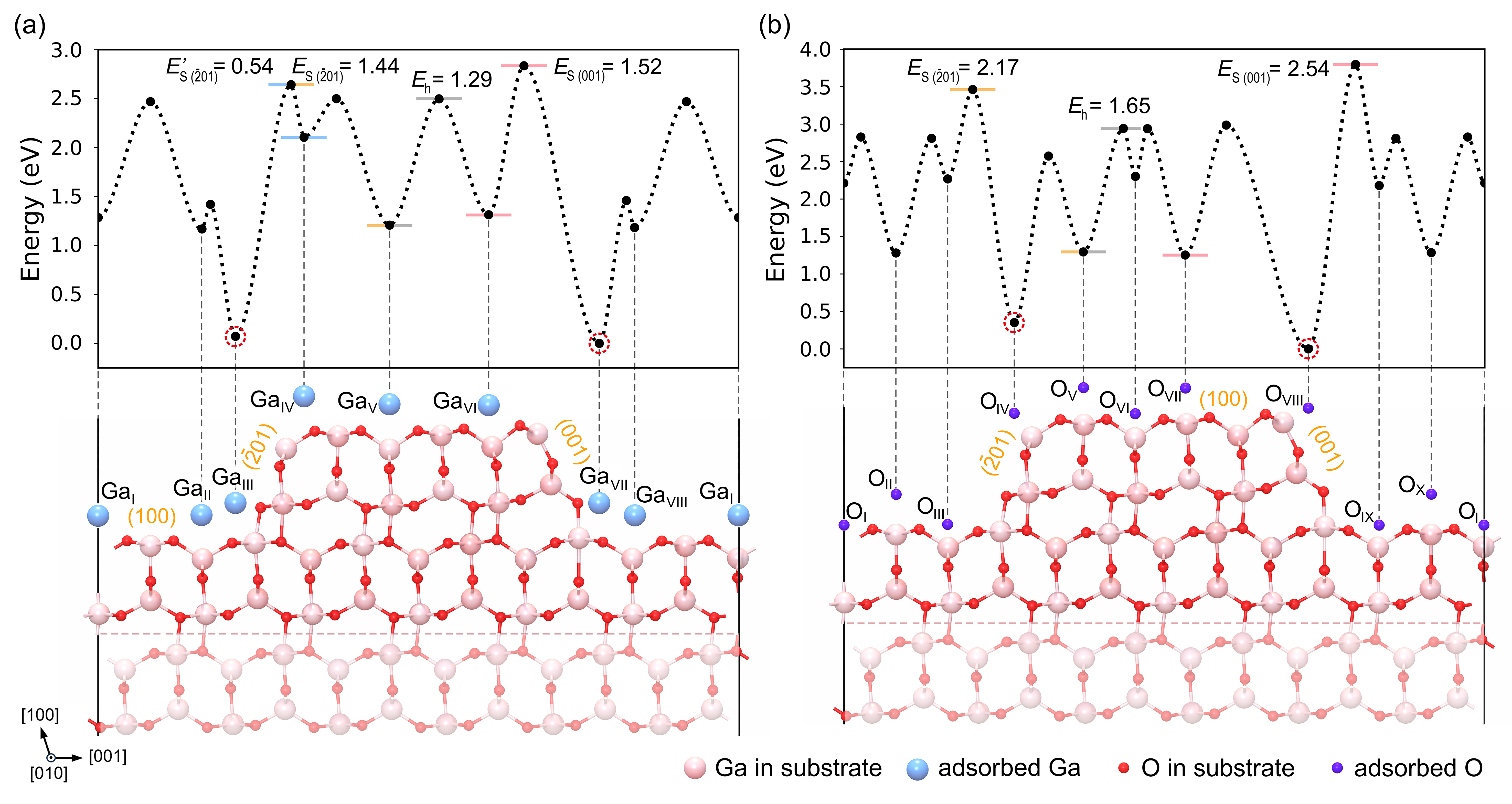
Importantly, the most striking observation is the distinct single- and two-stage ES barriers of Ga adatom, rooted from the asymmetric monoclinic lattice of -\ceGa2O3. As shown in Figure 2a, the overall MEB for migrating downward the \hkl[00-1] step edge () is eV. In comparison to the MEB climbing downward the \hkl[001] step edge (, eV), the energy difference in the ES barriers is not significant (0.15 eV vs. 0.23 eV). However, a two-stage MEP is revealed for migrating downward the \hkl[00-1] step edge, where the site serves as a metastable shallow valley with an effective downhill barrier of eV. In addition to the overall smaller \hkl[00-1] ES barrier (0.15 eV), this intermediate site (similar to an intermediate state in catalysis) can significantly promote the downhill migration of Ga adatom at the \hkl[00-1] step edge, thereby suppressing the formation of double-steps and hillocks on the terrace in the \hkl[00-1] miscut direction.
Additionally, the energies of Ga adatoms at the step-edge-bottom sites ( and ) are much lower, compared to the energies at the step-edge-top sites ( and ). These energy differences lead to a strong downhill migration trend for Ga adatoms at the step edge. These results have been validated by DFT calculations, which can be found in Supporting Information, Note 2, Figures S5 and S7. For comparison, we also calculated the MEBs of Ga adatoms on a step with the \hkl(-201) terrace and \hkl(100) step-edge surface (see Supporting Information, Note 2, Figure S8), showing a much higher MEBs and ES barriers. On the other hand, the MEBs of O adatom migration on both terrace and step edges are higher than those of Ga adtom, as shown in Figure 2b. Notably, unlike the stable Ga sites, the most stable sites near the step edges for O adatoms are the step-edge-top sites, which is expected for anions, as the step-edge-bottom sites are screened by the O anions carrying the same type of charge.
However, although the NEB calculations for the migration of Ga and O adatoms provide clear evidence on the edge-dependent step-flow growth mechanism, arising from the asymmetry of -\ceGa2O3 lattice, the manybody (such as Ga-O adatom pair and more) migration is too complicated to be effectively described by MEPs and MEBs. Therefore, we further conducted ML-MD simulations to elucidate the dynamic migration process for Ga/O adatoms, and Ga-O adatom pairs on a large-sized -\ceGa2O3 \hkl(100) facet with a miscut \hkl[00-1] step edge.
As shown in Figure 3a, in the random adatom migration simulations, Ga/O adatoms and Ga-O adatom pairs were deposited 10 times at each of the 11 different deposition sites, marked by yellow arrows. The final positions of the adatoms (and pairs) were tracked and counted after annealing for 1500 ps at 1200 K (see Supporting Information, Note 3 for details). The Ga-O adatom pairs tend to migrate quickly to the more stable vicinal sites of the step edges (Sites 1 and 11), exhibiting the highest mobility among the three species tested. Ga adatoms show the second-highest migration mobility, as indicated by the higher count at Site 1, while the distribution of the final O adatom sites remains relatively uniform, with no significant atomic migration. These statistics are in good agreement with the MEBs shown in Figure 1. Notably, the relatively high mobility of Ga adatom and Ga-O adatom pair leads to an essential assumption for the subsequent deposition ML-MD simulations, which consider terrace widths of a few nanometers and time spans of a few nanoseconds: Within a reasonable MD simulation time, the adatoms can migrate to the step-edge region across the full width of the terrace. Consequently, the epitaxial step-flow growth is insensitive to the initial deposition sites of adatoms, as low-mobility O adatoms can be mobilized by forming Ga-O adatom pairs upon encountering Ga adatoms.
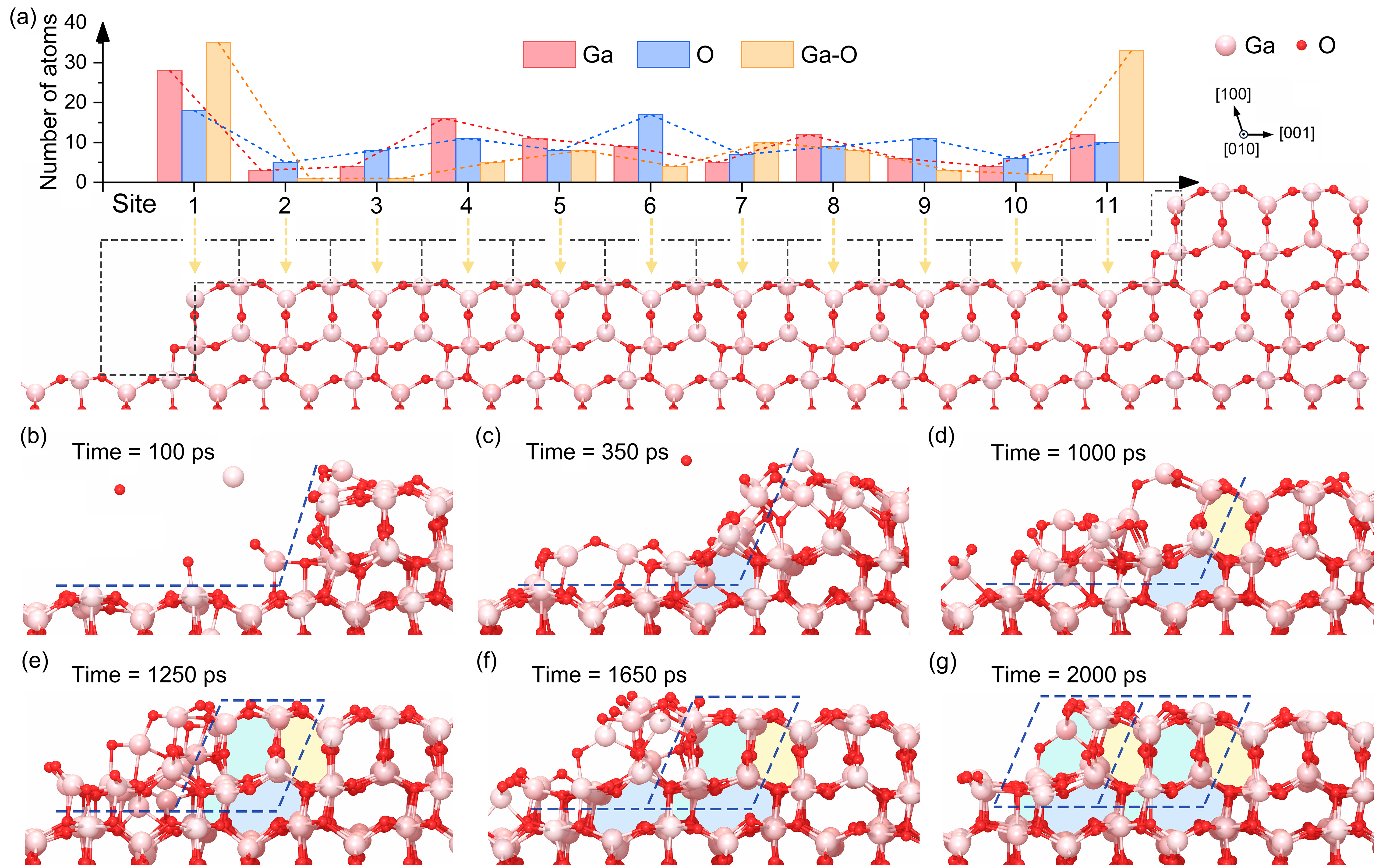
Based on this observation and discussion, we further simulated the dynamic processes of epitaxial growth at the -\ceGa2O3 \hkl(100)-\hkl[00-1] step edges, as shown in the snapshots in Figure 3b-g (More details in Supporting Information, Note 3, Figures S9 and S10, and Movies S1 and S2). The deposited adatoms near the step edge quickly bind to the edge-bottom site, and then grow epitaxially, completing the atomic rings in the sequence indicated by the “blue yellow cyan blue” shadows in Figure 3b-g. The epitaxial layer initially grows a half-layer extending the step edge (blue shadow in Figure 3c) before forming the upper half-layer near the step-edge surface (yellow and cyan shadows in Figure 3d and 3e). Once one period of the epitaxial \hkl(-201) step edge is completed, a second \hkl(-201) step-edge unit can be formed, repeating the step-flow growth process in the \hkl[00-1] direction (depicted by the additional blue, yellow, and cyan shadows in Figure 3f and 3g).
Meanwhile, the step-flow growth process at the \hkl(100)-\hkl[001] step edge can be investigated by ML-MD simulation, as shown in Supporting Information, Note 3, Figure S10. Notably, in contrast to the perfect step-flow growth observed at the \hkl[00-1] step edge, the nucleation of TBs was observed in the simulations at the \hkl[001] step edge. These findings are consistent with the previous experimental observations 32, 34, which reported significant lower quality of -\ceGa2O3 epitaxial films grown on the \hkl(100)-\hkl[001] step substrates compared to those grown on the \hkl(100)-\hkl[00-1] step substrates, primarily due to the high density of TBs. Our ML-MD simulations suggest that these TBs in the epitaxial films may originate from the deposited atoms near the \hkl[001] step edge or even from the structural transformations of the step edge itself.
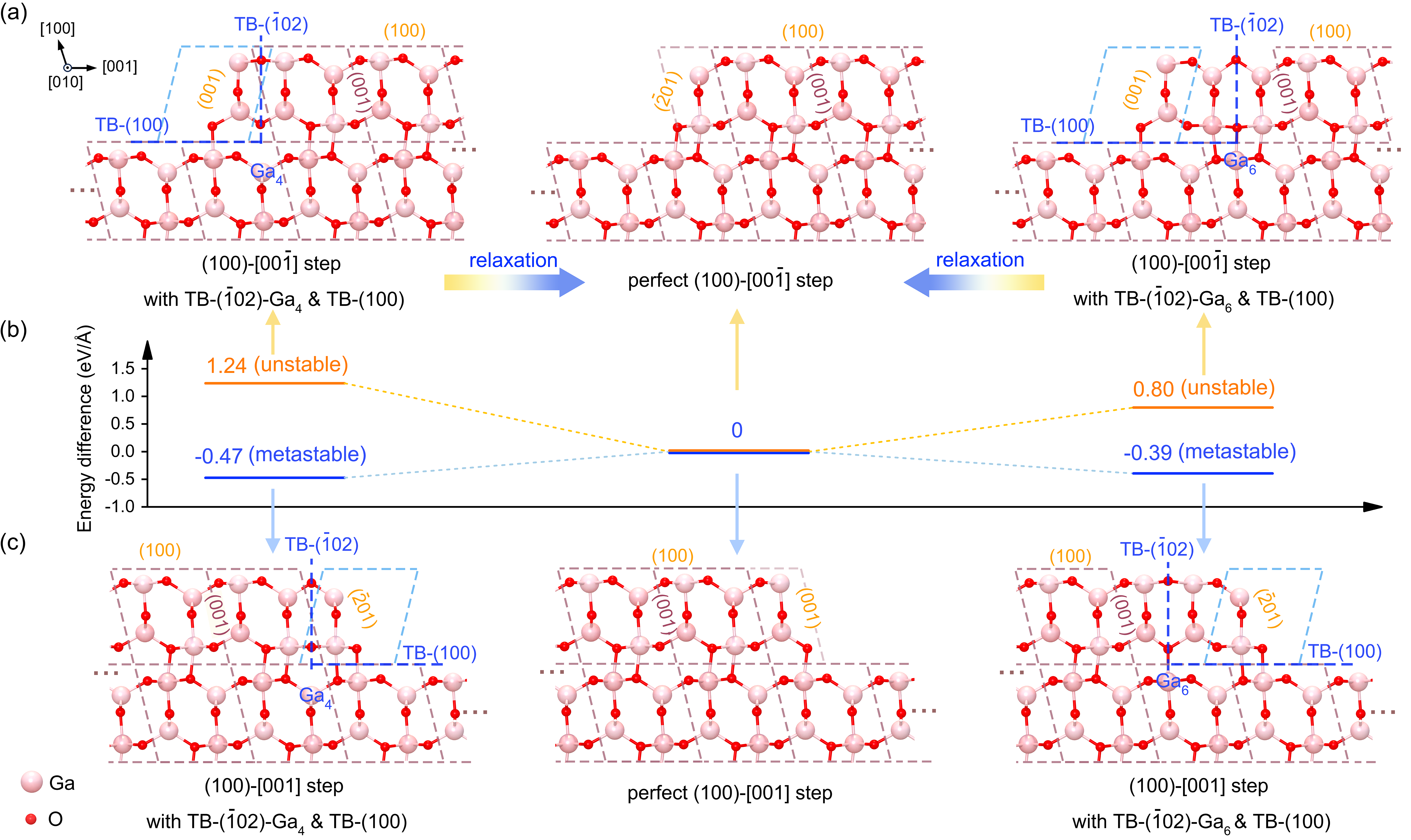
To explain why it is easier to form TBs on the \hkl[001] step compared to the \hkl[00-1] step, we conducted further static energy calculations for TB nucleation using the ML model. DFT calculations were also employed to ensure higher accuracy and provide cross-validation. As shown in Figure 4, we constructed the TBs on both the \hkl[00-1] and \hkl[001] step edges, considering two different types of atomic structures of TBs at each step edge. The two different TB structures for each step edge are distinguished by the different positions of TB-\hkl(-102) (Ga4 and Ga6 sites), as each twin at the step edge is composed of TB-\hkl(-102) and TB-\hkl(100). The relaxed structures of these steps with TBs are shown in Supporting Information, Note 4, Figure S11. The energy differences between the TB and perfect step configurations are shown in Figure 4b. For the \hkl[00-1] step, both TB structures shown in Figure 4a are energetically unstable and spontaneously relax back into the perfect step after structure relaxation. On the contrary, for the \hkl[001] step, both TB structures shown in Figure 4c are, rather surprisingly, energetically favorable, with energy differences of eV/Å and eV/Å compared to the perfect step. Therefore, while TBs are energetically unfavorable to form on the \hkl[00-1] step edge, they are energetically favorable and easy to form on the \hkl[001] step edge. Our results provide a direct explanation for the phenomena observed in previous experiments 32, 34 as well as in our ML-MD simulations.
Therefore, to achieve the high quality step-flow growth in the homoepitaxy of -\ceGa2O3, the selection of the orientation of substrates and the directions of miscuts are essential, which determines the terrace facet and step edge. It is important that atoms can migrate to the step-edge site efficiently, which requires that the migration energy of atoms on the terrace surface is low and the energy of atoms at the step-edge site is significantly lower than that of other sites, as shown in Figure 2 and Figure 3a. Furthermore, both the terrace and step edge surfaces should have good thermal stability to maintain the regular step surface. Notably, even when the above requirements are satisfied, an improper miscut direction can promote the formation of TBs. For instance, the \hkl(100)-\hkl[001] step edges illustrated in Figure 4 can facilitate TBs formation. In contrast, the atomic structures of the \hkl(100)-\hkl[00-1] step edges could effectively prevent the occurrence of TBs.
In this work, we investigated the atomic mechanisms of the step-flow growth on -\ceGa2O3 \hkl(100) facet using ML-MD and DFT methods. Ga adatom and Ga-O adatom pair are the primary atomic species responsible for efficient atomic migration on the \hkl(100) surface, both with and without a miscut, owing to their relatively low MEBs. The intrinsic lattice asymmetry of -\ceGa2O3 leads to a distinct two-stage ES barrier of Ga adatoms at the \hkl[00-1] step edge, favoring downhill migration towards the stable step-edge-bottom site. The periodic step-flow growth processes on the \hkl(100)-\hkl[00-1] and \hkl(100)-\hkl[001] step edges are revealed through ML-MD simulations at atomic resolution. Furthermore, the TB nucleation structures at the \hkl(100)-\hkl[001] step edge are proved to be energetically more favorable than the perfect step, while the TB structures on the \hkl(100)-\hkl[00-1] step edges are unstable. Our study clarifies the mechanisms of the step-flow growth on -\ceGa2O3 \hkl(100) substrates, providing an atom-level theoretical basis for the selection and processing of substrates to achieve high-quality -\ceGa2O3 epitaxial thin films.
1 Methodology
The ML-MD calculations in this word are performed using the Large-scale Atomic/Molecular Massively Parallel Simulator (LAMMPS) code 45. The ML interatomic potential was recently developed in our previous work 46 makes the large-scale MD simulations of \ceGa2O3 homoepitaxy feasible 29 and high-energy collision cascade. The atomic migration MEBs were calculated by the climbing-image nudged elastic band (CI-NEB) method with improved tangent estimation 47, 48, converging the forces to within eV/Å and energies to within eV. These NEB calculations were performed using 9 images between the initial and final structures. For MD simulations of the -\ceGa2O3 homoepitaxy and the migration of Ga/O atoms or Ga-O atomic pair on the step surface, the temperature were set as 1200 K. All the MD simulation cells consist of three groups of atoms depending on the initial positions: (i) the atoms in the fixed layer are fixed to avoid movement of the entire cell due to the momentum introduced by the incoming deposited atoms; (ii) the atoms in the thermal layer are controlled by Nosé-Hoover thermostat 49, 50; and (iii) the atoms in the surface layer, epilayer, and deposition zone are allowed to move freely following Newton’s law. More details on ML-MD calculations can be found in the Supporting Information, Note 3.
All of our DFT calculations are performed using Vienna Ab-initio Simulation Package (VASP) code 51 with the projected augmented-wave (PAW) method 52, employing 13 () and 6 () valence electrons for Ga and O atoms, respectively. The generalized gradient approximation (GGA) with Perdew-Burke-Ernzerhof (PBE) 53 functional is used for -correlation. The kinetic energy cutoff of the plane-wave is set to 520 eV. For structural optimization, the energy convergence criterion was eV, and the force convergence criterion was eV/Å. Gaussian approximated smearing with a width of 0.01 eV was used. The MEBs of atomic migration were calculated using the CI-NEB method by VASP-vtst 47, 48, converging the forces to within eV/Å. More details on DFT calculations can be found in the Supporting Information, Notes 1 and 4. The OVITO are used for the purpose of analyzing and visualizing the atomic configuration 54.
The energy differences () between the TB structures and perfect step are calculated by the following formula:
| (1) |
where the and are the energy of the TB structures and the energy of the perfect step structure, respectively; is the length of cells in the \hkl[010] direction, which is 6.17 Å in our work.
References
- Víllora et al. 2008 Víllora, E. G.; Shimamura, K.; Yoshikawa, Y.; Ujiie, T.; Aoki, K. Electrical conductivity and carrier concentration control in - by Si doping. Appl. Phys. Lett. 2008, 92, 202120, DOI: 10.1063/1.2919728
- Onuma et al. 2015 Onuma, T.; Saito, S.; Sasaki, K.; Masui, T.; Yamaguchi, T.; Honda, T.; Higashiwaki, M. Valence band ordering in - studied by polarized transmittance and reflectance spectroscopy. Jpn. J. Appl. Phys. 2015, 54, 112601, DOI: 10.7567/JJAP.54.112601
- Pearton et al. 2018 Pearton, S. J.; Yang, J.; Cary, P. H.; Ren, F.; Kim, J. H.; Tadjer, M. J.; Mastro, M. A. A review of materials, processing, and devices. Appl. Phys. Rev. 2018, 5, 011301, DOI: 10.1063/1.5006941
- Arora et al. 2018 Arora, K.; Goel, N.; Kumar, M.; Kumar, M. Ultrahigh performance of self-powered - Thin Film solar-blind photodetector grown on cost-effective Si substrate using high-temperature seed layer. ACS Photonics 2018, 5, 2391, DOI: 10.1021/acsphotonics.8b00174
- Kaur and Kumar 2021 Kaur, D.; Kumar, M. A strategic review on gallium oxide based deep-ultraviolet photodetectors: recent progress and future prospects. Adv. Opt. Mater. 2021, 9, 2002160, DOI: 10.1002/adom.202002160
- Sasaki et al. 2013 Sasaki, K.; Higashiwaki, M.; Kuramata, A.; Masui, T.; Yamakoshi, S. MBE grown and its power device applications. J. Cryst. Growth 2013, 378, 591–595, DOI: 10.1016/j.jcrysgro.2013.02.015
- Zhang et al. 2022 Zhang, J.; Dong, P.; Dang, K.; Zhang, Y.; Yan, Q.; Xiang, H.; Su, J.; Liu, Z.; Si, M.; Gao, J.; Kong, M.; Zhou, H.; Hao, Y. Ultra-wide bandgap semiconductor power diodes. Nat. Commun. 2022, 13, 3900, DOI: 10.1038/s41467-022-31664-y
- Higashiwaki and Jessen 2018 Higashiwaki, M.; Jessen, G. H. Guest Editorial: The dawn of gallium oxide microelectronics. Appl. Phys. Lett. 2018, 112, 060401, DOI: 10.1063/1.5017845
- Wang et al. 2021 Wang, Y.; Li, H.; Cao, J.; Shen, J.; Zhang, Q.; Yang, Y.; Dong, Z.; Zhou, T.; Zhang, Y.; Tang, W.; Wu, Z. Ultrahigh gain solar blind avalanche photodetector using an amorphous -based heterojunction. ACS Nano 2021, 15, 16654, DOI: 10.1021/acsnano.1c06567
- Aljarb et al. 2020 Aljarb, A. et al. Ledge-directed epitaxy of continuously self-aligned single-crystalline nanoribbons of transition metal dichalcogenides. Nat. Mater. 2020, 19, 1300–1306, DOI: 10.1038/s41563-020-0795-4
- Zhao et al. 2021 Zhao, J.; Huang, X.; Yin, Y.; Liao, Y.; Mo, H.; Qian, Q.; Guo, Y.; Chen, X.; Zhang, Z.; Hua, M. Two-dimensional gallium oxide monolayer for gas-sensing application. J. Phys. Chem. Lett. 2021, 12, 5813–5820, DOI: 10.1021/acs.jpclett.1c01393
- Yi et al. 2024 Yi, K. et al. Integration of high- native oxides of gallium for two-dimensional transistors. Nat. Electron. 2024, 7, 1126–1136, DOI: 10.1038/s41928-024-01286-x
- Vaidya et al. 2019 Vaidya, A.; Sarker, J.; Zhang, Y.; Lubecki, L.; Wallace, J.; Poplawsky, J. D.; Sasaki, K.; Kuramata, A.; Goyal, A.; Gardella, J. A.; Mazumder, B.; Singisetti, U. Structural, band and electrical characterization of - films grown by molecular beam epitaxy on Sn doped - substrate. J. Appl. Phys. 2019, 126, 095702, DOI: 10.1063/1.5113509
- Bin Anooz et al. 2020 Bin Anooz, S.; Grüneberg, R.; Wouters, C.; Schewski, R.; Albrecht, M.; Fiedler, A.; Irmscher, K.; Galazka, Z.; Miller, W.; Wagner, G.; Schwarzkopf, J.; Popp, A. Step flow growth of - thin films on vicinal (100) - substrates grown by MOVPE. Appl. Phys. Lett. 2020, 116, 182106, DOI: 10.1063/5.0005403
- Mauze et al. 2020 Mauze, A.; Zhang, Y.; Itoh, T.; Wu, F.; Speck, J. S. Metal oxide catalyzed epitaxy (MOCATAXY) of - films in various orientations grown by plasma-assisted molecular beam epitaxy. APL Mater. 2020, 8, 021104, DOI: 10.1063/1.5135930
- Chou et al. 2023 Chou, T.-S.; Rehm, J.; Bin Anooz, S.; Ernst, O.; Akhtar, A.; Galazka, Z.; Miller, W.; Albrecht, M.; Seyidov, P.; Fiedler, A.; Popp, A. Exploring miscut angle influence on (100) - homoepitaxial films growth: Comparing MOVPE growth with MBE approaches. J. Appl. Phys. 2023, 134, 195301, DOI: 10.1063/5.0170463
- Zhang et al. 2022 Zhang, T.; Cheng, Q.; Li, Y.; Hu, Z.; Ma, J.; Yao, Y.; Zhang, Y.; Zuo, Y.; Feng, Q.; Zhang, Y.; Zhou, H.; Ning, J.; Zhang, C.; Zhang, J.; Hao, Y. Investigation of the surface optimization of - films assisted deposition by pulsed MOCVD. Scr. Mater. 2022, 213, 114623, DOI: 10.1016/j.scriptamat.2022.114623
- Meng et al. 2024 Meng, L.; Yu, D.; Huang, H.-L.; Chae, C.; Hwang, J.; Zhao, H. MOCVD Growth of - on (001) Substrates. Cryst. Growth. Des. 2024, 24, 3737, DOI: 10.1021/acs.cgd.4c00060
- Kuang et al. 2024 Kuang, S.; Yang, Z.; Zhang, Z.; Sheng, Z.; Wei, S.; Chen, Y.; Xu, W.; Yang, Y.; Chen, D.; Qi, H.; Zhang, K. H. Transport and electronic structure properties of MBE grown Sn doped homo-epitaxial films. Mater. Today Phys. 2024, 48, 101555, DOI: 10.1016/j.mtphys.2024.101555
- Leach et al. 2018 Leach, J. H.; Udwary, K.; Rumsey, J.; Dodson, G.; Splawn, H.; Evans, K. R. Halide vapor phase epitaxial growth of - and - films. APL Mater. 2018, 7, 022504, DOI: 10.1063/1.5055680
- Sdoeung et al. 2021 Sdoeung, S.; Sasaki, K.; Masuya, S.; Kawasaki, K.; Hirabayashi, J.; Kuramata, A.; Kasu, M. Stacking faults: Origin of leakage current in halide vapor phase epitaxial (001) - Schottky barrier diodes. Appl. Phys. Lett. 2021, 118, 172106, DOI: 10.1063/5.0049761
- Isomura et al. 2020 Isomura, N.; Nagaoka, T.; Watanabe, Y.; Kutsuki, K.; Nishinaka, H.; Yoshimoto, M. Determination of Zn-containing sites in - film grown through mist chemical vapor deposition via X-ray absorption spectroscopy. Jpn. J. Appl. Phys. 2020, 59, 070909, DOI: 10.35848/1347-4065/ab9fdf
- Nishinaka et al. 2021 Nishinaka, H.; Nagaoka, T.; Kajita, Y.; Yoshimoto, M. Rapid homoepitaxial growth of (010) - thin films via mist chemical vapor deposition. Mater. Sci. Semicond. Process. 2021, 128, 105732, DOI: 10.1016/j.mssp.2021.105732
- Feng et al. 2019 Feng, Z.; Anhar Uddin Bhuiyan, A. F. M.; Karim, M. R.; Zhao, H. MOCVD homoepitaxy of Si-doped (010) - thin films with superior transport properties. Appl. Phys. Lett. 2019, 114, 250601, DOI: 10.1063/1.5109678
- Mazzolini et al. 2020 Mazzolini, P.; Falkenstein, A.; Wouters, C.; Schewski, R.; Markurt, T.; Galazka, Z.; Martin, M.; Albrecht, M.; Bierwagen, O. Substrate-orientation dependence of - (100), (010), (001), and (-201) homoepitaxy by indium-mediated metal-exchange catalyzed molecular beam epitaxy (MEXCAT-MBE). APL Mater. 2020, 8, 011107, DOI: 10.1063/1.5135772
- Ngo et al. 2020 Ngo, T. S.; Le, D. D.; Lee, J.; Hong, S.-K.; Ha, J.-S.; Lee, W.-S.; Moon, Y.-B. Investigation of defect structure in homoepitaxial (-201) - layers prepared by plasma-assisted molecular beam epitaxy. J. Alloys Compd. 2020, 834, 155027, DOI: 10.1016/j.jallcom.2020.155027
- Meng et al. 2022 Meng, L.; Bhuiyan, A. F. M. A. U.; Feng, Z.; Huang, H.-L.; Hwang, J.; Zhao, H. Metalorganic chemical vapor deposition of (100) - on on-axis substrates. J. Vac. Sci. Technol., A 2022, 40, 062706, DOI: 10.1116/6.0002179
- Goto et al. 2022 Goto, K.; Murakami, H.; Kuramata, A.; Yamakoshi, S.; Higashiwaki, M.; Kumagai, Y. Effect of substrate orientation on homoepitaxial growth of - by halide vapor phase epitaxy. Appl. Phys. Lett. 2022, 120, 102102, DOI: 10.1063/5.0087609
- Zhang et al. 2024 Zhang, J.; Zhao, J.; Chen, J.; Hua, M. Orientation-dependent atomic-scale mechanism and defect evolution in - thin film epitaxial growth. Appl. Phys. Lett. 2024, 124, 022102, DOI: 10.1063/5.0177093
- Mu et al. 2020 Mu, S.; Wang, M.; Peelaers, H.; Van de Walle, C. G. First-principles surface energies for monoclinic and and consequences for cracking of . APL Mater. 2020, 8, 091105, DOI: 10.1063/5.0019915
- Chou et al. 2021 Chou, T.-S.; Seyidov, P.; Bin Anooz, S.; Grüneberg, R.; Tran, T. T. V.; Irmscher, K.; Albrecht, M.; Galazka, Z.; Schwarzkopf, J.; Popp, A. Fast homoepitaxial growth of (100) - thin films via MOVPE. AIP Adv. 2021, 11, 115323, DOI: 10.1063/5.0069243
- Schewski et al. 2016 Schewski, R.; Baldini, M.; Irmscher, K.; Fiedler, A.; Markurt, T.; Neuschulz, B.; Remmele, T.; Schulz, T.; Wagner, G.; Galazka, Z.; Albrecht, M. Evolution of planar defects during homoepitaxial growth of - layers on (100) substrates-A quantitative model. J. Appl. Phys. 2016, 120, 225308, DOI: 10.1063/1.4971957
- Li et al. 2024 Li, Q.; Guan, X.; Zhong, Y.; Jia, Z.; Li, Y.; Lin, N. Structures, influences, and formation mechanism of planar defects on (100), (001) and (-201) planes in - crystals. Phys. Chem. Chem. Phys. 2024, 26, 12564–12572, DOI: 10.1039/D3CP04305C
- Schewski et al. 2018 Schewski, R. et al. Step-flow growth in homoepitaxy of - (100)-The influence of the miscut direction and faceting. APL Mater. 2018, 7, 022515, DOI: 10.1063/1.5054943
- Mazzolini et al. 2020 Mazzolini, P.; Falkenstein, A.; Galazka, Z.; Martin, M.; Bierwagen, O. Offcut-related step-flow and growth rate enhancement during (100) - homoepitaxy by metal-exchange catalyzed molecular beam epitaxy (MEXCAT-MBE). Appl. Phys. Lett. 2020, 117, 222105, DOI: 10.1063/5.0031300
- Chou et al. 2025 Chou, T.-S.; Rehm, J.; Bin Anooz, S.; Wouters, C.; Ernst, O.; Akhtar, A.; Galazka, Z.; Albrecht, M.; Fiedler, A.; Popp, A. Impurity-induced step pinning and recovery in MOVPE-grown (100) - film. Appl. Phys. Lett. 2025, 126, 022101, DOI: 10.1063/5.0242301
- Matsunami and Kimoto 1997 Matsunami, H.; Kimoto, T. Step-controlled epitaxial growth of SiC: High quality homoepitaxy. Mater. Sci. Eng. R Rep. 1997, 20, 125–166, DOI: 10.1016/S0927-796X(97)00005-3, R20
- Hong et al. 2005 Hong, W.; Lee, H. N.; Yoon, M.; Christen, H. M.; Lowndes, D. H.; Suo, Z.; Zhang, Z. Persistent step-glow growth of strained films on vicinal substrates. Phys. Rev. Lett. 2005, 95, 095501, DOI: 10.1103/PhysRevLett.95.095501
- Schwoebel and Shipsey 1966 Schwoebel, R. L.; Shipsey, E. J. Step Motion on Crystal Surfaces. J. Appl. Phys. 1966, 37, 3682–3686, DOI: 10.1063/1.1707904
- Ehrlich and Hudda 1966 Ehrlich, G.; Hudda, F. G. Atomic View of Surface Self‐Diffusion: Tungsten on Tungsten. J. Chem. Phys. 1966, 44, 1039–1049, DOI: 10.1063/1.1726787
- Schwoebel 1969 Schwoebel, R. L. Step Motion on Crystal Surfaces. II. J. Appl. Phys. 1969, 40, 614–618, DOI: 10.1063/1.1657442
- Pimpinelli et al. 1994 Pimpinelli, A.; Elkinani, I.; Karma, A.; Misbah, C.; Villain, J. Step motions on high-temperature vicinal surfaces. J. Phys.: Condens. Matter 1994, 6, 2661, DOI: 10.1088/0953-8984/6/14/005
- Paulin et al. 2001 Paulin, S.; Gillet, F.; Pierre-Louis, O.; Misbah, C. Unstable step meandering with elastic interactions. Phys. Rev. Lett. 2001, 86, 5538–5541, DOI: 10.1103/PhysRevLett.86.5538
- ZaŁuska–Kotur et al. 2012 ZaŁuska–Kotur, M. A.; Krzyżewski, F.; Krukowski, S. Emergence of regular meandered step structure in simulated growth of GaN(0001) surface. J. Cryst. Growth 2012, 343, 138–144, DOI: https://doi.org/10.1016/j.jcrysgro.2012.01.033
- Thompson et al. 2022 Thompson, A. P.; Aktulga, H. M.; Berger, R.; Bolintineanu, D. S.; Brown, W. M.; Crozier, P. S.; in ’t Veld, P. J.; Kohlmeyer, A.; Moore, S. G.; Nguyen, T. D.; Shan, R.; Stevens, M. J.; Tranchida, J.; Trott, C.; Plimpton, S. J. LAMMPS - a flexible simulation tool for particle-based materials modeling at the atomic, meso, and continuum scales. Comput. Phys. Commun. 2022, 271, 108171, DOI: 10.1016/j.cpc.2021.108171
- Zhao et al. 2023 Zhao, J.; Byggmästar, J.; He, H.; Nordlund, K.; Djurabekova, F.; Hua, M. Complex polymorphs explored by accurate and general-purpose machine-learning interatomic potentials. npj Comput. Mater. 2023, 9, 159, DOI: 10.1038/s41524-023-01117-1
- Henkelman et al. 2000 Henkelman, G.; Uberuaga, B. P.; Jónsson, H. A climbing image nudged elastic band method for finding saddle points and minimum energy paths. J. Chem. Phys. 2000, 113, 9901–9904, DOI: 10.1063/1.1329672
- Henkelman and Jónsson 2000 Henkelman, G. A.; Jónsson, H. Improved tangent estimate in the nudged elastic band method for finding minimum energy paths and saddle points. J. Chem. Phys. 2000, 113, 9978–9985, DOI: 10.1063/1.1323224
- Nosé 1984 Nosé, S. A molecular dynamics method for simulations in the canonical ensemble. Mol. Phys. 1984, 52, 255–268, DOI: 10.1080/00268978400101201
- Hoover 1985 Hoover, W. G. Canonical dynamics: Equilibrium phase-space distributions. Phys. Rev. A 1985, 31, 1695–1697, DOI: 10.1103/PhysRevA.31.1695
- Kresse and Furthmüller 1996 Kresse, G.; Furthmüller, J. Efficiency of ab-initio total energy calculations for metals and semiconductors using a plane-wave basis set. Comput. Mater. Sci. 1996, 6, 15–50, DOI: 10.1016/0927-0256(96)00008-0
- Blöchl 1994 Blöchl, P. E. Projector augmented-wave method. Phys. Rev. B 1994, 50, 17953–17979, DOI: 10.1103/PhysRevB.50.17953
- Perdew et al. 1996 Perdew, J. P.; Burke, K.; Ernzerhof, M. Generalized Gradient Approximation Made Simple. Phys. Rev. Lett. 1996, 77, 3865–3868, DOI: 10.1103/PhysRevLett.77.3865
- Stukowski 2009 Stukowski, A. Visualization and analysis of atomistic simulation data with OVITO–the Open Visualization Tool. Modelling Simul. Mater. Sci. Eng. 2009, 18, 015012, DOI: 10.1088/0965-0393/18/1/015012