Learnable Sparsification of Die-to-Die Communication via Spike-Based Encoding
Abstract.
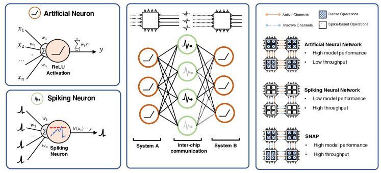
Efficient communication is central to both biological and artificial intelligence (AI) systems. In biological brains, the challenge of long-range communication across regions is addressed through sparse, spike-based signaling, minimizing energy consumption and latency. In contrast, modern AI workloads, which keep scaling ever larger across distributed compute systems, are increasingly constrained by bandwidth limitations, creating bottlenecks that hinder scalability and energy efficiency. Inspired by the brain’s efficient communication strategies, we propose SNAP, a hybrid neural network architecture that combines spiking neural networks (SNNs) and artificial neural networks (ANNs) to address these challenges. SNAP integrates SNNs at bandwidth-constrained regions, such as chip boundaries, where spike-based encoding reduces data transfer overhead. Within each chip, dense ANN computations are maintained to preserve high throughput, accuracy, and robustness.
Historically, SNNs have faced difficulties in scaling up, with limitations in task-specific performance and reliance on specialized hardware to exploit their sparsity. SNAP overcomes these barriers through an algorithm-architecture co-design that leverages learnable sparsity for die-to-die communication while limiting spiking layers to specific network partitions. This composable design integrates spike-based and non-spiking pathways, making it adaptable to diverse deep learning workloads. Our evaluations on language processing and computer vision tasks demonstrate up to 5.3 energy efficiency improvements and 15.2 reductions in inference latency, outperforming both traditional SNNs and non-spiking models. We find that as the model’s resources scale up, SNAP’s improvement margins grow. By addressing the critical bottleneck of inter-chip communication, SNAP offers a scalable and biologically inspired pathway to more efficient AI systems.
1. Introduction
The rapid expansion of artificial intelligence (AI) workloads has led to increasingly large and complex neural networks deployed across distributed computing systems. This scaling has intensified the challenges associated with data movement, particularly across chip boundaries, where bandwidth limitations and energy consumption become significant bottlenecks (Hennessy and Patterson, 2019). As models grow, exemplified by state-of-the-art architectures like OpenAI’s GPT-4 with over a trillion parameters (Patel and Wong, 2023), the inefficiency of dense, continuous data communication hinders scalability and performance.
Evolution has addressed the challenge of long-range communication in biological brains through sparse, spike-based signaling (Laughlin and Sejnowski, 2003). Neurons transmit information only when necessary, minimizing energy consumption and latency. This efficient, event-driven communication enables complex cognitive functions within a limited power budget.
Current approaches to mitigating data movement challenges in AI workloads involve both architectural and algorithmic strategies. Architectural solutions include advanced memory technologies like 3D stacked memory (Kurshan and Franzon, 2024) and high-bandwidth memory (HBM) (Lee et al., 2016), as well as improved interconnects and packaging techniques. However, they often face diminishing returns due to scaling constraints, such as thermal dissipation limits, fabrication complexity, and increased costs, making them less effective for addressing the exponential growth in data communication demands of large-scale AI systems.
Algorithmically, techniques such as model pruning, quantization, and structured sparsity reduce model size and computational load (Sze et al., 2017). Mixture-of-experts (MoE) models deactivate entire sub-networks to decrease data movement (Fedus et al., 2022). However, these methods can introduce trade-offs between efficiency and model accuracy or require complex training procedures.
Spiking Neural Networks (SNNs) offer a biologically inspired alternative, utilizing sparse, event-driven communication to process information (Roy et al., 2019). SNNs have demonstrated energy efficiency advantages due to their inherent sparsity and temporal dynamics. However, they have historically faced challenges in scaling up to match the performance of traditional Artificial Neural Networks (ANNs) on complex tasks. Difficulties in training, specialized hardware requirements, and degradation in task-specific performance have limited their widespread adoption (Pfeiffer and Pfeil, 2018).
To address the critical bottleneck of inter-chip communication while leveraging the strengths of both SNNs and ANNs, we propose SNAP (Scalable Neuromorphic Architecture for Polylithic Processing), a hybrid neural network architecture that integrates spiking neurons at chip boundaries. By employing spike-based encoding across bandwidth-constrained regions, such as die-to-die interfaces, we reduce data transfer overhead and energy consumption. Within each chip, dense ANN computations are maintained to ensure high throughput, accuracy, and robustness. A high-level overview is provided in Figure 1.
Our approach involves an algorithm-architecture co-design that strategically incorporates learnable sparsity for inter-chip communication. By limiting spiking layers to specific network partitions, we exploit the energy efficiency of SNNs without sacrificing the performance benefits of ANNs. This composable design integrates spike-based and non-spiking pathways, making it adaptable to a variety of deep learning workloads, including language processing and computer vision tasks.
We evaluate SNAP across multiple datasets and demonstrate significant improvements over traditional SNNs and non-spiking models. Our results show up to 5.3 enhancements in energy efficiency and 15.2 reductions in inference latency. These gains highlight the potential of biologically inspired communication strategies to overcome the limitations imposed by traditional hardware scaling laws.
In summary, the key contributions of this paper are:
-
•
Algorithmic Application of Hybrid Neural Networks (HNN): We propose a novel algorithm-architecture co-design that strategically maps SNN layers to bandwidth-constrained inter-die communication regions, while dense ANN layers handle high-throughput data processing within dies. This approach optimally partitions computation based on communication constraints and processing demands.
-
•
HNN Inter-Die Architecture: We design a hybrid inter-die architecture that integrates spiking and conventional artificial processing elements. It includes encoding conversion logic to bridge spiking and artificial layers, as well as a flexible interconnect fabric for routing mixed spike and dense data packets. This architecture supports efficient data flow management between spiking and non-spiking domains and ensures load balancing across partitioned neural networks.
-
•
Architectural Performance Gains: We evaluate fully spiking, fully artificial, and hybrid HNN models, demonstrating that as neural network size and processing element count scale, the proposed HNN approach achieves up to 15.2 speedup compared to conventional ANN implementations. Furthermore, we show comparable task accuracy across designs, with HNN delivering up to 5.3 energy efficiency improvements over ANN systems.
-
•
High-Level NoC Simulation Environment: We implement a Network-on-Chip (NoC) simulation framework capable of analyzing latency, throughput, and energy consumption for ANN, SNN, and HNN models. The framework calculates energy estimates for Extended-Mux I/O (EMIO), Memory (MEM), Processing Element (PE), and Router components and provides extensibility for custom layer definitions, enabling detailed performance modeling and architectural exploration.
The remainder of this paper is organized as follows: Section 2 provides background on the challenges of inter-chip communication and reviews related work. Section 3 details the SNAP architecture and its components. Section 4 describes our experimental setup and methodology. Section 5 presents and discusses our results. Finally, Sections 6 and 7 conclude the paper with related works and an outline of future directions.
2. Background
2.1. Spiking and Artificial Neural Networks
ANNs and SNNs can model similar network topologies but differ fundamentally in their neuron models. In ANNs, each artificial neuron computes a weighted sum of its inputs, followed by the application of a non-linear activation function. The output of an artificial neuron is expressed as:
| (1) |
where are weights, are inputs, is a bias term, and is the activation function.
In contrast, SNNs use spiking neurons, which can be viewed as binarized, linear recurrent neurons. Their output updates only when their hidden state, or ‘membrane potential’ exceeds a threshold . This behavior is often modeled using the leaky integrate-and-fire (LIF) neuron:
| (2) |
where is the decay factor, and is the weighted sum of input spikes with weights . The left hand side of the implication is the continuous-time equation governing the LIF neuron dynamics, and the right-hand side is one possible discrete-time equation that is implemented in-silico (Pedersen et al., 2024). For a step-by-step derivation, we refer the reader to Ref. (Eshraghian et al., 2023). A spike is emitted when:
| (3) |
where is the membrane potential, is the time constant of the LIF neuron model, is the resistance and denotes a current injection into the neuron. At each instance of time where exceeds a threshold , a spike is emitted as . Both spiking and artificial neurons are illustrated in Figure 1.
Information can be encoded with the spike signal in various ways, with rate encoding being the most common in SNN simulations (Adrian and Zotterman, 1926; Kim et al., 2022). In rate encoding, information is represented as the frequency of spikes over a given duration. While this introduces latency for static data, it enables sparse communication that reduces data movement and is well-suited for traversal through the NoC and chip-to-chip interconnects. Unlike deterministic multiplexing of activations across boundary layers, SNAP enables SNNs to learn optimized data representations and utilization of limited bandwidth, dynamically adapting to sparsity for improved efficiency.
In hybrid spiking and artificial neural networks, translating information between spiking and non-spiking representations is critical. For artificial layers to process spike-encoded data, the spike rate is accumulated over a defined time window to produce an equivalent activation value. Conversely, outputs from artificial neurons can be directly interpreted as target spike rates for spiking layers.
2.2. Hybrid Neural Networks
SNNs struggle to scale to larger sizes on their own. For example ‘SpikeGPT’ recently showed that the performance of a 1-B parameter architecture was not significantly greater than that of a 216-M parameter model. Hybrid models have been used to offset this performance gap of SNNs for some time, although they have not yet been adopted to partition workloads for the purposes of reducing data congestion. Rather, the ANN component is intended to enhance the performance loss from SNNs in most cases.
For instance, integrating non-spiking interneurons into SNNs has been shown to enhance biological fidelity and improve locomotion control in robotic systems (Liu et al., 2024). Hybrid models have been trained by interpolating between the single-bit regime of SNNs and the full-precision mode of ANNs (Voelker et al., 2020; Seekings et al., 2024). In many other works, ANNs are used as ‘read-out’ layers for SNNs to side-step non-differentiability when applying gradient descent (Fang et al., 2021).
Although not quite a hybrid network, the work in Ref. (Chang et al., 2023) combines an on-chip ANN and SNN for real-time target tracking, utilizing the SNN for high-speed targets and the ANN for robust performance. This is one of the few hardware implementations exploiting both network types concurrently. However, it does not address critical bottlenecks in neural network scaling, such as bandwidth and energy constraints. Extending this concept to optimize inter-chip communication could enable hybrid architectures to compete with state-of-the-art models by addressing scalability challenges while maintaining performance and efficiency.
3. SNAP: Scalable Neuromorphic Architecture for Polylithic Processing
In this section, we present SNAP, an inter-die architecture that combines spiking neurons for communication and artificial neurons for computation to address bandwidth bottlenecks in die-to-die communication. By partitioning neural networks across spiking and non-spiking domains and efficiently managing data flow across the die-to-die boundary, SNAP optimizes energy utilization and inference latency, enabling scalable and efficient large-scale systems. We evaluate SNAP across multiple datasets and models, comparing its performance to representative ANN and SNN baselines. Our approach demonstrates superior efficiency and scalability while remaining adaptable to alternative core designs. Detailed results, including metrics on energy consumption and latency, are presented in Section 5.
3.1. Proposed Algorithmic-Architecture Co-Design
To leverage the complementary benefits of SNN and ANN designs in a unified acceleration system, our architecture integrates a 2-D Mesh Network-on-Chip (NoC) with an grid of Core Tiles. Key components include an Extended Multiplexer IO (EMIO) block that interfaces with other chips/die and a Computational Cross-layer Packet (CLP) converter connected to each core controller, as depicted in Fig. 2. This CLP converter enables data conversion between spiking and artificial layers, ensuring efficient inter-layer communication across the system.
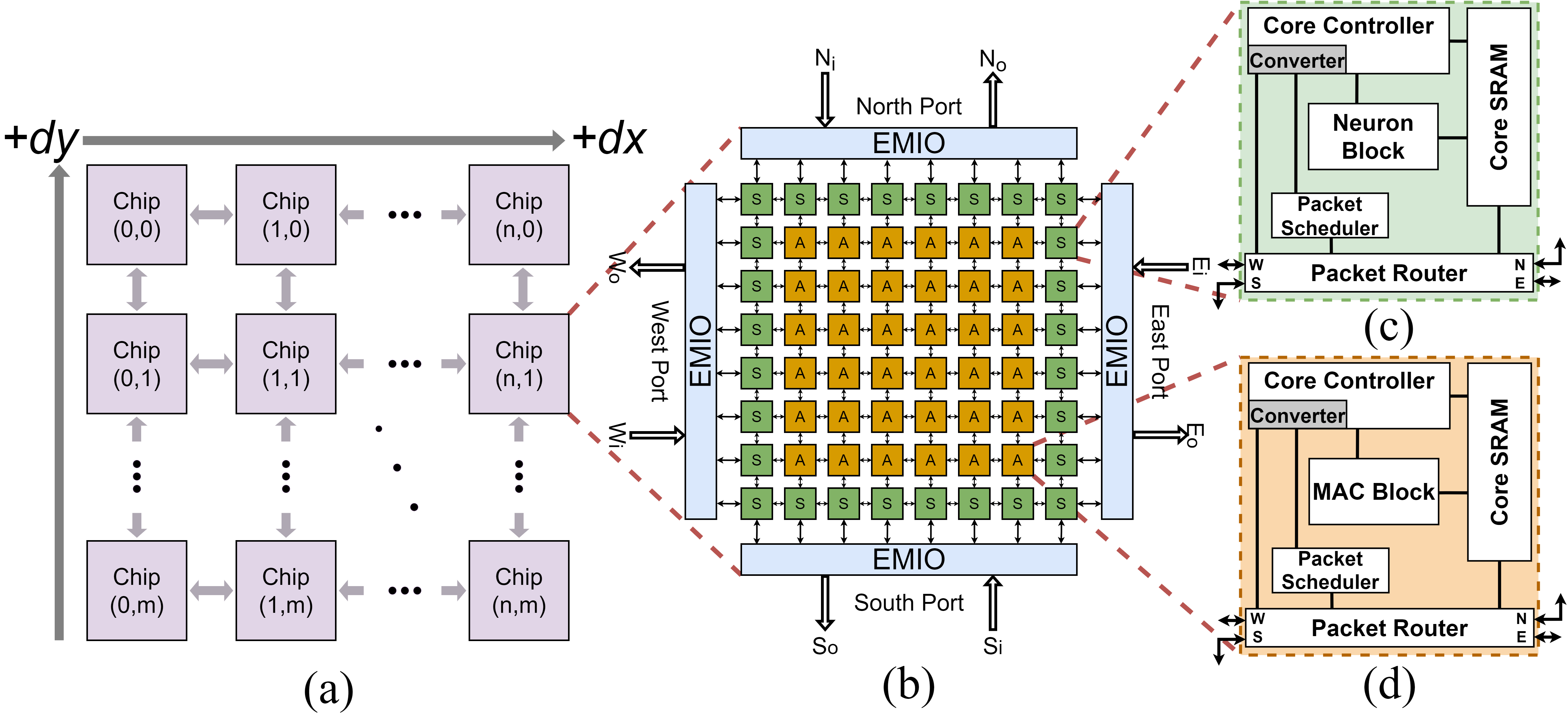
3.2. 2-D Mesh-based NoC Grid Design
We employ a NoC-based 2-D mesh design with static X-Y routing due to its scalability, reconfigurability, and simplicity. The NoC fabric consists of 28 spiking cores located at chip boundaries and 36 artificial cores centered within the chip. Both core types are designed to share common architecture blocks, with optimizations tailored to their respective neuron computations. Each core comprises five primary design blocks, as illustrated in Fig. 2.
Packet communication across cores is facilitated by deterministic X-Y routing handled by a Packet Router. The dx and dy fields within the packet header (Tab.5(a)) enable packets to traverse up to 256 cores before reaching a network-mapping repeater core for further routing. This configuration supports inter-chip communication across up to eight chips in any direction, with repeater cores extending communication as needed. To prevent deadlock, routing prioritizes the X (East/West) direction (Merolla et al., 2014a).
Table 1 provides detailed on-chip SRAM specifications for both ANN and SNN cores. The supply voltage for the architecture is set to the minimum supported by the 65nm process node library, ensuring efficient operation while maintaining compatibility with the technology node.
| Parameter | ANN | SNN | SNAP (HNN) |
|---|---|---|---|
| # Spiking Cores | - | 64 Cores | 28 Cores |
| # Artificial Cores | 64 Cores | - | 36 Cores |
| NoC frequency | 200 MHz | 200 MHz | 200 MHz |
| Supply voltage | 1.0V | 1.0V | 1.0V |
| On-Chip SRAM | 1.1 MB | 860 KB | 1 MB |
3.3. ANN & SNN Core Designs
| Parameters | Value |
|---|---|
| # neurons / # axons | 256 / 256 |
| # synapses | 64k |
| core SRAM | 13.75 KB |
| scheduler SRAM | 4 KB |
| MAC precision | 8b 8b |
| accumulator precision | 32b |
| weight precision | 32b |
| activation precision | 8b |
| Parameters | Value |
|---|---|
| # neurons / # axons | 256 / 256 |
| # synapses | 64k |
| core SRAM | 12.93 KB |
| scheduler SRAM | 0.5 KB |
| neuron potential precision | 8b |
| spike precision | 1b |
| weight precision | 8b |
SNAP incorporates both ANN and SNN cores, each designed as a synchronous, clock-driven module. While the core architectures are distinct in their components, they adhere to the core design principles established by platforms such as RANC and TrueNorth (Kim et al., 2018; Merolla et al., 2014a), with enhancements inspired by Eyerissv2 (Chen et al., 2019b). To maintain a homogeneous core array within SNAP, changes between ANN and SNN cores were minimized, focusing only on the differences essential for their respective computations. This streamlined, reconfigurable design allows for meaningful comparisons across ANN, SNN, and HNN accelerators, emphasizing performance and efficiency improvements in our benchmarks. Core parameters for ANN and SNN implementations are detailed in Tables 2(a) and 2(b), respectively.
Each core comprises a processing element (PE), a packet scheduler, and SRAM memory for storing weights and activations. A single core accommodates 256 neurons and axons, resulting in a system-wide total of over 64k synapses. This synapse count represents the maximum capacity of SNAP’s core grid, which places constraints on large-scale DNN implementations. Models with significantly higher synapse counts per layer, such as those with dense fully connected layers, must map connections across multiple hardware iterations. For instance, two fully connected layers of 256 neurons fully utilize the available synapse capacity. This highlights the importance of efficient resource allocation and connection mapping to enable the deployment of deeper and more complex networks within the hardware’s architectural limits.
The multiply-and-accumulate (MAC) units and accumulators within the PE of the ANN core are designed with 32-bit weights, 8-bit activations, an 8-bit8-bit MAC, and 32-bit accumulators. In contrast, the SNN core PE features 8-bit weights, 8-bit membrane potentials, and 1-bit spikes. These differences in bit width and precision influence the design of the scheduler and core SRAM, with values scaled accordingly to fit their respective requirements.
For the SNN core scheduler, the SRAM consists of 16256-bit entries to manage the 256 axons with a maximum delay of 16 ticks. This design enables temporal spike organization across all axons with a memory footprint of 0.5 KB per SNN core scheduler. In comparison, the ANN core scheduler SRAM is extended to accommodate the higher 8-bit activation precision, with 162048-bit entries totaling 4 KB per ANN core scheduler.
Similarly, the core SRAM is tailored to the requirements of each network. The SNN core features 256 410-bit entries, providing 12.93 KB of SRAM per core. These entries include synaptic connections, weights, potentials, neuron parameters (256 bits), packet destinations (124 bits), and delivery ticks (4 bits). For the ANN core, the SRAM is expanded to 256 440-bit entries, totaling 13.75 KB per core. This additional capacity accommodates the larger activation precision and associated parameters.
The Core Controller orchestrates the control path signals and is programmable to handle various layer types and computations. It interfaces with all core components, ensuring efficient data processing and coordination across the system. Specifically for SNN layer data communication, static dataset inputs must be encoded with multiple timesteps (as a buffered train of spikes) to encode information within the temporal domain. The 4-bit delivery time mentioned above has the ability to encode up to a 16-step spiking input. Utilizing higher time-steps in inputs increase the number of operations in the PE for a given spiking layer. Within dynamic datasets, we can utilize the temporal aspects of the inputs and do not need to encode the inputs across multiple timesteps.
3.4. EMIO Block Design
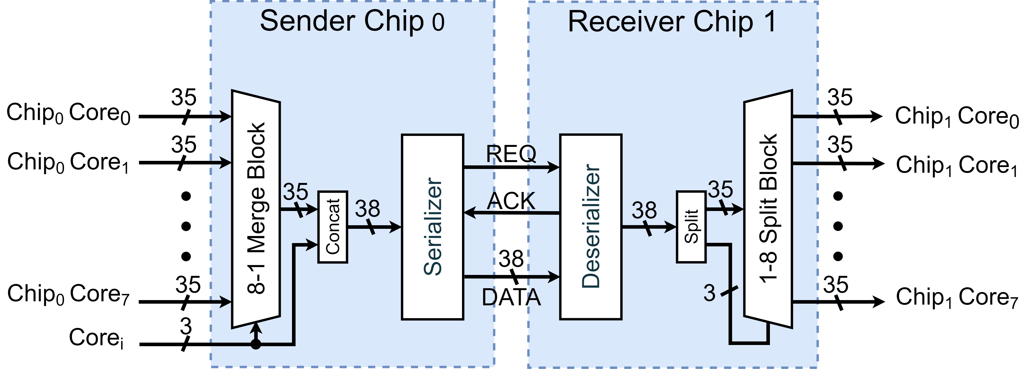
The Extended Mux I/O (EMIO) is a low-overhead interconnect designed to optimize die-to-die packet communication. This approach adapts elements from the TrueNorth interconnect design (Merolla et al., 2014a), scaling its merge-split block, originally interfacing 32 ports—to fit the 8 boundary spiking cores in our architecture. At the chip boundary, the NoC includes 64 unidirectional ports (32 input, 32 output) multiplexed down to 8 unidirectional ports at the I/O pads, enabling efficient communication while minimizing resource usage.
TrueNorth’s design exhibited a significant reduction in spike bandwidth—over 640 lower at the chip boundary compared to on-chip communication. This was caused by 2 serialization, 32-to-1 port multiplexing, and a 10 disparity between the NoC and I/O pad clock frequencies. Unlike TrueNorth’s asynchronous design, our EMIO employs a synchronous 200 MHz clock frequency at the chip boundary, eliminating clock disparities. As shown in Fig. 3, our design uses 8-to-1 port multiplexing with reduced serialization. A synthesized RTL implementation of our EMIO design revealed a die-to-die latency of 76 clock cycles for a single packet, with the serialization stage accounting for 38 cycles. Importantly, the serialization process occurs in parallel across the 8 peripheral ports connected to the boundary cores.
To support die-to-die communication, packets from the 8 peripheral cores are processed through a SerDes for transmission via the I/O pads. Each 35-bit packet is tagged with 3 additional bits for origin/destination mapping, resulting in a compact 38-bit format. The SerDes ensures efficient serialization, minimizing communication overhead and enabling precise packet routing across die-to-die interfaces. This design balances compactness and performance for high-throughput communication.
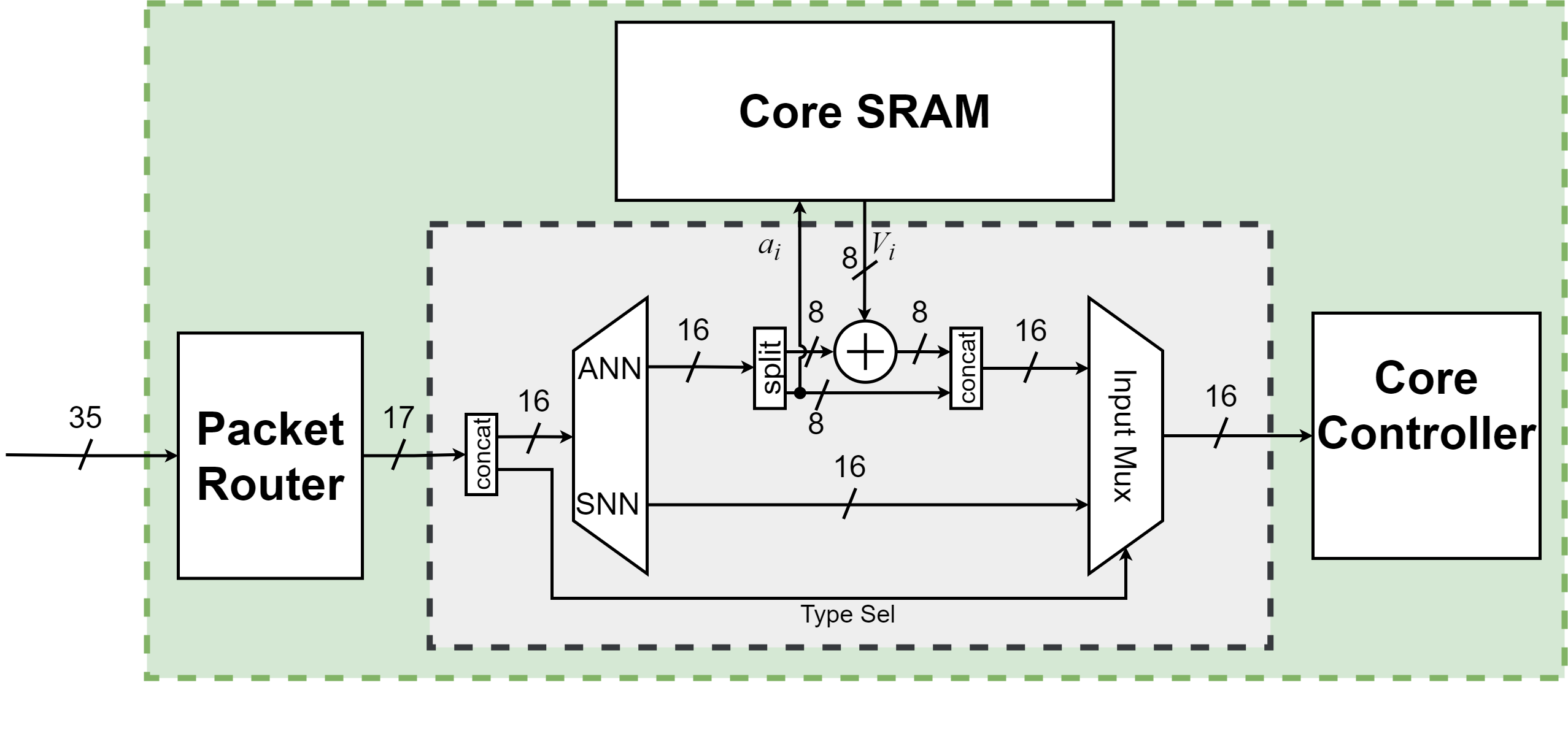
3.5. CLP Converter Design
| dx core destination | dy core destination | type | axon index |
| 9 bits | 9 bits | 1 bit | 8 bits |
| d-tick | padding |
| 4 bits | 4 bits |
| activation |
| 8 bits |
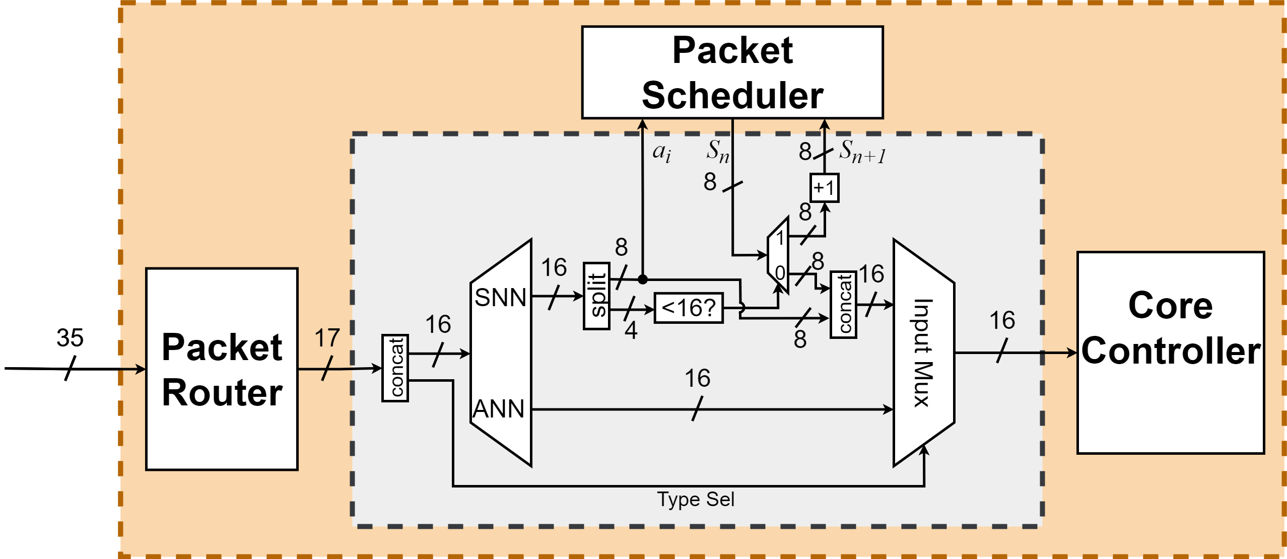
To enable conversion between spiking and artificial packets, the design incorporates a CLP converter for each of the 256 axons per core. This converter translates rate-encoded spiking packets into activation-encoded artificial packets and vice versa. The logical design, depicted in Fig.4, leverages the packet type field from Fig.5(a) to identify the packet format and perform parallel payload computation with minimal overhead.
For activation-to-spike conversion (Fig.4(a)), the CLP converter accesses the neuron’s membrane potential and directly adds the activation value. This process generates a rate-encoded spike sequence proportional to the activation value. For spike-to-activation conversion (Fig.4(b)), the CLP converter accumulates spikes over a specified maximum tick count, t, storing intermediate values in the Packet Scheduler. Once accumulated, the spike count for axon a is used to update the corresponding activation value, enabling efficient parallel updates before the data is forwarded to the Core Controller.
4. Methodology
4.1. Benchmark Models
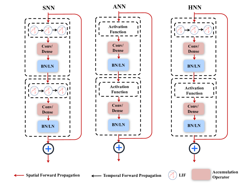
We integrate MS-ResNet (Hu et al., 2021), EfficientNet-B4 (Tan and Le, 2019), and RWKV (Peng et al., 2023) as representative architectures for computer vision and language models, respectively, to evaluate SNAP’s performance across diverse and challenging datasets. MS-ResNet18, a spike-driven variant of ResNet, is widely used in contemporary SNN research (Su et al., 2023; Yao et al., 2023; Lee et al., 2022) and is inherently compatible with both SNN and ANN architectures. The specific configuration of MS-ResNet18 is illustrated in Fig. 6. Unlike standard ResNet models, MS-ResNet18 employs membrane potential summation, enabling efficient spike-driven operations by modulating membrane potentials. For HNN-compatibility, each block uses LIF neurons, while inter-block connections maintain ANN compatibility, ensuring optimized input-output performance.
For language modeling, we leverage RWKV, a recurrent neural network (RNN)-based model designed as a lightweight alternative to transformers for language generation. RNN-based models like RWKV are particularly well-suited for integration with SNNs due to their inherent temporal processing capabilities. RWKV achieves competitive results compared to transformer-based architectures, with significantly lower computational overhead. In our implementation, we incorporate a residual connection similar to that used in MS-ResNet.
4.2. Simulation Environments
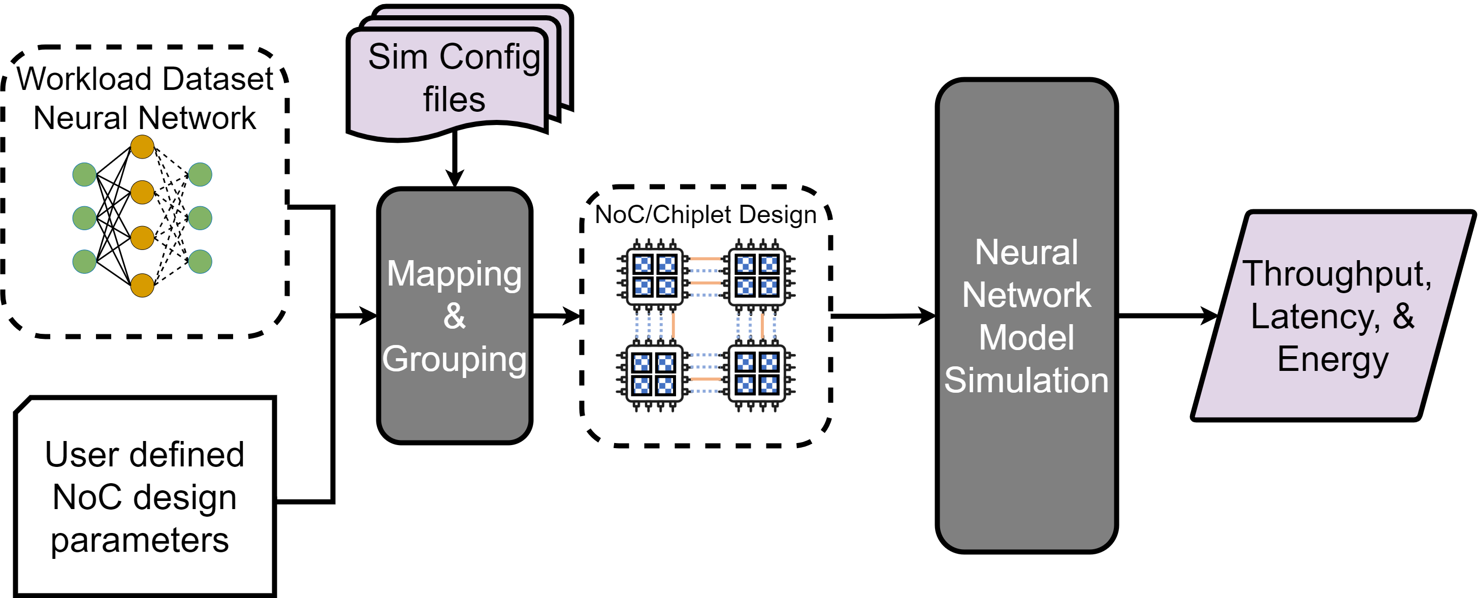
We developed a custom simulation environment for multi-chip accelerator systems to evaluate artificial, spiking, and hybrid networks with a focus on die-to-die communication. While existing simulators such as RANC and NN-Noxim (Kim et al., 2018; Kun-Chih and ting Yi, 2018) provide valuable tools for network evaluation, they are not specifically designed for modeling multi-chip, partitioned hybrid networks. To address this gap, we created a high-level simulation framework tailored for large-scale hybrid DNN models, offering flexibility for adding custom DNN layer definitions for SNNs, ANNs, and HNNs.
The simulation workflow, illustrated in Fig. 7, employs a co-designed approach where user-defined network workloads and NoC parameters are mapped onto the hardware. This enables layer-accurate simulation of large hybrid DNNs on custom architectures. The simulator adheres to a synchronous, clock-driven design for all ANN, SNN, and HNN components, mirroring the architectural behavior of the proposed system.
Energy and power calculations are based on the ORION 2.0 methodology (Kahng et al., 2009), which models Intel’s 65nm 80-core chip (Hoskote et al., 2007). The parameters were scaled for our design’s 1.0 V core supply voltage and 200 MHz NoC frequency, ensuring realistic energy efficiency results. Key simulation metrics include operations per layer, routed packets, and local packets. Operations correspond to MAC operations in ANN layers and accumulate (ACC) operations in SNN layers. Routed packets represent inter-core communication, calculated based on the average number of hops per packet using directional-X neural network mapping and X-Y packet routing equations (4) and (5). Local packets represent intra-core communication sent through the local port to the processing element (PE) for computation, providing a comprehensive evaluation of computational and communication overheads.
| (4) |
Where M is the middle core coordinates of the current layer and M is the middle core coordinates of the previous layer. The absolute Manhattan distance between layer midpoints approximates the average hops taken by a routed packet.
| (5) |
Calculating total number of routed packets in (5) is the number of local packets received through the local port multiplied by the number of average hops calculated in (4).
The scalable NoC simulators enabled us to model large, deep networks, including fully connected layers with over 19 million parameters. The three models—RWKV, MS-ResNet18, and EfficientNet-B4—were simulated with approximate workloads to evaluate system performance. For SNN models, we assumed a high input sparsity of 90% (10% spiking activity) and rate-encoded dataset inputs with a temporal window of = 8 time steps. This level of sparsity aligns with methodologies used in SNN accelerators such as SpinalFlow (Narayanan et al., 2020; Lemaire et al., 2022).
Following established methodologies discussed in prior work (Chen et al., 2020; Lemaire et al., 2022), we calculated the computational workload for both SNN and ANN layers, including convolutional, depthwise-convolutional, and pooling operations. For ANN models, operations were measured in terms of MAC, while for SNNs, operations were quantified as ACC counts, capturing the distinct computational requirements of each network type.
4.3. Latency Calculations
We measure latency and throughput for single-input inference by calculating the total MAC or ACC operations per layer. To ensure consistency, we assume a 1-cycle latency for both operations. Each processing element (PE) computes in parallel, leveraging the parallelism inherent in neural network layers. Total on-chip latency per layer is derived using equations (6) for ANN layers and (7) for SNN layers, reflecting the computational workload distributed across PEs.
| (6) |
| (7) |
where represents the number of neurons per layer and denotes the grouping of 256 neurons per core.
To incorporate the overhead of EMIO die-to-die latency, we account for a single packet transaction across the SerDes, estimated at 38 clock cycles for both input and output ports, resulting in a total of 76 cycles. The deserialization at the input port is pipelined, allowing the serial data stream to be expanded into parallel outputs during 38 of these 76 cycles. This pipelined deserialization is reflected in the calculation of latency overhead in (8).
| (8) |
where denotes the packets transmitted across the chip boundary and represents the number of cores in the peripheral neural network layer.
The total latency is computed using (9), which sums the -layer cycles of the SNN or ANN network and the -layer EMIO cycles for layers crossing chip boundaries. This formulation accounts for both intra-chip computation and inter-chip communication overhead.
| (9) |
4.4. Energy Consumption Calculations
We implemented an intra-chip energy model based on NN-Noxim and ORION 2.0 methodologies (Kun-Chih and ting Yi, 2018; Kahng et al., 2009), calculating energy consumption from the Tx and Rx transactions of routed and local packets, as defined in 5. This modular framework estimates power usage for core components—including the PE, memory (MEM), and router—across ANN, SNN, and HNN NoC designs.
Energy costs were normalized relative to MAC operations on 45nm (8-bit precision) and 65nm (16-bit precision) CMOS technologies (Dampfhoffer et al., 2023). Within our 65nm power model, PE energy is reduced as SNN inference consumes approximately 0.06 the energy of a MAC operation, reflecting the efficiency of accumulations compared to multiplications. SRAM read/write costs are scaled accordingly, with ANN weights at 32-bit precision and SNN weights at 8-bit precision as defined in the SNAP architecture.
For die-to-die energy modeling, EMIO costs are calculated relative to intra-chip core-to-core routing. Based on findings from TrueNorth (Merolla et al., 2014b), die-to-die data movement consumes 224 the energy of a core-to-core packet per hop. We scale router link energy by this factor to estimate boundary packet costs in our models. As EMIO link energy is consistent for both ANN and SNN packets, interconnect energy depends solely on the packet volume, directly influencing latency and overall consumption.
5. Results
5.1. Accuracy
| ANN | SNN | HNN | |
|---|---|---|---|
| # Enwik8 (PPL) | 2.66 | 2.92 | 2.57 |
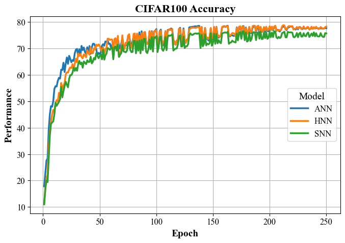
| CIFAR100 (Top-1 Acc) | 78.65% | 76.65% | 78.86% |
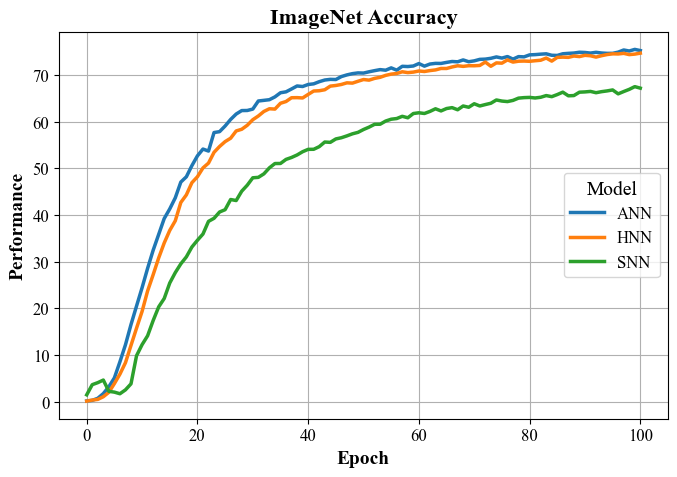
| ImageNet-1K (Top-1 Acc) | 75.48% | 67.50% | 74.78% |
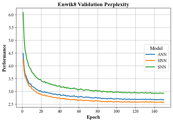
We employed MS-ResNet for image recognition and a six-layer, 512-size embedding RWKV model for language generation. For image recognition, experiments were conducted using the CIFAR100 (Krizhevsky and Hinton, 2009) dataset with MS-ResNet18 and the ImageNet-1K (Deng et al., 2009) dataset with EfficientNet-B4 (Tan and Le, 2019) modified to incorporate MS-ResNet blocks. For language generation, the Enwik8 (Mahoney, 2011) dataset was used. Results are summarized in Tab.3, with convergence curves illustrated in Fig.8.
Our findings show that HNNs outperform SNNs in both image classification and language generation tasks. Remarkably, HNNs also marginally outperform ANNs on CIFAR100 and Enwik8, while maintaining competitive performance on ImageNet-1K, outperforming SNNs by 7.28%. The superior performance of HNNs over SNNs is expected; however, the observed outperformance of HNNs over ANNs on CIFAR100 and Enwik8 is noteworthy. We hypothesize that SNN components in HNNs may act as a form of regularization, reducing overfitting on these datasets. For instance, on CIFAR100, ANNs demonstrated faster convergence compared to SNNs and HNNs, but HNNs ultimately achieved comparable or better performance. Similarly, on the larger ImageNet-1K dataset, which mitigates randomization effects due to its scale, HNNs maintained competitive results. These results highlight the potential of HNNs to surpass both SNNs and ANNs, particularly in tasks where overfitting is a concern, suggesting their viability for larger-scale applications.
5.2. Latency
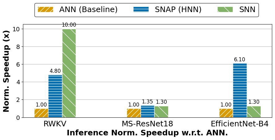
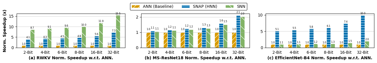
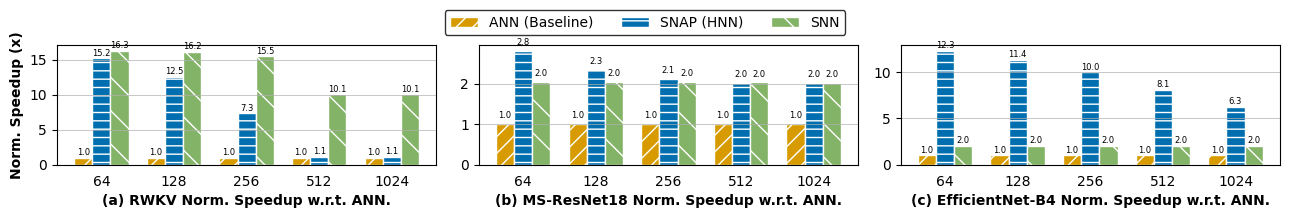
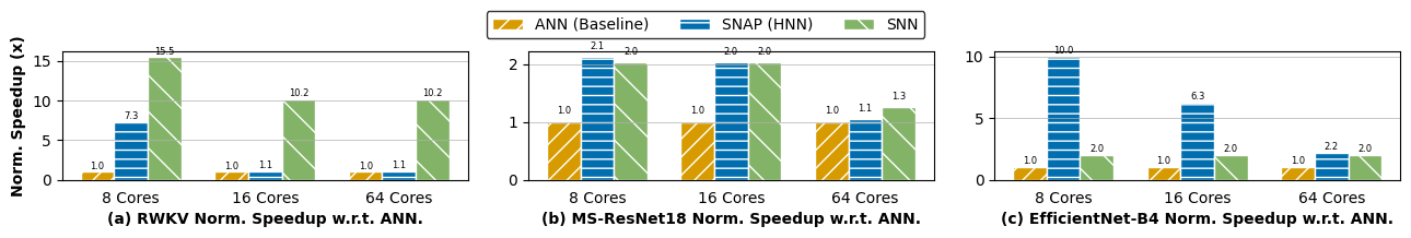
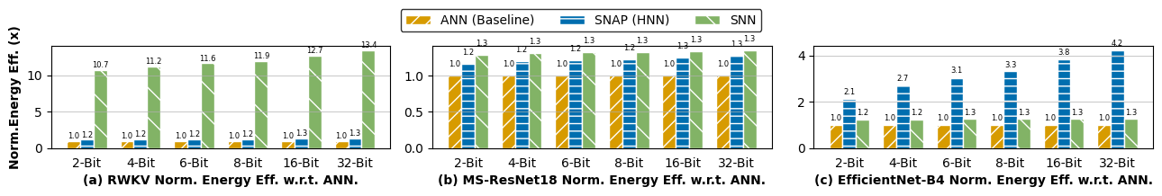
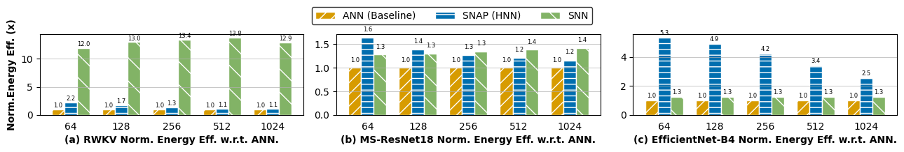
We mapped all software models to approximate workloads on the proposed ANN, SNN, and SNAP (HNN) designs, detailing the neuron, core, and chip resources utilized by each model. Using 8-bit precision, 256-neuron grouping, and an 8-core NoC configuration as a baseline, Fig. 9 presents our latency and accuracy reference metrics.
Across varying bit precisions, neuron groupings, and NoC dimensions, results demonstrate that HNNs achieve the fastest inference latency on static datasets, while SNNs maintain an advantage on dynamic datasets due to their reduced timesteps for achieving high accuracy. As shown in Figs. 11, 10, 12, SNAP exhibited speedups ranging from 1.1 to 15.2 over ANN models on benchmark datasets. Notably, as model resources scaled or bit-precision increased and die-to-die communication demands increased, HNNs demonstrated faster inference latency than both ANNs and SNNs, highlighting their scalability and efficiency in large-scale applications.
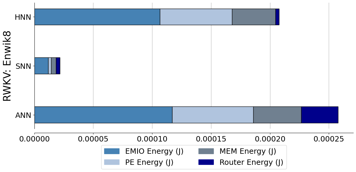
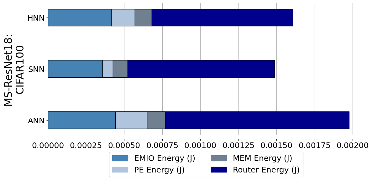
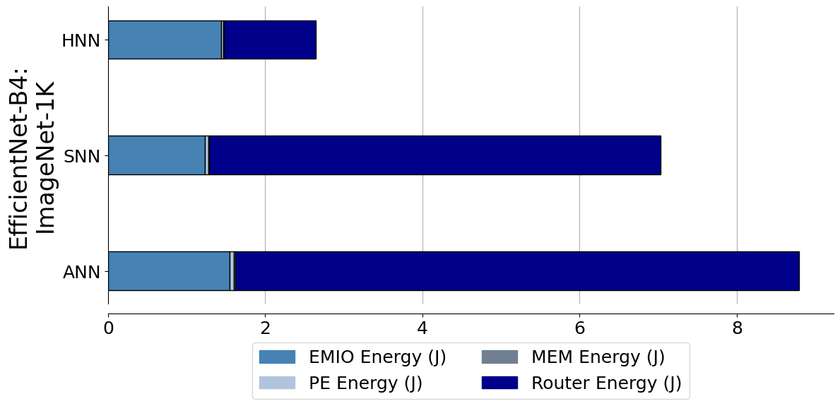
5.3. Energy
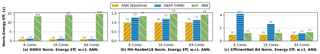
We found that the SNAP baseline model was 1 to 3.3 more energy efficient than the ANN design per inference. An energy breakdown per component is visible within Fig. 13. This efficiency arises from the computational cost reduction inherent in SNN layers, which allow HNNs to lower the total energy consumption per operation. As model sizes increase, the performance margin of SNAP further improves. While sweeping across other parameter configurations, energy efficiency gains continue up to 5.3 using a smaller neuron-to-processing-element grouping, which corresponds to allocating more resources per network.
For example, deploying EfficientNet-B4 on the ImageNet-1K dataset required 329 more chips than RWKV and approximately 73 times more chips than MS-ResNet-18, significantly increasing the number of die-to-die channels utilizing spike-based conversions. This scalability makes SNAP increasingly effective for large-scale models, avoiding the accuracy degradation commonly observed in purely SNN designs.
6. Related Work
Scalable Hardware Accelerators for SNN Workloads. Designs such as Loihi 2 from Intel (Davies et al., 2021), TrueNorth from IBM (Merolla et al., 2014a), ReckOn from ETH Zurich (Frenkel and Indiveri, 2022), and others (Frenkel et al., 2019; Narayanan et al., 2020; Painkras et al., 2013) offer highly scalable solutions for SNN workloads, achieving significant energy efficiency. SNN accelerators can outperform traditional Artificial Neural Networks (ANNs) in energy consumption by factors exceeding 1000× (Davies et al., 2021). However, SNN models and architectures have historically underperformed on standard benchmarks such as CIFAR-100 (Krizhevsky and Hinton, 2009) and ImageNet (Pfeiffer and Pfiel, 2018), with performance gaps widening on more complex tasks like language modeling (Zhu et al., 2023).
SNAP addresses these limitations through a hybrid design that integrates SNNs and ANNs. By leveraging the sparse nature of SNNs, inter-chip neuron signals can be transmitted efficiently, reducing the bandwidth and energy overhead associated with dense ANN communication. This reduces the stress on inter-chip throughput, which typically incurs high energy costs when transferring large amounts of data across long wires at high clock speeds. For instance, TrueNorth demonstrated the ability to send information at average neuron spiking rates as low as 12 Hz, consuming just 68 mW on complex recurrent networks (Merolla et al., 2014a). By adopting a hybrid approach, SNAP capitalizes on the strengths of SNN architectures while mitigating their limitations, offering an energy-efficient and scalable solution for large-scale tasks.
Scalable Hardware accelerators for ANN workloads ANN-based NoC accelerators (Chen et al., 2019b, a; Gao et al., 2017) have driven significant advancements in scalable and flexible chip-tiling designs. These architectures enable efficient die-to-die communication, low latency, high energy efficiency, and large-scale parallelism for DNN workloads. However, unlike SNAP, ANN-centric designs face inherent limitations in power consumption and performance when addressing sparsity in network workloads.
While many ANN accelerators focus on extreme reconfigurability of the NoC fabric (Lu et al., 2021), their optimization is often task-specific. SNAP addresses these challenges by offering a unified platform capable of custom DNN mapping across both SNN and ANN layers, achieving greater flexibility and efficiency in hybrid workloads. This makes SNAP a versatile solution for scaling large DNNs with reduced energy and latency overhead.
Scalable Hardware accelerators for HNN workloads NEBULA (Singh et al., 2020) is a neuromorphic, low-power chip that integrates both SNN and ANN neural cores, enabling flexible processing and leveraging “Hybrid Mode” for SNN-ANN hybrid networks. Similarly, (Dampfhoffer et al., 2023) explores Hybrid ANN-SNN architectures, where initial layers are processed using ANNs and subsequent layers with SNNs. These approaches demonstrate the potential of combining the strengths of both architectures for energy-efficient computation.
Despite these advancements, research on custom hardware-aware HNN designs, like SNAP, remains limited. SNAP distinguishes itself by optimizing the configuration of ANN and SNN cores, particularly through the placement of SNN layers at chip boundaries to reduce inter-chip communication overhead. To the best of our knowledge, neither NEBULA nor other related works explicitly address this strategic utilization of SNNs for minimizing inter-chip traffic, positioning SNAP as a unique and scalable solution for HNN workloads.
7. Conclusion
As deep learning workloads continue to scale, computational demands increasingly exceed the rate at which data can be transferred on-chip, creating significant bottlenecks. SNNs, with their sparse, spike-based activations, offer reduced communication traffic and improved energy efficiency compared to conventional ANNs.
In this paper, we introduced SNAP (Scalable Neuromorphic Architecture for Polylithic Processing), an HNN architecture that mitigates these bottlenecks by combining the strengths of SNNs and ANNs. By employing sparse SNN neurons at the periphery of the chip, near I/O bottlenecks, and dense ANN neurons within the chip interior, SNAP balances the trade-offs between accuracy and communication efficiency. This partitioned design allows the ANN layers to deliver high accuracy, while the SNN layers significantly alleviate bandwidth constraints across chip boundaries and within the NoC.
Our evaluations demonstrate that SNAP achieves up to 15.2 speedup over traditional ANN architectures on static data, using a smaller neuron-to-processing-element grouping, while maintaining similar accuracy and significantly improving energy efficiency. The improvements continue to scale relative to ANN-only accelerators, given the larger number of chip boundaries or higher bit-precision data that induce packet congestion. These results highlight the potential of hybrid architectures to address the scalability challenges of modern deep learning workloads, particularly in bandwidth-constrained environments.
Future work will focus on extending SNAP’s capabilities to larger-scale systems and exploring its applicability to emerging workloads, including transformers and graph neural networks, further establishing its role as a scalable and energy-efficient solution for advanced deep learning architectures.
References
- (1)
- Adrian and Zotterman (1926) Edgar D Adrian and Yngve Zotterman. 1926. The impulses produced by sensory nerve-endings: Part II. The response of a Single End-Organ. The Journal of physiology 61, 2 (1926), 151.
- Chang et al. (2023) Muya Chang, Ashwin Sanjay Lele, Samuel D Spetalnick, Brian Crafton, Shota Konno, Zishen Wan, Ashwin Bhat, Win-San Khwa, Yu-Der Chih, Meng-Fan Chang, et al. 2023. A 73.53 TOPS/W 14.74 TOPS heterogeneous RRAM in-memory and SRAM near-memory SoC for hybrid frame and event-based target tracking. In 2023 IEEE International Solid-State Circuits Conference (ISSCC). IEEE, 426–428.
- Chen et al. (2020) Kun-Chih Chen, Masoumeh Ebrahimi, Ting-Yi Wang, and Yuch-Chi Yang. 2020. A NoC-based simulator for design and evaluation of deep neural networks. Microprocessors and Microsystems 77 (2020) (2020).
- Chen et al. (2019a) Yu-Hsin Chen, Tushar Krishna, and Joel S. Emer. 2019a. NeuronLink: An Efficient Chip-to-Chip Interconnect for Neuromorphic Computing. In Proceedings of the International Symposium on Low Power Electronics and Design. 1–6. https://doi.org/10.1145/3341325.3342030
- Chen et al. (2019b) Yu-Hsin Chen, Tien-Ju Yang, Joel Emer, and Vivienne Sze. 2019b. Eyeriss v2: A flexible accelerator for emerging deep neural networks on mobile devices. IEEE Journal on Emerging and Selected Topics in Circuits and Systems 9, 2 (2019), 292–308.
- Dampfhoffer et al. (2023) Manon Dampfhoffer, Thomas Mesquida, Alexandre Valentian, and Lorena Anghel. 2023. Are SNNs Really More Energy-Efficient Than ANNs? an In-Depth Hardware-Aware Study. IEEE Transactions on Emerging Topics in Computational Intelligence 7, 3 (2023), 731–741. https://doi.org/10.1109/TETCI.2022.3214509
- Davies et al. (2021) Mike Davies, Alex Neckar, Kenneth Lai, Steve Goetz, Tobi Lin, Vikram Chandra, Matt Chou, Sylvain Cardin, and Steve Esser. 2021. Loihi2: A neuromorphic research chip combining spike-based learning and data-driven plasticity. arXiv preprint arXiv:2108.03229 (2021).
- Deng et al. (2009) Jia Deng, Wei Dong, Richard Socher, Li-Jia Li, Kai Li, and Li Fei-Fei. 2009. Imagenet: A large-scale hierarchical image database. In 2009 IEEE conference on computer vision and pattern recognition. Ieee, 248–255.
- Eshraghian et al. (2023) Jason K Eshraghian, Max Ward, Emre O Neftci, Xinxin Wang, Gregor Lenz, Girish Dwivedi, Mohammed Bennamoun, Doo Seok Jeong, and Wei D Lu. 2023. Training spiking neural networks using lessons from deep learning. Proc. IEEE (2023).
- Fang et al. (2021) Wei Fang, Zhaofei Yu, Yanqi Chen, Tiejun Huang, Timothée Masquelier, and Yonghong Tian. 2021. Deep residual learning in spiking neural networks. Advances in Neural Information Processing Systems 34 (2021), 21056–21069.
- Fedus et al. (2022) William Fedus, Barret Zoph, and Noam Shazeer. 2022. Switch transformers: Scaling to trillion parameter models with simple and efficient sparsity. Journal of Machine Learning Research 23, 120 (2022), 1–39.
- Frenkel and Indiveri (2022) Charlotte Frenkel and Giacomo Indiveri. 2022. ReckOn: A 28nm sub-mm2 task-agnostic spiking recurrent neural network processor enabling on-chip learning over second-long timescales. In 2022 IEEE International Solid-State Circuits Conference (ISSCC), Vol. 65. IEEE, 1–3.
- Frenkel et al. (2019) Charlotte Frenkel, Martin Lefebvre, Jean-Didier Legat, and David Bol. 2019. A 0.086-mm2 12.7-pJ/SOP 65k-Synapse 256-Neuron Online-Learning Digital Spiking Neuromorphic Processor in 28-nm CMOS. IEEE Transactions on Biomedical Circuits and Systems, Vol. 13, NO. 1, February 2019 (2019).
- Gao et al. (2017) Mingyu Gao, Jing Pu, Xuan Yang, Mark Horowitz, and Christos Kozyrakis. 2017. Tetris: Scalable and efficient neural network acceleration with 3d memory. In Proceedings of the Twenty-Second International Conference on Architectural Support for Programming Languages and Operating Systems. 751–764.
- Hennessy and Patterson (2019) John L Hennessy and David A Patterson. 2019. A new golden age for computer architecture. Commun. ACM 62, 2 (2019), 48–60.
- Hoskote et al. (2007) Yatin Hoskote, Sriram Vangal, Arvind Singh, Nitin Borkar, and Shekhar Borkar. 2007. A 5-Ghz Mesh Interconnect for a Teraflops PRocessor. IEEE Micro (2007).
- Hu et al. (2021) Yifan Hu, Lei Deng, Yujie Wu, Man Yao, and Guoqi Li. 2021. Advancing Spiking Neural Networks towards Deep Residual Learning. arXiv preprint arXiv:2112.08954 (2021).
- Kahng et al. (2009) Andrew Kahng, Bin Li, Li-Shiuan Peh, and Kambiz Samadi. 2009. ORION 2.0: A Fast and Accurate NoC Power and Area Model for Early-Stage Design Space Exploration. 2009 Design, Automation & Test in Europe Conference & Exhibition (2009).
- Kim et al. (2018) Jonghoon K. Kim, Joonhyung K. Kim, and Jongsun P. Kim. 2018. RANC: Reconfigurable Architecture for Neuromorphic Computing. In Proceedings of the International Conference on Reconfigurable Computing and FPGAs. 1–6. https://doi.org/10.1109/ReConFig.2018.8641707
- Kim et al. (2022) Youngeun Kim, Hyoungseob Park, Abhishek Moitra, Abhiroop Bhattacharjee, Yeshwanth Venkatesha, and Priyadarshini Panda. 2022. Rate coding or direct coding: Which one is better for accurate, robust, and energy-efficient spiking neural networks?. In ICASSP 2022-2022 IEEE International Conference on Acoustics, Speech and Signal Processing (ICASSP). IEEE, 71–75.
- Krizhevsky and Hinton (2009) Alex Krizhevsky and Geoffrey Hinton. 2009. Learning multiple layers of features from tiny images. Technical Report. University of Toronto, Toronto, ON, Canada.
- Kun-Chih and ting Yi (2018) Chen Kun-Chih and Wang ting Yi. 2018. NN-Noxim: High-Level Cycle-Accurate NoC-based Neural Networks Simulator. IEEE Access 8 (2018), 108527–108539. https://doi.org/10.1109/ACCESS.2018.3002082
- Kurshan and Franzon (2024) Eren Kurshan and Paul Franzon. 2024. Towards 3D AI Hardware: Fine-Grain Hardware Characterization of 3D Stacks for Heterogeneous System Integration & AI Systems. arXiv preprint arXiv:2409.10539 (2024).
- Laughlin and Sejnowski (2003) Simon B Laughlin and Terrence J Sejnowski. 2003. Communication in neuronal networks. Science 301, 5641 (2003), 1870–1874.
- Lee et al. (2022) Donghyun Lee, Guoqi Li, Hongsik Jeong, and Dong-Hyeok Lim. 2022. QAD-SNN: Quantization-aware Distillation on Spiking Neural Network. Korea Artificial Intelligence Conference (KAIC) (2022).
- Lee et al. (2016) Jong Chern Lee, Jihwan Kim, Kyung Whan Kim, Young Jun Ku, Dae Suk Kim, Chunseok Jeong, Tae Sik Yun, Hongjung Kim, Ho Sung Cho, Sangmuk Oh, et al. 2016. High bandwidth memory (HBM) with TSV technique. In 2016 International SoC Design Conference (ISOCC). IEEE, 181–182.
- Lemaire et al. (2022) Edgar Lemaire, Loïc Cordone, Andrea Castagnetti, Pierre-Emmanuel Novac, Jonathan Courtois, and Benoît Miramond. 2022. An analytical estimation of spiking neural networks energy efficiency. In International Conference on Neural Information Processing. Springer, 574–587.
- Liu et al. (2024) Faqiang Liu, Hao Zheng, Songchen Ma, Weihao Zhang, Xue Liu, Yansong Chua, Luping Shi, and Rong Zhao. 2024. Advancing brain-inspired computing with hybrid neural networks. National Science Review 11, 5 (2024), nwae066.
- Lu et al. (2021) Anni Lu, Xiaochen Peng, Yandong Luo, Shanshi Huang, and Shimeng Yu. 2021. A runtime reconfigurable design of compute-in-memory based hardware accelerator. In 2021 Design, Automation & Test in Europe Conference & Exhibition (DATE). IEEE, 932–937.
- Mahoney (2011) Matt Mahoney. 2011. Large text compression benchmark.
- Merolla et al. (2014b) Paul A Merolla, John V Arthur, Rodrigo Alvarez-Icaza, Andrew S Cassidy, Jun Sawada, Filipp Akopyan, Bryan L Jackson, Nabil Imam, Chen Guo, Yutaka Nakamura, et al. 2014b. A million spiking-neuron integrated circuit with a scalable communication network and interface. Science 345, 6197 (2014), 668–673.
- Merolla et al. (2014a) Paul A. Merolla, John V. Arthur, Rodrigo Alvarez-Icaza, Andrew S. Cassidy, Jun Sawada, Filipp Akopyan, Bryan L. Jackson, Nabil Imam, Chen Guo, Yutaka Nakamura, Bernard Brezzo, Ivan Vo, Steven K. Esser, Rathinakumar Appuswamy, Brian Taba, Arnon Amir, Myron D. Flickner, William P. Risk, Rajit Manohar, and Dharmendra S. Modha. 2014a. TrueNorth: Design and Tool Flow of a 65 mW 1 Million Neuron Programmable Neurosynaptic Chip. IEEE Transactions on Computer-Aided Design of Integrated Circuits and Systems 34, 10 (2014), 1537–1557. https://doi.org/10.1109/TCAD.2014.2371418
- Narayanan et al. (2020) Surya Narayanan, Karl Taht, Rajeev Balasubramonian, Edouard Giacomin, and Pierre-Emmanuel Gaillardon. 2020. SpinalFlow: An architecture and dataflow tailored for spiking neural networks. In 2020 ACM/IEEE 47th Annual International Symposium on Computer Architecture (ISCA). IEEE, 349–362.
- Painkras et al. (2013) Eustace Painkras, Luis A Plana, Jim Garside, Steve Temple, Francesco Galluppi, Cameron Patterson, David R Lester, Andrew D Brown, and Steve B Furber. 2013. SpiNNaker: A 1-W 18-core system-on-chip for massively-parallel neural network simulation. IEEE Journal of Solid-State Circuits 48, 8 (2013), 1943–1953.
- Patel and Wong (2023) Dylan Patel and Gerald Wong. 2023. GPT-4 Architecture, Infrastructure, Training Dataset, Costs, Vision, MoE. https://www.semianalysis.com/p/gpt-4-architecture-infrastructure. Accessed: February 5, 2025.
- Pedersen et al. (2024) Jens E Pedersen, Steven Abreu, Matthias Jobst, Gregor Lenz, Vittorio Fra, Felix Christian Bauer, Dylan Richard Muir, Peng Zhou, Bernhard Vogginger, Kade Heckel, et al. 2024. Neuromorphic intermediate representation: a unified instruction set for interoperable brain-inspired computing. Nature Communications 15, 1 (2024), 8122.
- Peng et al. (2023) Bo Peng, Eric Alcaide, Quentin Anthony, Alon Albalak, Samuel Arcadinho, Huanqi Cao, Xin Cheng, Michael Chung, Matteo Grella, Kranthi Kiran GV, et al. 2023. RWKV: Reinventing RNNs for the Transformer Era. arXiv preprint arXiv:2305.13048 (2023).
- Pfeiffer and Pfeil (2018) Michael Pfeiffer and Thomas Pfeil. 2018. Deep learning with spiking neurons: opportunities and challenges. Frontiers in neuroscience 12 (2018), 409662.
- Pfeiffer and Pfiel (2018) Michael Pfeiffer and Thomas Pfiel. 2018. Deep Learning With Spiking Neurons: Opportunities and Challenges. Frontier in Neuroscience (2018). https://doi.org/10.3389/fnins.2018.00774
- Roy et al. (2019) Kaushik Roy, Akhilesh Jaiswal, and Priyadarshini Panda. 2019. Towards spike-based machine intelligence with neuromorphic computing. Nature 575, 7784 (2019), 607–617.
- Seekings et al. (2024) James Seekings, Peyton Chandarana, Mahsa Ardakani, MohammadReza Mohammadi, and Ramtin Zand. 2024. Towards Efficient Deployment of Hybrid SNNs on Neuromorphic and Edge AI Hardware. In 2024 International Conference on Neuromorphic Systems (ICONS). 71–77. https://doi.org/10.1109/ICONS62911.2024.00018
- Singh et al. (2020) Sonali Singh, Anup Sarma, Nicholas Jao, Ashutosh Pattnaik, Sen Lu, Kezhou Yang, Abhronil Sengupta, Vijaykrishnan Narayanan, and Chita R Das. 2020. NEBULA: A neuromorphic spin-based ultra-low power architecture for SNNs and ANNs. In 2020 ACM/IEEE 47th Annual International Symposium on Computer Architecture (ISCA). IEEE, 363–376.
- Su et al. (2023) Qiaoyi Su, Yuhong Chou, Yifan Hu, Jianing Li, Shijie Mei, Ziyang Zhang, and Guoqi Li. 2023. Deep directly-trained spiking neural networks for object detection. In Proceedings of the IEEE/CVF International Conference on Computer Vision. 6555–6565.
- Sze et al. (2017) Vivienne Sze, Yu-Hsin Chen, Tien-Ju Yang, and Joel S Emer. 2017. Efficient processing of deep neural networks: A tutorial and survey. Proc. IEEE 105, 12 (2017), 2295–2329.
- Tan and Le (2019) Mingxing Tan and Quoc Le. 2019. Efficientnet: Rethinking model scaling for convolutional neural networks. In International conference on machine learning. PMLR, 6105–6114.
- Voelker et al. (2020) Aaron R Voelker, Daniel Rasmussen, and Chris Eliasmith. 2020. A spike in performance: Training hybrid-spiking neural networks with quantized activation functions. arXiv preprint arXiv:2002.03553 (2020).
- Yao et al. (2023) Man Yao, Guangshe Zhao, Hengyu Zhang, Yifan Hu, Lei Deng, Yonghong Tian, Bo Xu, and Guoqi Li. 2023. Attention spiking neural networks. IEEE transactions on pattern analysis and machine intelligence (2023).
- Zhu et al. (2023) Rui-Jie Zhu, Qihang Zhao, and Jason K Eshraghian. 2023. Spikegpt: Generative pre-trained language model with spiking neural networks. arXiv preprint arXiv:2302.13939 (2023).