Theory of Band Gap Reduction Due to Conduction Electrons in 2D TMDs: Imaginary Frequency Formalism
Abstract
Two Dimensional (2D) Transition Metal Dichalcogenides (TMDs) possess a large direct band gap which has been experimentally observed to shrink with increasing charge carrier density (doping). The effect has been the subject of theoretical study in recent years using various approaches and approximations. In this work we develop the theory of bandgap renormalization based on Feynman diagrammatic technique in the imaginary frequency formalism. We consider dynamical screening from conduction band electrons using the random phase approximation (RPA), as well as screening from a metallic gate. While our theory is general for any 2D semiconductor, to be specific we consider MoS2 and WSe2 and compare with available experimental data. In both cases we calculate large band gap renormalization that reaches several hundred meV at relatively low carrier density. This is in good agreement with experimental data.
I Introduction
Atomically thin Transition Metal Dichalcogenides (TMDs) are a class of two dimensional (2D) semiconducting materials with quadratic band structure and large direct band gaps at the K point of the Brillouin zone Wang et al. (2018); Scharf et al. (2019). The conduction and valence bands are spin split by the spin-orbit interaction, with this splitting much greater in the valence bands due to particle hole asymmetry, and the spin and valley degrees of freedom are coupled Kormányos et al. (2015); Stier et al. (2016); Rostami et al. (2013); Wang et al. (2018); Scharf et al. (2019).
The electronic properties of 2D TMDs make them an ideal platform for the study of exciton physics Chen et al. (2019); Wu et al. (2015); Liu et al. (2021); Goldstein et al. (2020); Liu et al. (2020); Bange et al. (2023); Zhu et al. (2023). Because of large binding energies excitons dominate the absorption spectrum even at room temperature Wang et al. (2018); Scharf et al. (2019); Chen et al. (2019); Meckbach et al. (2018a); Qiu et al. (2016, 2019); Bera et al. (2021); Chernikov et al. (2015); Pogna et al. (2016); Cunningham et al. (2017); Yao et al. (2017) . In terms of applications, due to their direct band gap in the optical range 2D TMDs are ideal for the creation of optoelectronic devices Wang et al. (2012); Mueller and Malic (2018); Taffelli et al. (2021), including the fabrication of heterostructure stacks which are an excellent environment for light-matter coupling in the form of exciton-polaritons Dufferwiel et al. (2018); Zhao et al. (2023); Zhang et al. (2020), or in the development of monolayer TMD based photodetectors Yin et al. (2012); Velusamy et al. (2015); Chang et al. (2014); Zhang et al. (2013); Lopez-Sanchez et al. (2013); Gonzalez Marin et al. (2019).
Whether it is for the study of exciton physics or for device applications, it is imperative to accurately know the intrinsic band gap of the 2D TMD, which may be measured experimentally through ARPES Lee et al. (2021); Kang et al. (2017); Nguyen et al. (2019), STS Zhang et al. (2016); Qiu et al. (2019) or differential reflectance spectroscopy Qiu et al. (2019). Furthermore, one must also understand the effect of many body screening on the Coulomb interaction in the system, which not only effects the exciton spectrum Qiu et al. (2016, 2019); Gao et al. (2016); Karmakar et al. (2021); Steinhoff et al. (2018); Cunningham et al. (2017); Pogna et al. (2016); Chernikov et al. (2015); Yao et al. (2017), but also has a significant effect on bandgap Gao et al. (2016); Liang and Yang (2015); Qiu et al. (2019, 2016); Zibouche et al. (2021); Liu et al. (2019); Kang et al. (2017); Steinhoff et al. (2018); Ataei and Sadeghi (2021); Fernández et al. (2020); Meckbach et al. (2018b); Yao et al. (2017); Cunningham et al. (2017); Pogna et al. (2016); Bera et al. (2021); Tian et al. (2022); Wood et al. (2020); Chernikov et al. (2015); Nguyen et al. (2019).
The addition of electrons in the conduction band causes the band gap to decrease significantly compared to its value in the insulator. The physics behind the gap reduction is conceptually straightforward. Let be the band gap in a hypothetical band insulator without electron-electron Coulomb interaction. Switching the interaction on increases the gap, , where is the gap in the real band insulator. This effect is similar to the electromagnetic contribution to the mass of electron in Quantum Electrodynamics (QED) Beresteckii et al. (2008). Conduction band electrons screen the Coulomb interaction, therefore the addition of electrons in the conduction band leads to the reduction of the Coulomb interaction and hence reduces the insulating band gap towards . We will show that at a small density of conduction electrons the gap reduction is , where is a constant that depends on microscopic details. Because of the small power, , the reduction is significant even at very low .
There are several different approximations used in the literature to account for the screening and to calculate the gap reduction. These methods include simple static approximation to different kinds of plasmon pole approximations Gao et al. (2016); Gao and Yang (2017); Liang and Yang (2015); Steinhoff et al. (2018). The different methods give qualitatively similar results, but quantitatively the results are quite different. Previously, theoretical calculation using the full RPA summation have been performed in Ref. Faridi et al. (2021). This calculation has been done in the real frequency domain. In the present work, following the QED techniques Beresteckii et al. (2008), we develop the method of RPA analysis of the band gap renormalization working in the imaginary frequency domain. The method leads to significantly simpler calculations compared to that in the real frequency domain. We compare our theory to available experimental data, finding that our theory fits the data very well, and also compare to approximate calculations such as a plasmon pole approximation. We have also shown that the gate screening, which is usually disregarded, is significant for realistic devices.
The structure of the paper is as follows. In Sec. II we present the self energy for an insulator with metallic gate and derive the expression for correction to the insulator gap due to gate screening. Following from this, in Sec. III we consider the self energy in the metallic state and derive an expression for correction to the band gap due to screening from both conduction electrons and a metallic gate, where we work in terms of imaginary frequency. This expression is general, but to present results we must choose a specific system. Thus in Sec. IV we discuss the RPA polarization for 2D TMDs and in Sec. V we investigate the band gap renormalization in the low density regime to explain the very sharp dependence on density. We compare our theory to experimental results in Sec. VI and find that they are in good agreement. We summarise our key findings in Sec. VII. Finally in Appendix A we compare our RPA results with models often used in simplified calculations, the static screening model and the plasmon pole model.
II The gap reduction in the insulator due to the gate
To illustrate our method we begin with the slightly simplified scenario of band gap renormalization of an insulator due to screening from a metallic gate. We start from the electron self energy using the Feynman method.
The self energy is given by diagram in Fig. 1, where , are the external frequency and momentum and , are the frequency and momentum of interaction. The corresponding analytic formula is
| (1) |
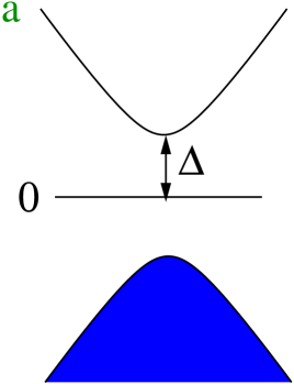
Here is the electron Green’s function and is the RPA Coulomb interaction. First consider the insulator with half band gap shown in Fig. 2a,
with the electron Green’s function
| (2) |
The RPA interaction in this case is the instantaneous Coulomb interaction
| (3) |
Here besided the usual Coulomb repulsion we account three additional points specific for TMD devices. (i) The polarization operator of the zero temperature insulator is practically zero. (ii) Due to the 2D geometry of the system the interaction is described by a Rytova-Keldysh potential, which accounts for differences in the dielectric constant between layers of the system more accurately than the standard 2D Coloumb potential. In this regime there is significant momentum dependence of the effective dielectric constant, , Ref. Cudazzo et al. (2011). (iii) A metallic gate at distance from TMD results in electrostatic screening. Note that both the Green’s function and the interaction are matrices where index corresponds to the positive energy states and corresponds to the negative energy states. The projectors and the unity matrix are
| (10) |
The Green’s function is a diagonal matrix, the interaction in principle has off-diagonal terms, but in TMDs because of the very large band gap eV the wave function overlap between electrons in the conduction and valence bands is vanishingly small and the interaction matrix is thus approximately diagonal. Hence, the electron self energy in the insulator reads
| (11) |
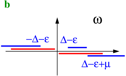
Cuts of this equation integrand in the complex -plane are shown in Fig. 2b. They are determined by the analytical properties of the Green’s function and hence start from and .
The band gap variation due to the interaction is
| (12) |
where superscript () refers to the conduction (valence) band in the insulator. Only the second term in Eq.12 is nonzero. We calculate the gap variation due to finite (relative to )
| (13) | |||||
Let us take MoS2 on SiO2 substrate as an example. For this case we use the following parameters, and nm/, see Refs. Wu et al. (2015); Zhang et al. (2014). We plot band gap renormalization due to gate screening for this device in Fig. 3.
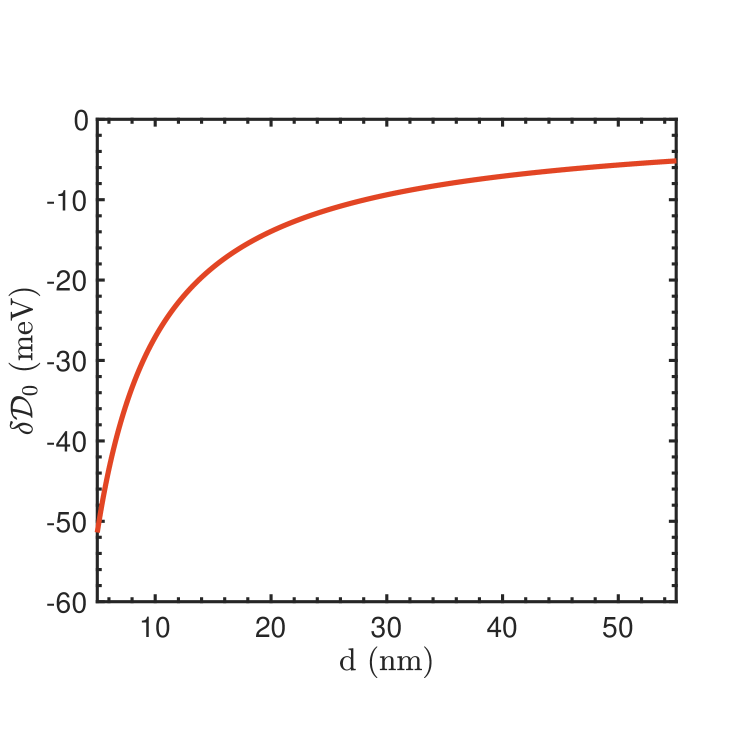
Making speial note of nm, which is typical of such devices, we find gate induced band gap reduction . This effect is non-negligible, but the more significant effect is due to conduction electrons directly in the plane of the 2D TMD. We consider this in the following section.
III Electron Self Energy with conduction electrons, Wick Rotation to Imaginary Axis, the band gap variation
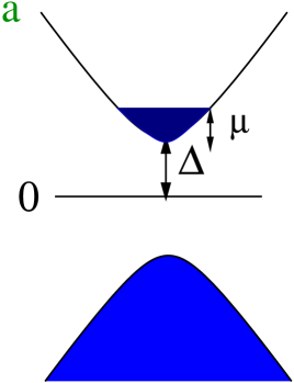
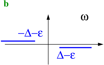
Consider now the metallic regime, where conduction electrons fill the conduction band up to the Fermi level . Filling of states in a metal is shown in Fig. 4a. The RPA interaction in this case is
| (14) |
where is the polarization operator in the metallic state. In the metallic state cuts of the integrand of Eq.(1) in the complex -plane are shown in Fig. 4b. The cuts of the interaction start from , and a part of the Green’s function cut is shifted to the upper half plane due to conduction electrons. This prevents a simple procedure of Wick’s rotation to the imaginary axis as the contour of integration would now cross a branch cut during rotation. To resolve this complication we employ the Sokhotski–Plemelj theorem to represent the Green’s function as
| (15) |
where is the electron occupation number in the conduction (valence) band. Hence the self energy in the metallic state (with ) can be written as
| (16) | |||||
The renormalized self energy operator is the difference between metal, Eq.(16), and insulator, Eq.(11), ,
| (17) | |||||
We stress that we compare the metal and the insulator with the same gate distance . Therefore, the difference at large frequencies, . Hence, the regularizor can be omitted in Eq.(17). After that, having in mind that , the Wick rotation, can be performed in the 1st term of (17). Hence, we arrive at
| (18) | |||||
Similar to Eq.(12) the band gap variation in the metal compared to that in the insulator is , hence
| (19) | |||||
Note that the second term in this equation has a small imaginary part related to the lifetime of a hole at the bottom of the conduction band. The variation of the physical band gap is given by the real part of Eq. (19).
IV Polarization Operator of electrons
In 2D TMDs the band gap is on the order of eV. The Fermi energy of electrons is small compared to the gap, . The polarization operator is entirely due to conduction electrons and is given by the diagram Fig. 5.
The 2D Feynman polarization operator for parabolic dispersion is well known Milstein and Sushkov (2008). In the real frequency formalism it is
| (20) |
Here is the Heaviside step function defined as for , for ; the electron dispersion is . For the imaginary frequency the polarization operator is
| (21) |
The polarization operators (IV),(21) correspond to two electrons per filled momentum state. 2D TMDs have two valleys, but each valley is spin split. This coupling of spin and valley degrees of freedom is well known and is due to strong spin orbit coupling, see Refs. Kormányos et al. (2015); Stier et al. (2016); Rostami et al. (2013); Wang et al. (2018); Scharf et al. (2019). Therefore, there are two different valley/spin states at a given momentum.
V The gap reduction due to conduction electrons
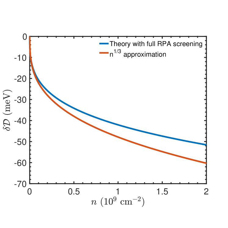
It is important to qualitatively understand the parametric behaviour of the band gap reduction as a function of conduction electron density. There are three parameters of dimension length in Eq.(19), namely the Bohr radius , the dielectric constant momentum dependence scale and the distance to the metallic gate . They are ordered as . With , let be the Fermi momentum of conduction electrons. The most important dimensionless parameter is , which is at cm-2 and at cm-2. Let us first consider the infinitely far gate case, . Analysis of the imaginary frequency integral in (19) shows that it is convergent at . At the length scale may be discarded, which allows for a simple approximate formula in the low density regime cm-2. Although it should be noted that as the small parameter scales with the low density regime is significantly lower than cm-2. In this regime evaluation of integrals in (19) gives
| (22) |
Here the first term comes from the first term in (19) (imaginary frequency integration) and the second term 111Note that in taking the limit the discarding of small terms linear or higher order in leads to the cancellation of terms in the second term of (22), seemingly implying the existence of band gap renormalizaiton in the non-interacting scenario. However, it is clear by inspection of the interaction (III) and Eq. (19) that formally in the limit this term vanishes as required. comes from the second term in (19). Clearly, the first term dominates at low density. While the imaginary part in the second term in Eq. (19) is unrelated to the band gap, still, it is instructive to evaluate it. The imaginary part is .
Again, let us take MoS2 on SiO2 substrate as an example. The relevant parameters are given in Table. 1.
| MoS2. Strata: SiO2, air | ||
|---|---|---|
| Parameter | Value | Description |
| m0 Kormányos et al. (2015) | Effective electron mass | |
| m0 Kormányos et al. (2015) | Effective hole mass | |
| Wu et al. (2015) | Effective dielectric constant | |
| nm/ Wu et al. (2015); Zhang et al. (2014) | Characteristic screening length | |
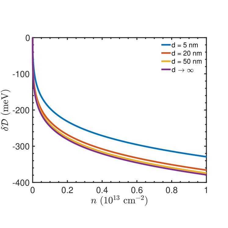
Plots of calculated with the approximation (22) and with exact numerical integration of Eq. (19) with the above set of parameters and are presented in Fig.6, the plots are identical at . In Fig. 7 we present plots of the band gap reduction versus with exact numerical integration of Eq. (19) using the above set of parameters for several values of . This figure clearly demonstrates importance of the gate, which significantly effects at low . We stress that Fig. 7 shows the band gap reduction of the metal compared to the insulator in a set up with the same gate. When comparing two devices with different gate distances the insulator gap reduction relative to the case , given by Eq.(13), must be added on top of this, such that
| (23) |
We remind the reader that is the gap in the insulator with , is the gap in the insulator with finite , and is the correction due to conduction electrons calculated at a given .
The full RPA screening calculations of band gap renormalization performed in this manuscript require careful application of complex analysis techniques. Simplified models have previously been used to account for screening of the Coulomb interaction. In Appendix A we compare our RPA results with a simple static screening model and a plasmon pole model.
VI Comparison With Experimental Data
The intrinsic band gap of 2D TMDs is large compared to the Fermi energy to the extent that the dispersion may be approximated as truly parabolic. Thus when comparing our theory to experimental data 0 may always be tuned independently of .
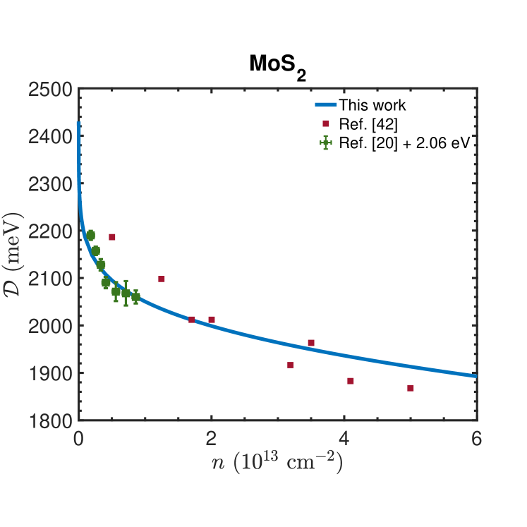
We first consider MoS2 on a SiO2 substrate, with relevant material parameters given in Table 1. Renormalized band gap as a function of n doping calculated from Eq 19 is plotted in Fig. 8. The theoretical prediction is compared with available experimental data from Ref. Liu et al. (2019) and Ref. Yao et al. (2017), where the latter is offset in intrinsic band gap to allow for better comparison of . For the theory curve is set to eV to best fit the data. It is also unclear if there is any initial doping in any of the systems due to impurities. Our theory reasonably agrees with the experimental from Ref. Liu et al. (2019) and is in excellent agreement with Ref. Yao et al. (2017), which captures the dramatic low density reduction.
In both Ref. Liu et al. (2019) and Ref. Yao et al. (2017) the gate is located a distance nm from the 2DEG. Hence according to Eq. 13 the correction is very small, meV, and also can be calculated with , see Fig. 7. Thus in the theoretical calculations presented in Fig. 8 the effects of gate screening are negligible.
| WSe2. Strata: hBN, air | ||
|---|---|---|
| Parameter | Value | Description |
| m0 Kormányos et al. (2015) | Effective electron mass | |
| m0 Nguyen et al. (2019) | Effective hole mass | |
| Nguyen et al. (2019); Engdahl et al. (2024) | Effective dielectric constant | |
| nm/ Engdahl et al. (2024) | Characteristic screening length | |
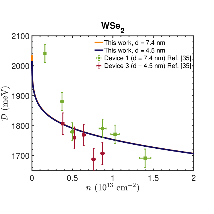
While gate screening effects are negligible in the MoS2 device presented in Fig. 8, the devices from Ref. Nguyen et al. (2019) considered in Fig. 9 feature graphite gates at a distance nm from the 2DEG. In this case the effects of gate screening must be accounted for in both the calculation of band gap renormalization as a function of n doping and the calculation of insulator band gap. In Fig. 9 we present theoretical calculations of vs with a gate located at a distance nm and nm from the 2DEG and superimpose experimental data from Ref. Nguyen et al. (2019). Parameters used in theoretical calculations for the WSe2 device are presented in Table. 2. As the 2DEG and strata are common across the two device we assume the insulating band gap in the limit is the same in both devices, tuning eV. The correction to the insulating band gap is easily calculated with Eq. 13, where meV at nm and meV at nm.
Our theory is in reasonable agreement with the data from Ref. Nguyen et al. (2019), although there is some discrepancy between theory and experimental measurements at low density. It must be noted that in this work we assume the system is free from impurities at and do not account for defects, whereas in reality there may be some level of intrinsic doping, where it is well known within the literature that TMD samples are high in impurities and defects Mueller and Malic (2018); Chaves et al. (2020). Still, the large band gap reduction of meV over the range cm-2 agrees well with the experimental data.
While this manuscript specifically discusses the role of screening from conduction electrons and a metallic gate in band gap renormalization, we point out that a significant renormalization of the band gap may also be caused by variation in dielectric environment. A variation of has experimentally revealed band gap renormalization of around 250 meV for MoSe2 between two different substrates Zhang et al. (2016). For comparison, consider the MoS2 device from Table 1 at constant density cm-2 and . At this density calculated from Eq. 19 is strongly dependent on , with a suspended sample () having a band gap renormalization larger than a sample on a SiO2 substrate () by meV.
VII Summary
We have developed the theory for bandgap renormalization in 2D semiconductors using the Feynman diagrammatic technique traditionally used in QED. In our approach we consider full RPA screening and convert the integral to the imaginary frequency regime which is both analytically and numerically convenient. We derive expressions for band gap renormalization of the insulator due to gate screening, relative to an infinitely far gate, and of the metal due to both screening from conduction electrons and gate screening. Applying our methodology to 2D TMDs, we show the band gap significantly decreases at low density, scaling as . We compare our theoretical predictions with available experimental data for MoS2 and WSe2 and find that our theory is in good agreement with experimental data. This dynamical screening self energy method may be modified and applied to systems with indirect band gaps or systems with a dispersion other than simple parabolic.
VIII Acknowledgements
We acknowledge discussions with Aydın Cem Keser, Zeb Krix, Iolanda Di Bernardo and Shaffique Adam. This work was supported by the Australian Research Council Centre of Excellence in Future Low- Energy Electronics Technologies (CE170100039).
Appendix A Comparison with approximations
Rather than consider the full dynamical screening from RPA, the screened interaction is often approximated with various models with differing levels of success. In this appendix we compare our theory to a static screening model and a plasmon pole model. Note that for simplicity we present solutions for the case .
In the static screening model, rather than considering dynamical screening from the full RPA chain, dynamical effects are ignored and a single value of frequency is used in the determination of the polarization operator in Eq. 17. The interaction no longer has cuts in the complex plane. In this regime the integration is readily solved via simple application of Cauchy’s residue theorem. The total correction to the band gap for the case of static screening is given below in Eq. 24.
| (24) |
Plasmon-pole models are commonly used theoretical models to take dynamical screening into account in the calculation of the quasiparticle band gap in 2D materialsGao et al. (2016); Gao and Yang (2017); Liang and Yang (2015); Qiu et al. (2016). The plasmon pole model involves placing all dynamical screening effects from the dynamical frequency polarization operator on the plasmon-pole and renormalizing the strength of the pole. It is easy to consider the self energy calculation in real frequency and see that plasmon effects dominate the self energy renormalization, thus validating the assumption of the plasmon pole description. We begin by rewriting the difference between the metallic and insulator interaction, where is the plasmon pole strength and is the plasmon frequency which is obtained from a frequency dependent calculation of the poles of the interaction III.
| (25) |
The plasmon pole strength is weighted by the static screening dielectric function.
| (26) |
Substituting 25 into Eq. 17, the cuts of the interaction in the complex plane are replaced by simple poles. Finally, through application of Cauchy’s residue theorem in the complex plane, one may derive an expression for total band gap renormalization in the plasmon pole approximation.
| (27) |
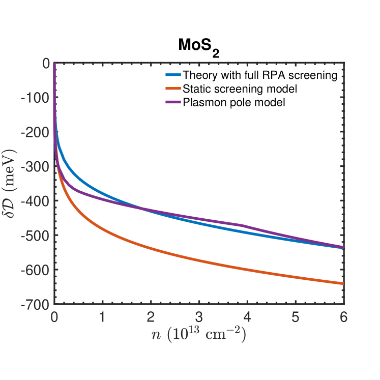
Band gap reduction calculated with the exact expression Eq. 19, the static screening approximation Eq. 24 and the plasmon pole approximation Eq. A are presented in Fig. 10, where the material parameters are taken from Table. 1 and the gate distance is . The plasmon pole model overpredicts for low density cm-2 but is in good agreement with the exact calculation otherwise. Compared with the exact calculation, the static screening model overpredicts by meV at moderate to high carrier density. The cusp in the plasmon pole model is due to the second term in Eq. (A) vanishing, which occurs when the plasmon pole terminates at , ie the plasmon pole exists entirely within the continuum.
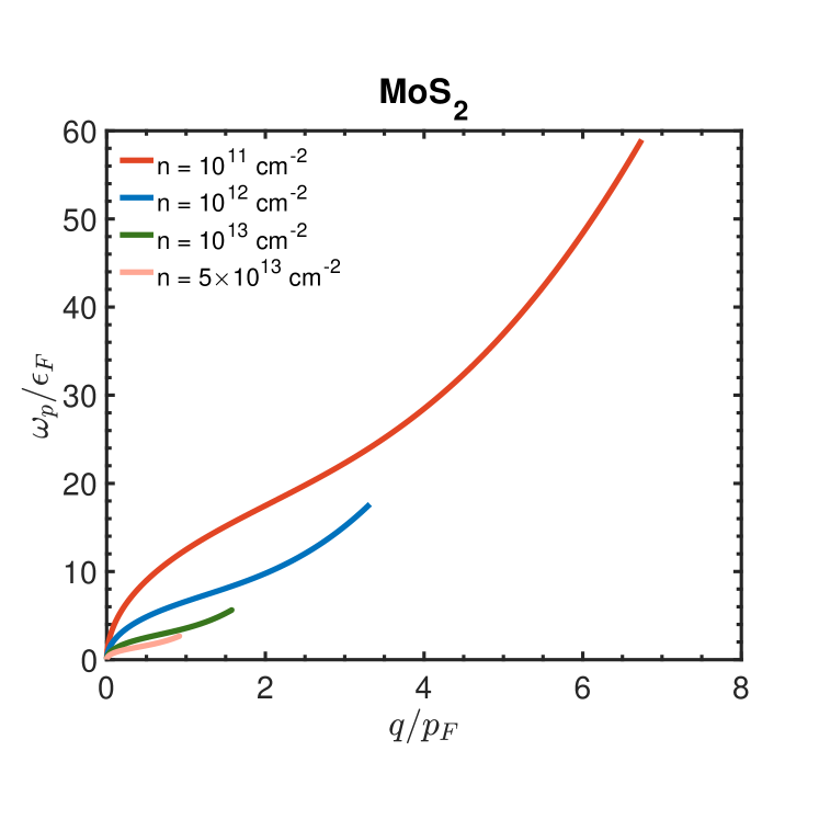
The plasmon pole model used in Fig. 10 uses plasmon frequency that is obtained from a frequency dependent calculation of the RPA screened interaction with the exact plasmon frequency plotted in Fig. 11 as a function of momentum for a number of carrier densities. Clearly plasmons exist up to higher momenta at lower density, therefore contributing more to at low density than at higher density. For the MoS2 device considered, the plasmon frequency exists at momenta until cm-2.
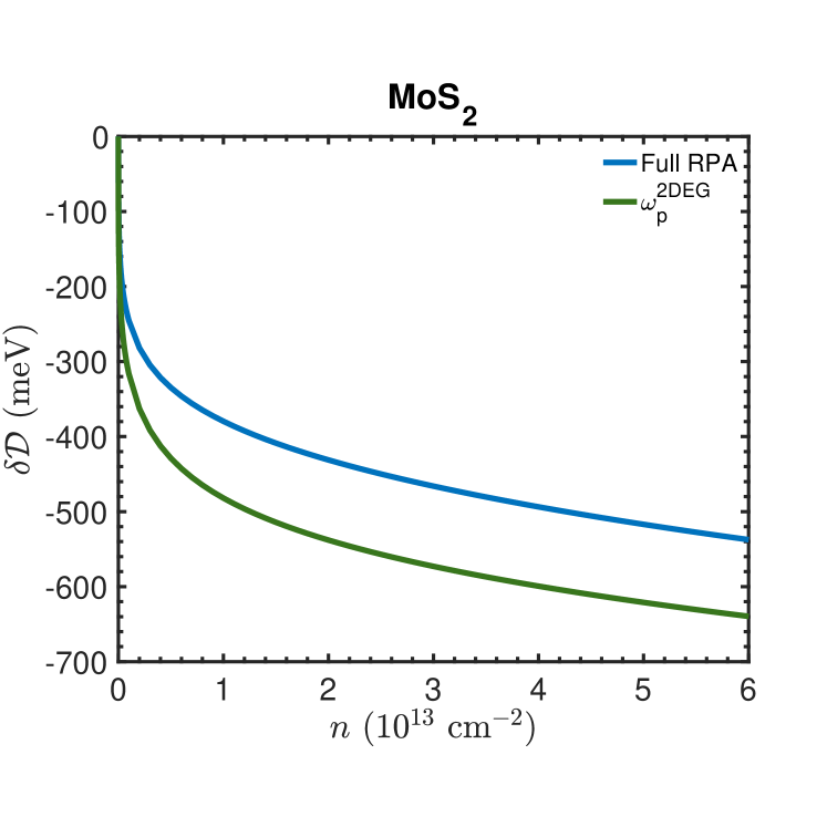
However, the procedure of first exactly determining plasmon frequency is more computationally intensive than computation of the exact calculation in imaginary frequency and for the case of simple parabolic band structure there is little justification for its use. Hence we consider the plasmon pole model where the 2DEG RPA plasmon dispersion relationCzachor et al. (1982)
| (28) |
This allows one to forego the frequency dependent calculation of the RPA screened interaction, however in doing so one neglects the calculation of plasmon termination. Thus this simplified model assumes plasmons exist to infinite momenta. We compare the results of the full RPA calculation with the plasmon pole model using for Mos2 in Fig. 12. In this case the plasmon pole model overpredicts at all , and in fact exactly reproduces the static screening model of Fig. 10. Thus plasmon termination is an important feature of a plasmon pole model that cannot be neglected. In this case there is little justification to using a plasmon pole model over the imaginary frequency full RPA calculation.
References
- Wang et al. (2018) G. Wang, A. Chernikov, M. M. Glazov, T. F. Heinz, X. Marie, T. Amand, and B. Urbaszek, Reviews of Modern Physics 90, 021001 (2018).
- Scharf et al. (2019) B. Scharf, D. Van Tuan, I. Žutić, and H. Dery, Journal of Physics: Condensed Matter 31, 203001 (2019).
- Kormányos et al. (2015) A. Kormányos, G. Burkard, M. Gmitra, J. Fabian, V. Zólyomi, N. D. Drummond, and V. Fal’ko, 2D Materials 2, 022001 (2015).
- Stier et al. (2016) A. V. Stier, K. M. McCreary, B. T. Jonker, J. Kono, and S. A. Crooker, Nature Communications 7, 10643 (2016).
- Rostami et al. (2013) H. Rostami, A. G. Moghaddam, and R. Asgari, Physical Review B 88, 085440 (2013).
- Chen et al. (2019) S.-Y. Chen, Z. Lu, T. Goldstein, J. Tong, A. Chaves, J. Kunstmann, L. S. R. Cavalcante, T. Woźniak, G. Seifert, D. R. Reichman, T. Taniguchi, K. Watanabe, D. Smirnov, and J. Yan, Nano Letters 19, 2464 (2019).
- Wu et al. (2015) F. Wu, F. Qu, and A. H. MacDonald, Physical Review B 91, 075310 (2015).
- Liu et al. (2021) H. Liu, A. Pau, and D. K. Efimkin, Physical Review B 104, 165411 (2021).
- Goldstein et al. (2020) T. Goldstein, Y.-C. Wu, S.-Y. Chen, T. Taniguchi, K. Watanabe, K. Varga, and J. Yan, The Journal of Chemical Physics 153, 071101 (2020).
- Liu et al. (2020) E. Liu, J. Van Baren, T. Taniguchi, K. Watanabe, Y.-C. Chang, and C. H. Lui, Physical Review Letters 124, 097401 (2020).
- Bange et al. (2023) J. P. Bange, P. Werner, D. Schmitt, W. Bennecke, G. Meneghini, A. AlMutairi, M. Merboldt, K. Watanabe, T. Taniguchi, S. Steil, D. Steil, R. T. Weitz, S. Hofmann, G. S. M. Jansen, S. Brem, E. Malic, M. Reutzel, and S. Mathias, 2D Materials 10, 035039 (2023).
- Zhu et al. (2023) B. Zhu, K. Xiao, S. Yang, K. Watanabe, T. Taniguchi, and X. Cui, Physical Review Letters 131, 036901 (2023).
- Meckbach et al. (2018a) L. Meckbach, T. Stroucken, and S. W. Koch, Physical Review B 97, 035425 (2018a).
- Qiu et al. (2016) D. Y. Qiu, F. H. Da Jornada, and S. G. Louie, Physical Review B 93, 235435 (2016).
- Qiu et al. (2019) Z. Qiu, M. Trushin, H. Fang, I. Verzhbitskiy, S. Gao, E. Laksono, M. Yang, P. Lyu, J. Li, J. Su, M. Telychko, K. Watanabe, T. Taniguchi, J. Wu, A. H. C. Neto, L. Yang, G. Eda, S. Adam, and J. Lu, Science Advances 5, eaaw2347 (2019).
- Bera et al. (2021) S. K. Bera, M. Shrivastava, K. Bramhachari, H. Zhang, A. K. Poonia, D. Mandal, E. M. Miller, M. C. Beard, A. Agarwal, and K. V. Adarsh, Physical Review B 104, L201404 (2021).
- Chernikov et al. (2015) A. Chernikov, C. Ruppert, H. M. Hill, A. F. Rigosi, and T. F. Heinz, Nature Photonics 9, 466 (2015).
- Pogna et al. (2016) E. A. A. Pogna, M. Marsili, D. De Fazio, S. Dal Conte, C. Manzoni, D. Sangalli, D. Yoon, A. Lombardo, A. C. Ferrari, A. Marini, G. Cerullo, and D. Prezzi, ACS Nano 10, 1182 (2016).
- Cunningham et al. (2017) P. D. Cunningham, A. T. Hanbicki, K. M. McCreary, and B. T. Jonker, ACS Nano 11, 12601 (2017).
- Yao et al. (2017) K. Yao, A. Yan, S. Kahn, A. Suslu, Y. Liang, E. S. Barnard, S. Tongay, A. Zettl, N. Borys, and P. J. Schuck, Physical Review Letters 119, 087401 (2017).
- Wang et al. (2012) Q. H. Wang, K. Kalantar-Zadeh, A. Kis, J. N. Coleman, and M. S. Strano, Nature Nanotechnology 7, 699 (2012).
- Mueller and Malic (2018) T. Mueller and E. Malic, npj 2D Materials and Applications 2, 29 (2018).
- Taffelli et al. (2021) A. Taffelli, S. Dirè, A. Quaranta, and L. Pancheri, Sensors 21, 2758 (2021).
- Dufferwiel et al. (2018) S. Dufferwiel, T. P. Lyons, D. D. Solnyshkov, A. A. P. Trichet, A. Catanzaro, F. Withers, G. Malpuech, J. M. Smith, K. S. Novoselov, M. S. Skolnick, D. N. Krizhanovskii, and A. I. Tartakovskii, Nature Communications 9, 4797 (2018).
- Zhao et al. (2023) J. Zhao, A. Fieramosca, K. Dini, R. Bao, W. Du, R. Su, Y. Luo, W. Zhao, D. Sanvitto, T. C. H. Liew, and Q. Xiong, Nature Communications 14, 1512 (2023).
- Zhang et al. (2020) Q. Zhang, S. Dong, G. Cao, and G. Hu, Optics Letters 45, 4140 (2020).
- Yin et al. (2012) Z. Yin, H. Li, H. Li, L. Jiang, Y. Shi, Y. Sun, G. Lu, Q. Zhang, X. Chen, and H. Zhang, ACS Nano 6, 74 (2012).
- Velusamy et al. (2015) D. B. Velusamy, R. H. Kim, S. Cha, J. Huh, R. Khazaeinezhad, S. H. Kassani, G. Song, S. M. Cho, S. H. Cho, I. Hwang, J. Lee, K. Oh, H. Choi, and C. Park, Nature Communications 6, 8063 (2015).
- Chang et al. (2014) Y.-H. Chang, W. Zhang, Y. Zhu, Y. Han, J. Pu, J.-K. Chang, W.-T. Hsu, J.-K. Huang, C.-L. Hsu, M.-H. Chiu, T. Takenobu, H. Li, C.-I. Wu, W.-H. Chang, A. T. S. Wee, and L.-J. Li, ACS Nano 8, 8582 (2014).
- Zhang et al. (2013) W. Zhang, J. Huang, C. Chen, Y. Chang, Y. Cheng, and L. Li, Advanced Materials 25, 3456 (2013).
- Lopez-Sanchez et al. (2013) O. Lopez-Sanchez, D. Lembke, M. Kayci, A. Radenovic, and A. Kis, Nature Nanotechnology 8, 497 (2013).
- Gonzalez Marin et al. (2019) J. F. Gonzalez Marin, D. Unuchek, K. Watanabe, T. Taniguchi, and A. Kis, npj 2D Materials and Applications 3, 14 (2019).
- Lee et al. (2021) W. Lee, Y. Lin, L.-S. Lu, W.-C. Chueh, M. Liu, X. Li, W.-H. Chang, R. A. Kaindl, and C.-K. Shih, Nano Letters 21, 7363 (2021).
- Kang et al. (2017) M. Kang, B. Kim, S. H. Ryu, S. W. Jung, J. Kim, L. Moreschini, C. Jozwiak, E. Rotenberg, A. Bostwick, and K. S. Kim, Nano Letters 17, 1610 (2017).
- Nguyen et al. (2019) P. V. Nguyen, N. C. Teutsch, N. P. Wilson, J. Kahn, X. Xia, A. J. Graham, V. Kandyba, A. Giampietri, A. Barinov, G. C. Constantinescu, N. Yeung, N. D. M. Hine, X. Xu, D. H. Cobden, and N. R. Wilson, Nature 572, 220 (2019).
- Zhang et al. (2016) Q. Zhang, Y. Chen, C. Zhang, C.-R. Pan, M.-Y. Chou, C. Zeng, and C.-K. Shih, Nature Communications 7, 13843 (2016).
- Gao et al. (2016) S. Gao, Y. Liang, C. D. Spataru, and L. Yang, Nano Letters 16, 5568 (2016).
- Karmakar et al. (2021) M. Karmakar, S. Bhattacharya, S. Mukherjee, B. Ghosh, R. K. Chowdhury, A. Agarwal, S. K. Ray, D. Chanda, and P. K. Datta, Physical Review B 103, 075437 (2021).
- Steinhoff et al. (2018) A. Steinhoff, T. O. Wehling, and M. Rösner, Physical Review B 98, 045304 (2018).
- Liang and Yang (2015) Y. Liang and L. Yang, Physical Review Letters 114, 063001 (2015).
- Zibouche et al. (2021) N. Zibouche, M. Schlipf, and F. Giustino, Physical Review B 103, 125401 (2021).
- Liu et al. (2019) F. Liu, M. E. Ziffer, K. R. Hansen, J. Wang, and X. Zhu, Physical Review Letters 122, 246803 (2019).
- Ataei and Sadeghi (2021) S. S. Ataei and A. Sadeghi, Physical Review B 104, 155301 (2021).
- Fernández et al. (2020) L. Fernández, V. S. Alves, L. O. Nascimento, F. Peña, M. Gomes, and E. Marino, Physical Review D 102, 016020 (2020).
- Meckbach et al. (2018b) L. Meckbach, T. Stroucken, and S. W. Koch, Applied Physics Letters 112, 061104 (2018b).
- Tian et al. (2022) X. Tian, R. Wei, Z. Ma, and J. Qiu, ACS Applied Materials & Interfaces 14, 8274 (2022).
- Wood et al. (2020) R. E. Wood, L. T. Lloyd, F. Mujid, L. Wang, M. A. Allodi, H. Gao, R. Mazuski, P.-C. Ting, S. Xie, J. Park, and G. S. Engel, The Journal of Physical Chemistry Letters 11, 2658 (2020).
- Beresteckii et al. (2008) V. B. Beresteckii, E. M. Lifshitz, and L. P. Pitaevskii, Quantum electrodynamics, 2nd ed., Course of theoretical physics / L. D. Landau and E. M. Lifshitz No. 4 (Butterworth-Heinemann, Oxford, 2008).
- Gao and Yang (2017) S. Gao and L. Yang, Physical Review B 96, 155410 (2017).
- Faridi et al. (2021) A. Faridi, D. Culcer, and R. Asgari, Physical Review B 104, 085432 (2021).
- Cudazzo et al. (2011) P. Cudazzo, I. V. Tokatly, and A. Rubio, Physical Review B 84, 085406 (2011).
- Zhang et al. (2014) C. Zhang, H. Wang, W. Chan, C. Manolatou, and F. Rana, Physical Review B 89, 205436 (2014).
- Milstein and Sushkov (2008) A. I. Milstein and O. P. Sushkov, Physical Review B 78, 014501 (2008).
- Note (1) Note that in taking the limit the discarding of small terms linear or higher order in leads to the cancellation of terms in the second term of (22), seemingly implying the existence of band gap renormalizaiton in the non-interacting scenario. However, it is clear by inspection of the interaction (III) and Eq. (19) that formally in the limit this term vanishes as required.
- Engdahl et al. (2024) J. N. Engdahl, H. D. Scammell, D. K. Efimkin, and O. P. Sushkov, (2024), 10.48550/ARXIV.2409.18373, version Number: 1.
- Chaves et al. (2020) A. Chaves, J. G. Azadani, H. Alsalman, D. R. Da Costa, R. Frisenda, A. J. Chaves, S. H. Song, Y. D. Kim, D. He, J. Zhou, A. Castellanos-Gomez, F. M. Peeters, Z. Liu, C. L. Hinkle, S.-H. Oh, P. D. Ye, S. J. Koester, Y. H. Lee, P. Avouris, X. Wang, and T. Low, npj 2D Materials and Applications 4, 29 (2020).
- Czachor et al. (1982) A. Czachor, A. Holas, S. R. Sharma, and K. S. Singwi, Physical Review B 25, 2144 (1982).