XXXX-XXXX
1]Department of Physics, Graduate School of Science, Tohoku University, Sendai 980-8578, Japan 2]Department of Physics, Graduate School of Science, Kyoto University, Kyoto 606-8502, Japan 3]International Center for Elementary Particle Physics, University of Tokyo, Tokyo, 113-0033, Japan 4]Institute for Integrated Radiation and Nuclear Science, Kyoto University, Kumatori 590-0494, Japan 5]High Energy Accelerator Research Organization (KEK), Tsukuba 305-0801, Japan 6]Department of Physics, Graduate School of Science, University of Tokyo, Tokyo, 113-0033, Japan 7]Research Center for Neutrino Science, Frontier Research Institute for Interdisciplinary Sciences, Tohoku University, Sendai, 980-8578, Japan 8]Kamioka Observatory, Institute for Cosmic Ray Research, The University of Tokyo, Hida, 506-1205, Japan 9]Kavli Institute for the Physics and Mathematics of the Universe, The University of Tokyo, Kashiwa, 277-8583, Japan
In-situ high voltage generation with Cockcroft-Walton multiplier for xenon gas time projection chamber
Abstract
We have newly developed a Cockcroft-Walton (CW) multiplier that can be used in a gas time projection chamber (TPC). TPC requires a high voltage to form an electric field that drifts ionization electrons. Supplying the high voltage from outside the pressure vessel requires a dedicated high-voltage feedthrough. An alternative approach is to generate the high voltage inside the pressure vessel with a relatively low voltage introduced from outside. CW multiplier can convert a low AC voltage input to a high DC voltage output, making it suitable for this purpose.
We have integrated the CW multiplier into a high-pressure xenon gas TPC, called AXEL (A Xenon ElectroLuminescence detector), which have been developed to search for neutrinoless double beta decay of 136Xe. It detects ionization electrons by detecting electroluminescence with silicon photomultipliers, making it strong against electrical noises. An operation with the CW multiplier was successfully demonstrated; the TPC was operated for 77 days at , and an energy resolution as high as (FWHM) at was obtained.
H20
1 Introduction
Neutrinoless double beta decay () is a phenomenon in which two beta decays occur simultaneously and the neutrinos annihilate each other virtually, resulting in the emission of only two electrons. This phenomenon occurs when neutrinos have a Majorana nature, and, even if happens, it would be a very rare decayPhysRev.56.1184 . So far, it has never been observed. One of the candidate parent nuclide is 136Xe, for which the KamLAND-ZEN experiment has given the most stringent lower limit of the half-life: years (90% C.L.)PhysRevLett.130.051801 . The corresponding upper limit on the effective Majorana neutrino mass is in the range 36-156 meV. In order to conduct experiments with higher sensitivity, a ton-scale detector with higher energy resolution, and lower background is required. High-pressure xenon gas time projection chamber (TPC) is a candidate detector that fulfills these requirements. However, there are also technical challenges. One such challenge is related to the high voltage to generate a electric field to guide ionization electrons to the detection surface. For a gas TPC, the required voltage is higher than . To feed such high voltage (HV) from outside the pressure vessel, high voltage feedthroughs compatible with high pressures are needed. Another approach is to introduce a relatively low voltage from outside the pressure vessel and boost it inside the pressure vessel. The Cockcroft-Walton (CW) multiplierdoi:10.1098/rspa.1932.0107 can be used to convert a low voltage AC input to a high voltage DC output. This approach was proposed for liquid argon TPC’sMarchionni_2011 , but has not been realized in actual operation. One difficulty comes from the noise caused by the AC input. If the AC input is turned off after charging the capacitors in the CW multiplier, the noise disappears but it becomes uncertain if the voltage is properly maintained.
We are developing a high pressure xenon gas TPC called AXEL, A Xenon ElectroLuminescence detector. We use the electroluminescence (EL) process as a signal: electrons accelerated by an electric field excite atoms, and photons are emitted as a result of the de-excitation. The idea of using the EL process in a high-pressure gas TPC’s to achieve high energy resolution and tracking performance are first proposed and adopted by NEXT experiment4437191 VÁlvarez_2013 , and search has already been conductedNovella2023 . Since the charge is converted to light and read out, it is highly resistant to electrical noise. We have developed a CW multiplier to supply high voltage to the AXEL detector10.1093/ptep/ptad146 and installed it into the prototype detector. The performance was evaluated at -ray peak from , through long-term measurements. This paper reports the developed CW multiplier, and the performance of the TPC equipped with it.
2 AXEL detector
The schematic view of the AXEL prototype detector is shown in Fig. 1.
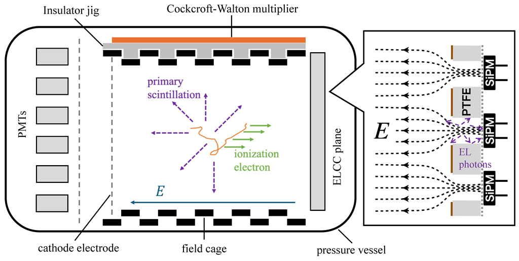
As a charged particle passes through the gas volume of the detector, it excites and ionizes xenon atoms along the track. The excited atoms results in emissions of the primary scintillation light, which are detected with photomultiplier tubes (PMTs). This signal is used as the timing of the event. Ionization electrons drift along the uniform drift electric field formed by a field cage toward the detection plane called ELCC, and enter into each cell of ELCC along the electric field line. Inside the cell, electrons are accelerated by a stronger electric field and excites xenon atoms. Then, de-excitation results in the emission of EL photons. The EL photons are detected with a Silicon Photomultiplier (SiPM) located on the back of the ELCC. The time for ionization electrons to drift through the chamber is on the order of time scale, whereas the scintillation light is sufficiently short . This readout in each cell of the ELCC with time information allows reconstruction of the 3D track. The number of detected photons at each timing and cell position gives the energy deposit of the corresponding position on the track. The total number of photons gives the total energy of the track. Detailed configuration of the AXEL detector is described in a previous work10.1093/ptep/ptad146 . In the following, we describe the ELCC and field cages in detail, which were updated from the previous work.
2.1 ELCC
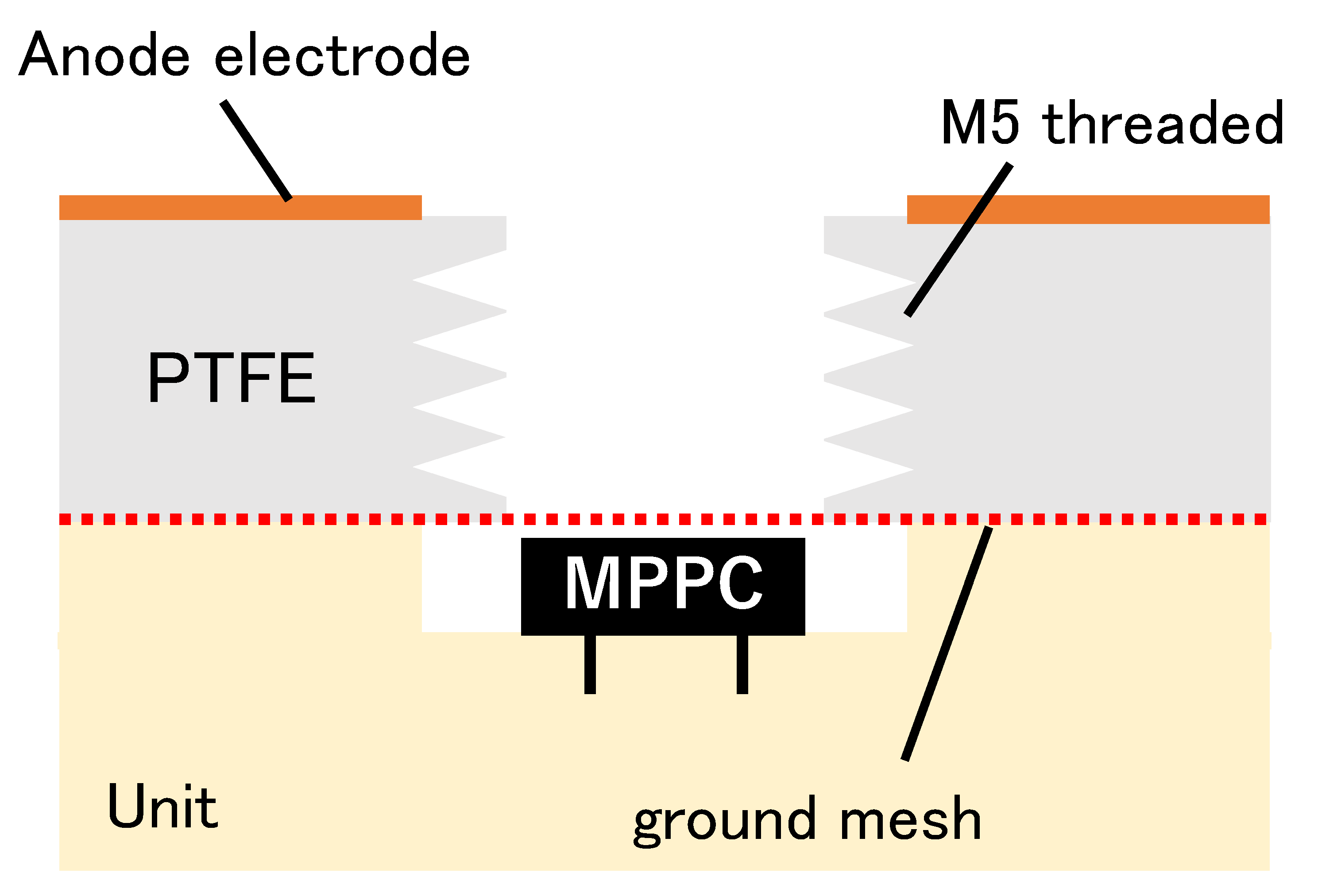
Electroluminescence light collection cell, ELCC, is an ionization-electron detection device utilizing the EL process. ELCC consists of the TPC anode and ground mesh electrodes, with a 5mm-thick PTFE plate between them. The plate has round holes arranged in a hexagonal pattern at intervals, as the cells. The inside the cell is subjected to an electric field of by the voltage difference between the anode and ground electrodes, with which EL process is induced by the ionization electrons. ELCC consists of multiple units of a same structure. A single unit is composed of cells. Vacuum ultraviolet (VUV) photons emitted by the EL process in a cell are detected by multi-pixel photon counters (MPPCs), a Hamamatsu VUV sensitive S13370-3050CN silicon photomultiplier located behind the ground mesh.
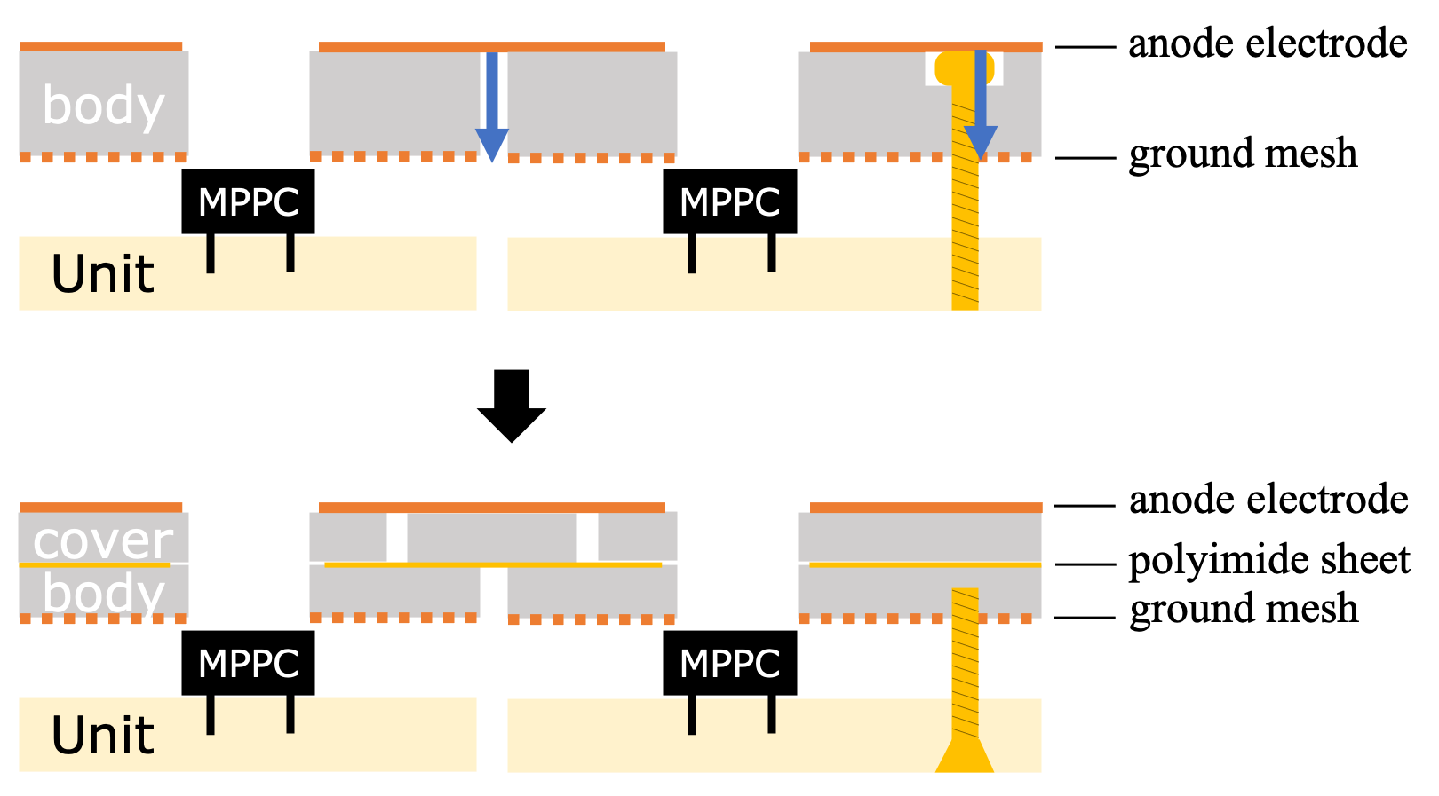
The target value of the field strength in the cell is but has not been achieved due to discharges between the anode and ground electrodes. In the previous study, discharge occurred between the anode and the ground mesh electrodes at the boundaries of the ELCC units and at the screw holes to fix the ELCC units. As a countermeasure against these discharges, the PTFE plate was divided into two layers; a cover layer was added to cover the gaps between units. Also, the screws fixing ELCCs were modified so that they do not penetrate the PTFE plate. Figure 2 left shows these modifications. However, electrical discharges had still occurred, so additional countermeasures are applied in this study. The two-layer structure in the previous study showed discharges presumably on the surface of the polyimide sheet sandwiched between the layers. Therefore, polyimide sheets are not used, and the two-layer structure is employed only at the perimeter cells of the unit. In addition, to prevent discharge along the holes of the cell, the holes are tapped with the JIS M5 threads as shown in Fig. 2 right.
2.2 Field cage
The field cage is a frame for creating a uniform electric field that guides ionization electrons to the detection plane. The field cage of the prototype consists of two types of circular bands with diameters and , arranged alternately with a pitch. This circular electrode is flattened in one part to allow the CW multiplier to be placed in the gap between the chamber and the electrode. A thick high-density polyethylene (HDPE) tube is inserted between the field cage and the chamber for insulation. The topmost electrode is a cathode electrode with a mesh to allow scintillation light to pass through and prevent leakage of the electric field. The number of electrodes was increased from 18 to 40 in order to expand the sensitive volume. First 20 bands are made of thick aluminum and rest is made of thick copper. Aluminum was adopted for a cost reason. The voltage to the cathode electrode was applied by a CW multiplier described in Sec. 3.
3 Design and performance of Cockcroft-Walton multiplier
3.1 Requirement
The schematic diagram of the CW multiplier is shown in Fig.3.

The CW multiplier is composed of multiple stages of a basic circuit, consisting of two capacitors and two diodes, connected in series. The ideal output voltage of an -stage CW multiplier is given as , where is the amplitude of the AC input voltage, but the output voltage of a CW multiplier is actually lower than ideal voltage due to the parasitic capacitance of diodes and load resistance10.1063/1.1683930 .
The AXEL experiment aims to apply a drift electric field of above for ELCC in xenon at 8 bar. To install a CW multiplier inside the chamber, there are several requirements regarding size and material. The CW multiplier is installed in a narrow space between the HDPE tube and the field cage. In case of the prototype, the width is limited to about , height to a few centimeters, the length to to fit to the length of the field cage, and the target voltage is .
It has to be composed of low outgassing materials. This is because impurities with high electronegativity, such as oxygen, adsorb ionization electrons, reducing the TPC signal and degrading the energy resolution. The typical outgassing rate of the prototype detector is , with which xenon gas purity is kept sufficiently high by continuous purification using a molecular sieve and a getter. The outgassing of the CW multiplier should be well below this rate.
3.2 Components
To realize small dimensions and reduce outgassing, we have adopted a flexible printed circuit (FPC) board with surface-mount devices on it. The FPC consists of an -thick copper electrode sandwiched between a -thick polyimide base and coverlay. One board is long and contains 10 CW stages, and a resistor chain to evenly divide the electrical potential to the electrodes of the field cage. The circuit has C-shaped electrodes at both ends, allowing to be connected to each other (Fig. 4).
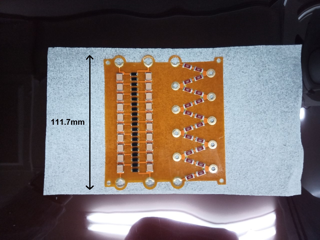
This enables the construction of a CW circuit with more stages. The fewer the number of CW stages, the more efficient the voltage boost, but the higher the voltage applied to the element per stage. Since the rated voltage of the elements is , the circuit was set up with 10 stages per board. When the rated voltage is applied, the required voltage can be achieved with an efficiency of about .
We used a Knowles Syfer’s 2220 chip size ceramic capacitor. For a diode, we used fast switching diode Micro Commercial Components FM2000GP with a reverse recovery time of and typical junction capacitance of . For resistance chains, Bourns Inc. CHV2512-JW-107ELF is used. The rated voltage of these elements is .
3.3 High voltage generation
The voltage drop due to the load resistance is suppressed with higher input frequency. We measured frequency dependence of the output voltage, with a setup shown in Fig. 5.


To feed the AC input power to the CW multiplier, a sine wave from a function generator GW Instek AFG-2005v was amplified by an AC amplifier Matsusada HJOPS-2B10. The maximum output voltage and current of the AC amplifier is , respectively. The slew rate is and bandwidth is (). The output of the CW multiplier was connected to the ground through a resistor chain on the boards and an ammeter Agilent Technologies U3401A. The output voltage is obtained from the measured current value as . Here the resistance value is per 10 steps of the resistor chain on the boards.
The measurement was done with various number of boards, and the results are shown in Fig. 6. Although the prepared CW multiplier initially consisted of seven boards, measurements were conducted with only five boards due to the exclusion of those that experienced discharge during testing.
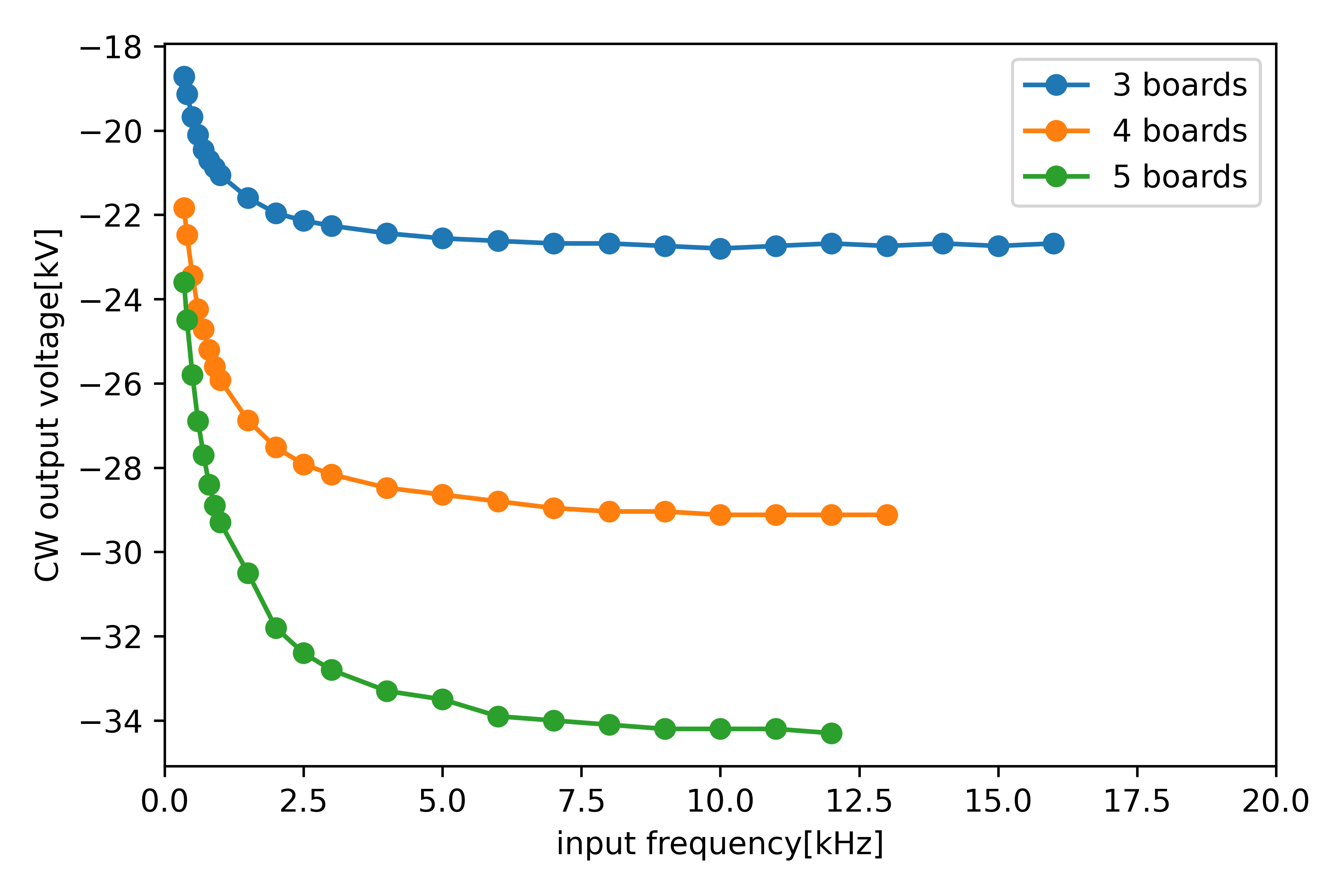
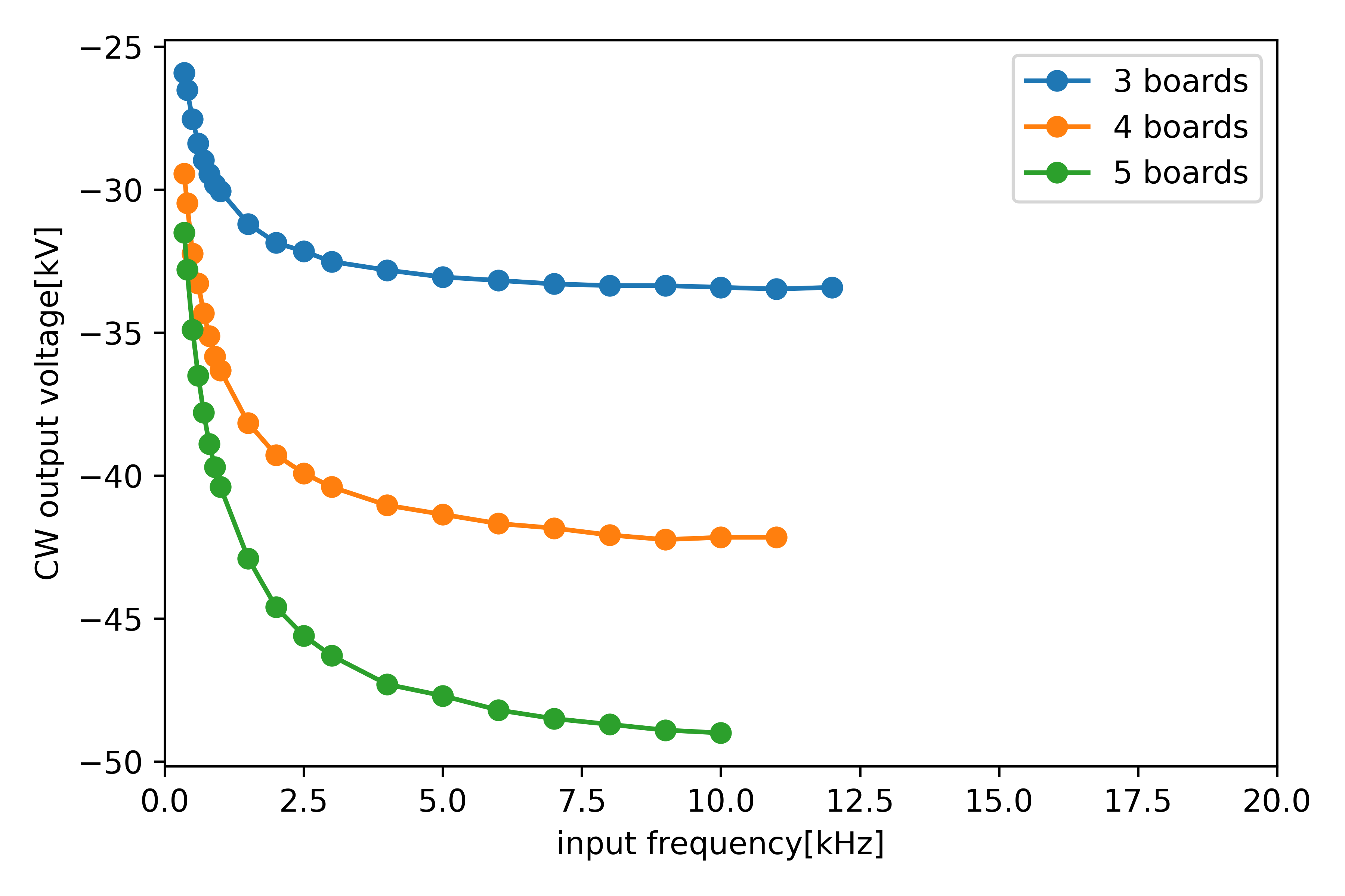
The input peak-to-peak voltages are and . The data points are missing on the high-frequency side. This is because the output voltage of the amplifier became unstable due to the oscillation. The output of the amplifier becomes unstable at lower frequency with more boards. This is thought to be due to the increase in capacitive load with more boards, which leads to the amplifier’s output current reaching its limit. We have confirmed that the operation at higher frequencies is possible by using a higher power audio amplifier and transformer, and we plan to introduce this in the future.
3.4 Surface insulation
During the test operation of the CW multiplier at the peak-to-peak input, surface discharge occurred on the capacitor and FPC surface and the output voltage of the CW multiplier deteriorated. Therefore, we coated the circuit with a methyl silicone resin, Shin-Etsu Chemical Co. Ltd. KR-251 to improve the withstand voltage. The coating is applied by the following procedure.
-
1.
Ultrasonically clean the circuit in ethanol for 15 minutes.
-
2.
Submerge the circuit in a vat containing KR-251 and run it through ultrasonic cleaning for 15 minutes to defoam.
-
3.
Degas the circuit under vacuum for one hour while submerged in KR-251.
-
4.
Lift the circuit out of the KR-251 bath and dry it in a vacuum for 4 hours.
Even with the above procedure, air bubbles around the circuit elements could not be completely removed. To estimate the impact of outgassing from these bubbles on gas purity, we measured the outgassing rate of a coated FPC.
3.5 Outgas rate
A vacuum test was performed using about of a coated circuit piece. The circuit piece was placed in a NW50 pipe connected to a turbo molecular pump, evacuated for about 5 days. The outgassing rate was estimated from the pressure rise as a function of time after shut out from the pump. The pressure changed from to over about 14 hours. The estimated outgassing rate is including leaks in the vacuum system. Since the prototype detector uses four circuit sheets, the outgassing is estimated to be , which is about an order of magnitude less than the typical operational outgassing rate.
3.6 Monitoring of output voltage for the prototype detector
Figure 7 shows the schematic diagram of the HV supplies to the prototype detector.

When operating with the prototype detector, the CW output voltage is monitored with the voltage and current of the Anode DC power supply. A Matsusada HFR10-20N DC power supply is used to apply the TPC anode voltage to the ELCC surface. This power supply has the monitoring output for voltage and current and they are used to estimate the CW output voltage.
The anode and cathode are subject to negative voltages, and , respectively. The output voltage of the CW multiplier is given by,
| (1) |
Here, is an additional load resister for the anode power supply, which is , and is the resistance of the entire TPC resistance chain, which is .
4 Operation as a HV supplier to the 180L detector
Four CW multiplier and resistor chain boards were connected and fixed on a PTFE plate and installed on the flat surface of the field cage, as shown in Fig. 8. To prevent electrical discharges, 2 grooves were made on the surface every of the plate.

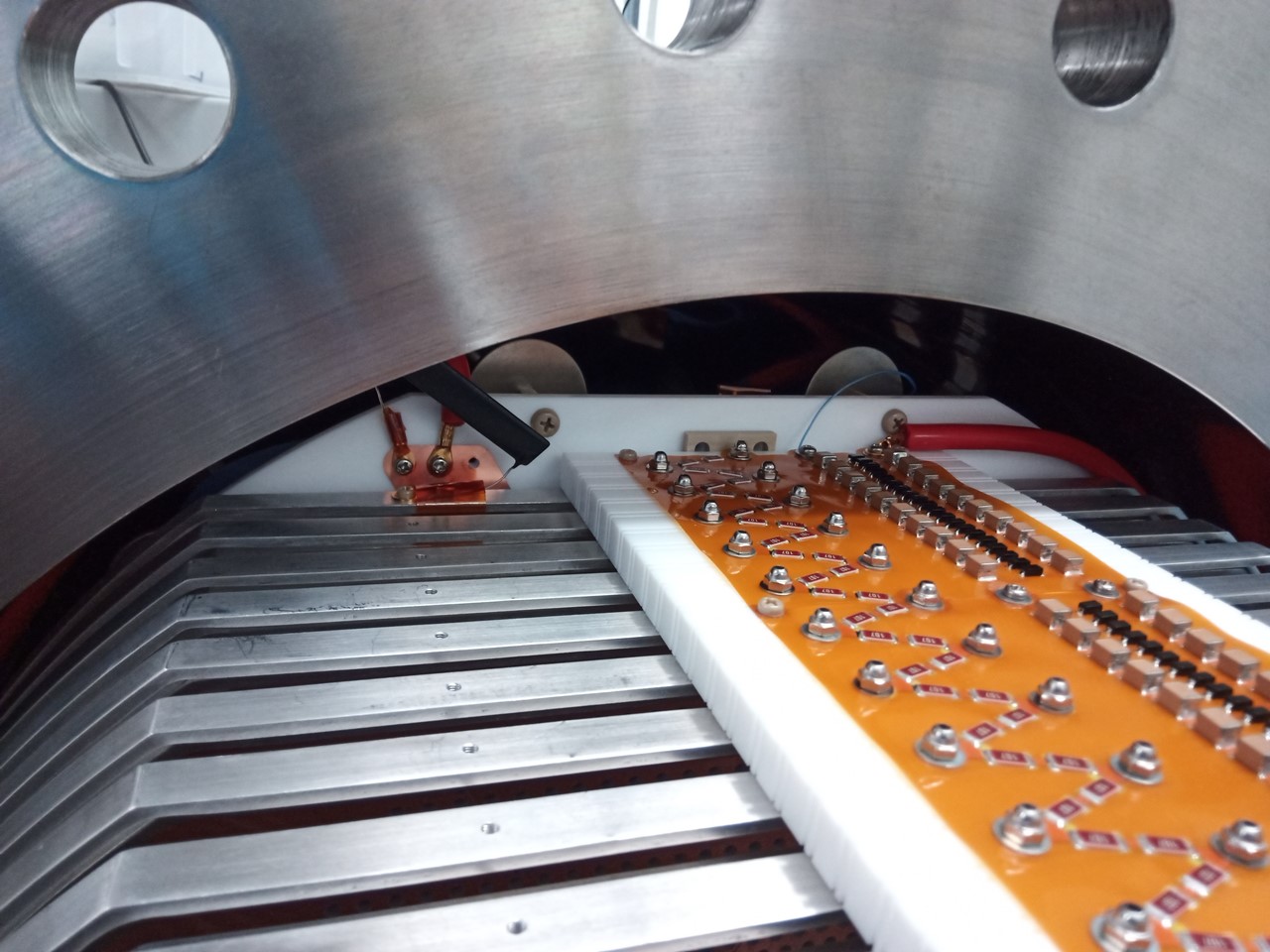
A stainless steel screw connects each electrode of the field cage and each stage of the resistor chain on the boards. Although it is preferable to use coaxial cables to suppress the leak of the electrical noise, a silicon-rubber insulated single-wire cable was used for the input to the CW multiplier, because the use of coaxial cables causes oscillation of the AC amplifier due to the capacitive load of the cable.
The chamber was evacuated for about 5 days before introducing xenon gas. The pressure reached to and the outgassing rate was . Then, xenon gas was filled to about . Data acquisition started after 9 days of gas purification by a molecular sieve and a getter, and continued for 77 days including intervals.
The applied high voltage was raised gradually, but a discharge happend before reaching to the target value of for . Therefore, the data-taking was conducted at the of the design value, , which gives a drift electric field. The applied voltage to ELCC was also set at the of the design value, too. The applied voltages were hence for the anode and for the cathode. From the later inspection of the discharge tracks, it was inferred that the charge flow from the cathode electrode and headed via the inner surface of the HDPE tube to the chamber.
A sample waveform of an ELCC channel without hits during data acquisition is shown in Fig 9.
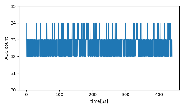
The applied AC frequency of the CW multiplier is and the corresponding cycle is . The baseline is stable within 1 to 2 ADC counts. The distribution of the baseline standard deviations for all the ELCC channels is shown in Fig. 10.
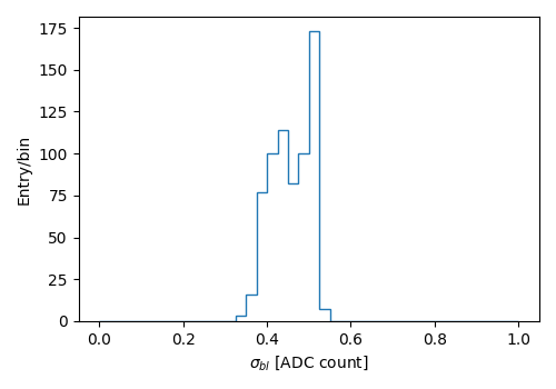
The mean standard deviation is 0.46, while 0.45 when measured without high voltage applied. The effect of baseline fluctuations within one ADC count on the energy resolution is small enough compared to other factors. Therefore, the effect of electrical noise due to the CW multiplier is not a problem.
We used thorium-doped tungsten rods as a gamma-ray source. This is a commercial product for welding and contains thorium and hence contains in the thorium series. A nucleus emits a gamma ray of , which is close to the energy of -rays from the , . The amount of source used is at the beginning and later doubled. The intensity is and respectively.
One row on the outer edge of the ELCC was used as a veto channel to select fully contained event. There were two dead channels and two high dark current channels (see Fig. 11).

These channels were set as veto, and for the dead channel, the surrounding 1 cell was also set as a veto channel.
Various monitored quantities during the data taking period are shown in Fig. 12.

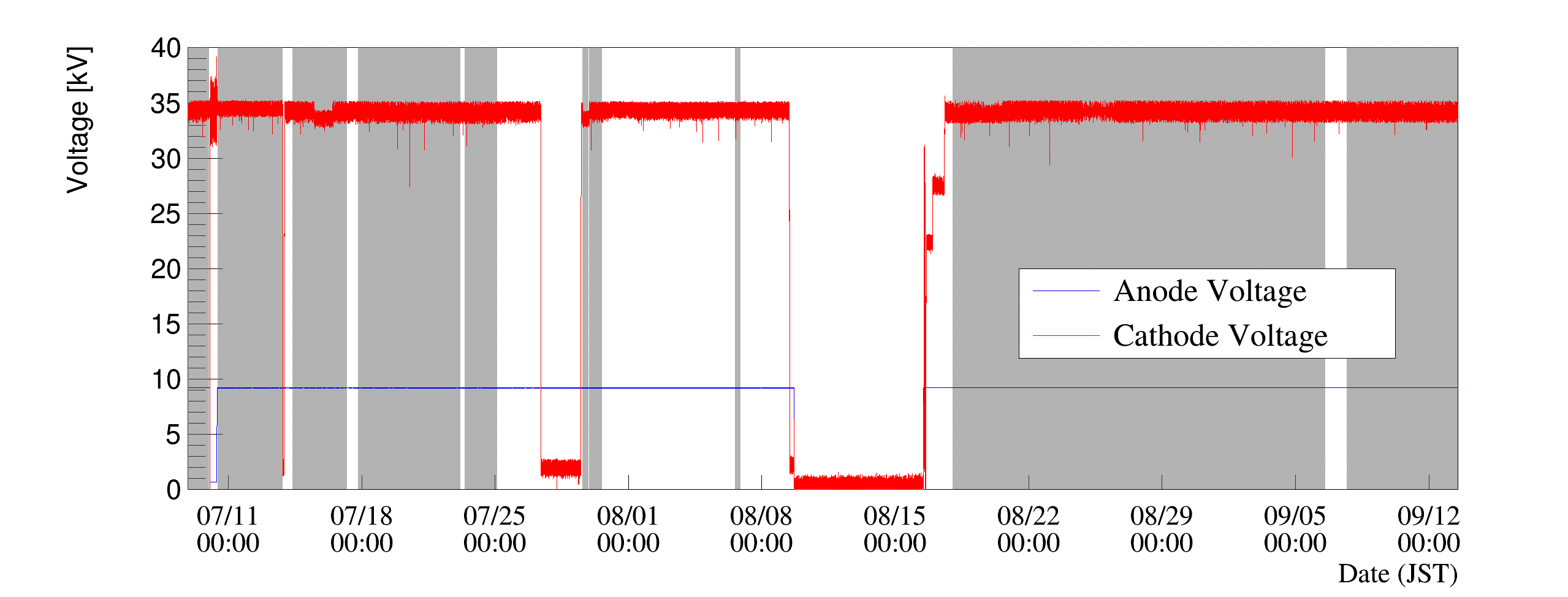
The CW output voltage has a time variation of about and can drop several kV momentarily. As an example, the CW output voltage, anode current, and anode voltage on July 20 are shown in Fig. 13.

The CW output voltage fluctuates at during this period. As can be seen from Eq. 1, the CW output voltage is estimated from and . While the anode voltage remains sufficiently stable, the variation in the CW output voltage is primarily dependent on the fluctuations in anode current. Around 12 noon, an instantaneous voltage drop of about occurs, likely due to a temporary increase in anode current caused by discharge in the CW and ELCC. The frequency of this momentary voltage drop was less than a few times per day and did not cause DAQ outages. On July 27, the CW output voltage drops to about 2 kV. This is because the voltage input to the CW multiplier was stopped due to an interlock caused by a discharge. The anode voltage of remained applied, and the voltage drop in the resistor chain was probably caused by reverse current flow through the diodes in the CW multiplier. Moisture content was also monitored using a dew point meter and was below the lower limit of the meter for most of the measurement period. This means that the moisture content was less than 0.05 ppm.
There are two kinds of triggers, the fiducial trigger and the whole trigger, for the data acquisition of the ELCC signal10.1093/ptep/ptad146 . For this measurement, the threshold of the fiducial trigger was set to about and the whole trigger to slightly above the baseline. To reduce data volume, the whole trigger was set to retrieve only once per events.
5 Analysis
We used data taken from July 8, 2024 to September 13, 2024 when trigger conditions were finalized and stable operation was possible, for the analysis. Here, we briefly describe the method for estimating the energy of each event from the obtained data. For a detailed description of the analysis method, see 10.1093/ptep/ptad146 .
5.1 ELCC waveform analysis
From the waveform of each ELCC channel, hits are identified with a certain threshold from the baseline. Photon counts of each hit is calculated using the MPPC gain, where the MPPC nonlinearity is also corrected11.1093/ptep/ptaa030 . Hits form clusters by grouping those that are spatially and temporally adjacent for each event.
Photon count of each cluster or each event is obtained by summing up those of hits after the gain of the EL process in each ELCC cell (hereafter, EL gain) is corrected. The EL gain is defined as the average detected photon count for one ionization electron. The EL gains are different cell-by-cell due to machinning inaccuracy and photon detection efficiency differences of MPPC’s. To determine the correction factor, peaks of characteristic X-ray () clusters detected during the measurement are used.
The average EL gain in this measurement was found to be 11.5, which is smaller than the 12.5 in the previous study10.1093/ptep/ptad146 . This is presumably due to the tapped hole processing of the ELCC cell, which reduced the light detection efficiency by the MPPC’s.
5.2 PMT waveform analysis
To select primary scintillation photon candidates, hits are detected from the PMT waveform with a certain threshold from baseline. Because hits include EL light leaking from ELCC cells as well as primary scintillation light, hits with a width of less than and at least away from other hits are selected. Of these hits, when two or more channels have hits within , they are considered as primary scintillation light hit clusters. Events with multiple clusters are rejected. The distribution of the time intervals between the primary scintillation and the end of the ELCC signal is shown in Fig. 14.
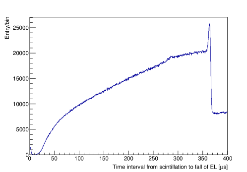
The peak at is formed by the events crossing the cathode of the field cage, for this measurement, . From this, the drift velocity of ionization electrons is derived to be . The z-positions of ELCC hits are reconstructed using this drift velocity.
There are additional selections to avoid timing mismatches, see the previous study10.1093/ptep/ptad146 for details.
5.3 Fiducial volume cut and overall corrections
Using the information from ELCC and PMT, an additional fiducial volume cut is applied. Small photon count clusters due to a few electrons are eliminated from events. These electrons are considered to be produced by the photoelectric effect caused by EL light or by the release of electrons attached to impurities. Fully contained events are selected by rejecting events with hits in the veto channel and restricting the z-position to the region. Then, following overall corrections were applied.
5.3.1 Correction of time variation
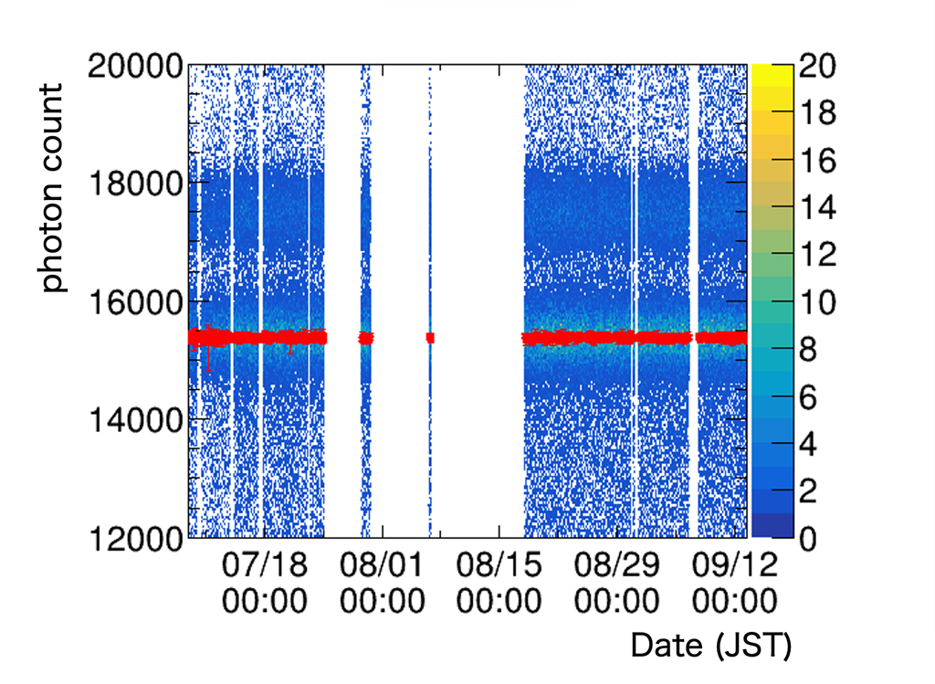
EL light intensity varies over time depending on gas temperature, pressure, and purity. Therefore, corrections are applied for every 30 minutes by using the peaks. Figure 15 shows the time variation.

5.3.2 Correction of -dependence
There is an attenuation of ionization electrons during drift due to attachment by impurities. The photon count of clusters is shown in Fig. 16 as a function of the z position, from which, the attenuation length was determined to be . This corresponds to the electron lifetime of . The photon counts are corrected for every sampling of the waveforms using this attenuation length.
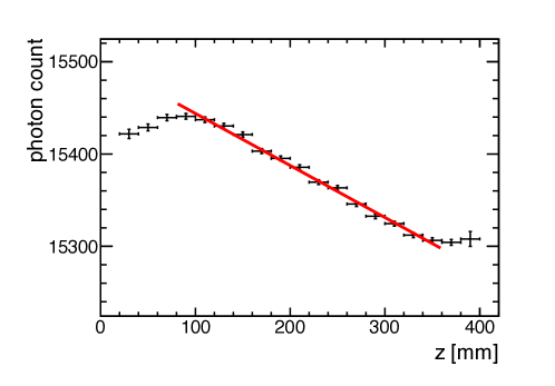
Deviations from the fit function are observed on both the larger and smaller sides of z-position, but the cause is not known. Possible reasons include mis-reconstruction of the z-position and the MPPC nonlinearity correction not being fully functional due to the analog filter or sampling effects.
5.3.3 Overall fine-tuning for the non-linearity of MPPCs
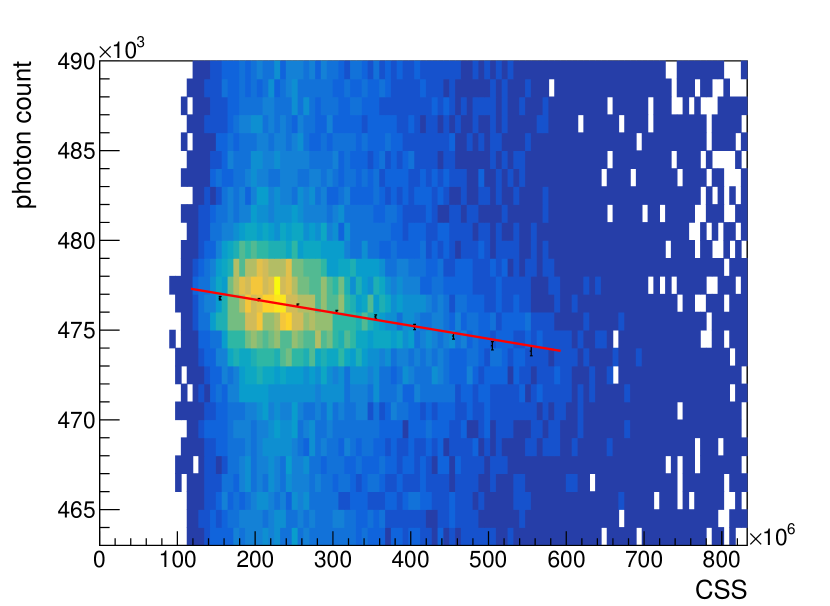
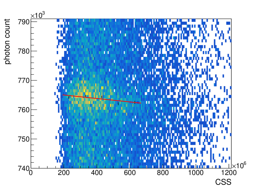
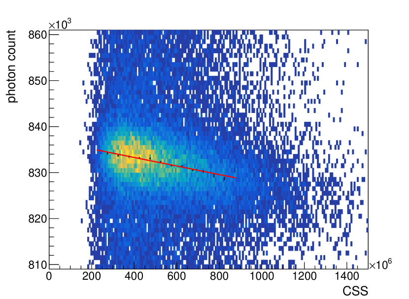
If there remains overall difference between the true and the measured MPPC non-linearity, the effect appears as a linear relation between the photon counts and corrected squared sum, CSS: of events10.1093/ptep/ptad146 . Here, is the correction factor other than the MPPC non-linearity, and are the photon counts for each sampling of the waveform after the MPPC non-linearity correction. For this measurement, we used the photopeaks of the gamma rays from , gamma rays from , and the double escape peak of gamma rays from . Distributions of the photon counts and the CSS for these peaks are shown in Fig. 17. The overall correction parameter was determined from these distributions. With this, the MPPC non-linearity is corrected again.
|
|
6 Detector performance
6.1 Energy resolution
The obtained EL photon count spectrum is shown in Fig. 18.
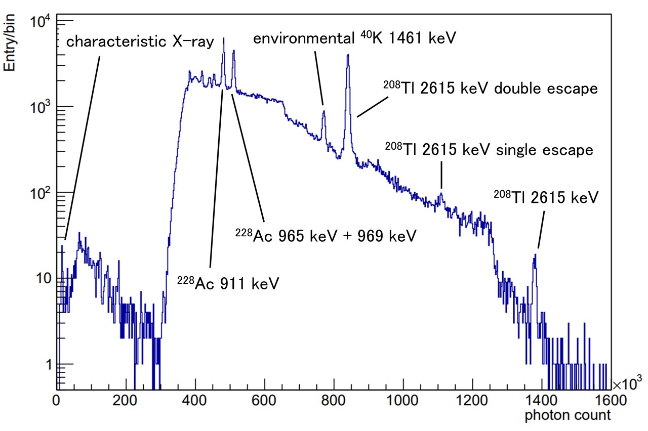
The gamma ray peak and the single escape peak are clearly seen. Each peak of the spectrum was fitted with a combination of a Gaussian and a linear functions, and the results are summarized in Table 1.
| Energy | photon counts | resolution [FWHM] | |
|---|---|---|---|
| environmental | |||
| Double escape of | |||
By interpolating these results, the energy resolution at 136Xe Q value was estimated. Two types of energy dependence are considered: a case in which statistical fluctuation dominate () and a case in which systematic errors proportional to the energy exist (). Figure 19 shows the result of the interpolation to the Q value.
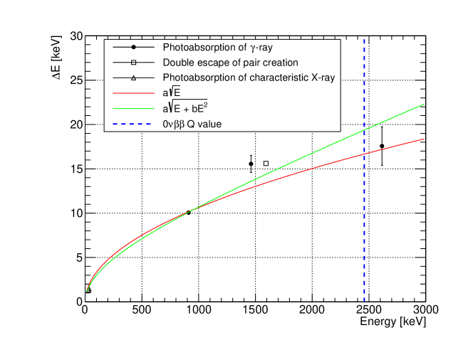
The estimated energy resolution at the Q value is for the form of and for the form of .
6.2 Track reconstruction
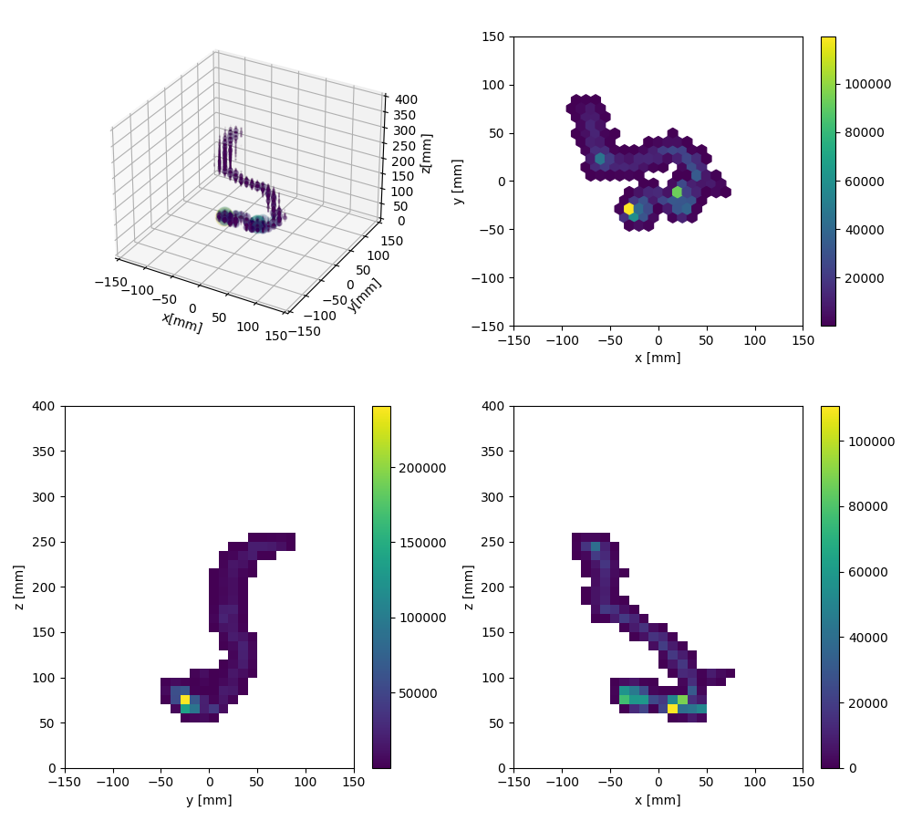
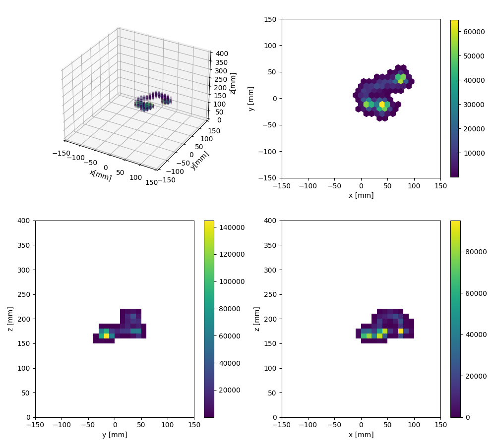
These events correspond to the photoelectric absorption peak and the double escape peak of gamma rays of 208Tl respectively. At the end of the track, there is a “blob” associated with high energy loss. In the event, there is one blob produced at the electron stop. The event produces two blobs at the end of electron and positron track, respectively. Since two blobs occur in the event as well, it is possible to distinguish the single-electron events by gamma ray backgrounds by using the track information.
7 Conclusion
We have newly developed a CW multiplier to generate high voltage and supply to the AXEL detector inside a gas chamber and installed it into a prototype detector.
By implementing it on an FPC, we reduced the size and suppressed outgassing, making it possible to install it in the narrow space of a high-pressure xenon gas chamber. Surface discharge on the circuit was suppressed by applying additional insulating coating.
We installed the CW multiplier with 40 stages in a prototype detector, applied and conducted data acquisition for 77 days, achieving an energy resolution of at and succeeded to reconstruct 3D tracks. The electrical noise from the CW multiplier superimposed on the ELCC waveform is within one ADC count, confirming that its impact on the energy resolution is sufficiently small. We have demonstrated continuous operation of the CW multiplier in the high-pressure xenon gas TPC without deteriorating the detector performance.
Acknowledgements
This work was supported by the JSPS KAKENHI Grant Numbers 18H05540, 18J00365, 18J20453, 19K14738, 20H00159, 20H05251, and the JST SPRING, Grant Number JPMJSP2114. We also appreciate the support for our project by Institute for Cosmic Ray Research, the University of Tokyo. The development of the front-end board AxFEB is supported by Open-It (Open Source Consortium of Instrumentation).
References
- (1) W. H. Furry, Phys. Rev., 56, 1184–1193 (Dec 1939).
- (2) S. Abe et al., Phys. Rev. Lett., 130, 051801 (Jan 2023).
- (3) J. D. Cockcroft, E. T. S. Walton, E. Rutherford, Proceedings of the Royal Society of London. Series A, Containing Papers of a Mathematical and Physical Character, 136(830), 619–630 (1932), https://royalsocietypublishing.org/doi/pdf/10.1098/rspa.1932.0107.
- (4) A. Marchionni et al., Journal of Physics: Conference Series, 308(1), 012006 (jul 2011).
- (5) D. R. Nygren, The optimal detectors for wimp and 0-neutrino double beta decay searches: identical high pressure xenon gas tpc, In 2007 IEEE Nuclear Science Symposium Conference Record, volume 2, pages 1051–1055 (2007).
- (6) V. Álvarez et al., Journal of Instrumentation, 8(09), P09011 (sep 2013).
- (7) P. Novella et al., Journal of High Energy Physics, 2023(9), 190 (Sep 2023).
- (8) M. Yoshida et al., Progress of Theoretical and Experimental Physics, 2024(1), 013H01 (12 2023), https://academic.oup.com/ptep/article-pdf/2024/1/013H01/55371817/ptad146.pdf.
- (9) M. M. Weiner, Review of Scientific Instruments, 40(2), 330–333 (02 1969), https://pubs.aip.org/aip/rsi/article-pdf/40/2/330/19117236/330_1_online.pdf.
- (10) S. Ban et al., Progress of Theoretical and Experimental Physics, 2020(3), 033H01 (03 2020), https://academic.oup.com/ptep/article-pdf/2020/3/033H01/32970446/ptaa030.pdf.