Exploring the energy spectrum of a four-terminal Josephson junction: Towards topological Andreev band structures
Abstract
Hybrid multiterminal Josephson junctions (JJs) are expected to harbor a novel class of Andreev bound states (ABSs), including topologically nontrivial states in four-terminal devices. In these systems, topological phases emerge when ABSs depend on at least three superconducting phase differences, resulting in a three-dimensional (3D) energy spectrum characterized by Weyl nodes at zero energy. Here, we realize a four-terminal JJ in a hybrid Al/InAs heterostructure, where ABSs form a synthetic 3D band structure. We probe the energy spectrum using tunneling spectroscopy and identify spectral features associated with the formation of a tri-Andreev molecule, a bound state whose energy depends on three superconducting phases and, therefore, is able to host topological ABSs. The experimental observations are well described by a numerical model. The calculations predict the appearance of four Weyl nodes at zero energy within a gap smaller than the experimental resolution. These topological states are theoretically predicted to remain stable within an extended region of the parameter space, well accessible by our device. These findings establish an experimental foundation to study high-dimensional synthetic band structures in multiterminal JJs, and to realize topological Andreev bands.
I Introduction
Josephson junctions (JJs) are key elements of superconducting circuits, used in quantum technology applications and fundamental research. In a superconducting-normal conductor-superconducting junction, supercurrent transport is mediated by Andreev bound states (ABSs), electron-hole superposition states confined within the normal area. The ABS energy depends on the phase difference between the superconducting wave functions of the two leads [1, 2, 3, 4]. Recently, these electronic modes have been the subject of extensive study [5, 6, 7, 8, 9, 10, 11, 12], including the coherent manipulation of ABSs [13, 14, 15, 16] and the exploration of topological superconductivity [17, 18, 19, 20].
In multiterminal JJs (MTJJs), where three or more superconducting terminals are linked to a single normal scattering region, ABSs form synthetic band structures which are expected to host a wide range of properties not attainable in two-terminal devices. Among the most intriguing prospects is the potential to realize topologically nontrivial phases in the three-dimensional (3D) band structure of four-terminal JJs (4TJJs), with Weyl nodes arising in the energy spectrum [21, 22, 23, 24, 25, 26, 27]. Topological phases in these systems are inherently robust with respect to external perturbations [21], making them particularly appealing for applications in quantum information processing [28, 29] and spintronics [30].
A first set of studies on MTJJs focused on their transport properties, including the signatures of Cooper pair quartets [31, 32, 33, 34, 35] and the flow of supercurrents across multiple superconducting leads [36, 37, 38, 39, 40, 41, 42]. Recently, MTJJs have been proposed as a platform to realize Andreev molecules—a system where ABSs hybridize due to the spatial overlap of their wave functions [43, 44, 45, 46, 47], resulting in delocalized states that extend across all leads and exhibit nonlocal Josephson effect [43, 48, 49, 50, 51]. In Andreev molecules, two primary coherent transport processes occur: double elastic cotunneling and double crossed Andreev reflection [52, 31, 43], both essential for the generation of Cooper pair multiplets [31, 32, 53] and for engineering Kitaev chains [54] in quantum dot arrays [55, 56, 57, 58, 59, 60, 61, 62, 63, 64, 65]. Detailed understanding of Andreev band structures in multiterminal devices can be gained through local spectroscopy, which has been employed to probe hybridized ABSs [66, 67], as well as spin-split energy levels and ground state parity transitions [68, 69]. In these experiments, phase biasing allowed the exploration of ABS spectra as a function of up to two superconducting phase differences [70, 66, 69]. However, realizing topological phases with nontrivial Chern numbers strictly requires independent tuning of three phase degrees of freedom [21, 71, 72, 24], a challenge that remains to be addressed.

In this work, we realize a 4TJJ where three phases are independently controlled through flux biasing. We probe the ABS energy spectrum of the system across the entire 3D phase space using tunneling spectroscopy. Moreover, we observe the simultaneous hybridization of three ABSs, i.e., the formation of a so called tri-Andreev molecule, when the three phases are tuned close to . Our findings are supported by a theoretical model, which qualitatively reproduces the main features of the measured Andreev spectra. Furthermore, our simulations indicate that the Andreev bands undergo a phase-controlled topological transition in which hybridization induces a band inversion accompanied by the appearance of Weyl nodes. Due to the finite resolution of the tunneling spectroscopy, with a linewidth of eV, the gapless states (Weyl nodes) cannot be experimentally distinguished from the gapped states. Finally, we study the robustness of the topological phase under variations of experimentally addressable parameters, finding that the regime best describing our device is well within the topological region. Overall, our work provides access to Andreev band structures in three synthetic dimensions, creating an experimental platform and practical guidelines for the realization of topological states in hybrid multiterminal devices.
II Experimental setup and 3D phase control
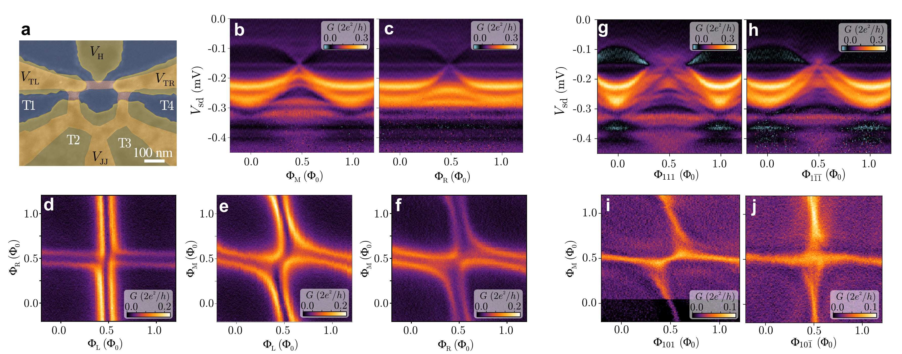
The device under study, shown in Fig. 1(a), consists of a 4TJJ embedded in a triple-loop geometry. It is realized in an InAs/Al heterostructure [73, 74] where the epitaxial Al layer is selectively removed to expose the III–V semiconductor below. Three flux-bias lines are patterned on top of a uniform dielectric layer to generate the external magnetic fluxes threading the three interconnected superconducting loops (L, M, R). This enables us to control the phase differences between the four terminals (T1-T4). The latter couple with a common semiconducting region [see Fig. 1(b)] where a superconducting island with diameter nm is left at its center to partially screen the probe gate voltages. By design, the minimum distance between neighboring terminals is 50 nm, while the distance between T1 and T4 is 220 nm. All these lengths are small in comparison with the superconducting coherence length in the InAs 2DEG, estimated to be [49]. Four gate electrodes on the dielectric layer are energized by voltages ( {TL, TR, H, JJ}), allowing for electrostatic tuning of the electron density in the InAs layer below. Tunneling spectroscopy of the scattering area is performed by measuring the differential conductance across a tunneling barrier, formed by depleting the InAs region below the gates and (see Supplemental Material [75], Sec. I for additional details). The device was measured in a dilution refrigerator with a base temperature of about using lock-in techniques, with a DC voltage bias and an AC voltage bias of amplitude applied between the probe and the four terminals. More information about materials, fabrication and measurement setup is available in Ref. [66].

Figure 1(c) shows a typical tunneling spectrum measured by varying the flux-line current and the DC bias . The flux-dependent ABS spectrum is visible outside a transport gap of , that is due to the superconducting probe ( is the superconducting gap). Two flux-independent conductance peaks at highlight the probe gap edges and are attributed to multiple Andreev reflection processes. Assuming a BCS-like density of states (DOS) for the superconducting probe with peaks at energy , is expected to have a resonance at a voltage when a peak is present in the DOS of the scattering area at energy . Consequently, spectroscopic features observed at correspond to DOS peaks at zero energy () in the scattering area. When half of a superconducting flux quantum () induced by the left flux line penetrates loop L, the superconducting phase difference is tuned to and the ABS energy approaches zero energy as for a highly transparent two-terminal JJ [2]. Notably, the dispersion shows an additional modulation with a larger periodicity in , which is evident in the map shown in Fig. 1(d) measured at constant by varying and . Here, we observe a slower modulation along the diagonal direction , caused by the magnetic flux generated by lines L and R impinging through the middle loop. A useful way to navigate within the 3D flux space is to consider the cubic unit cell defined by the three independent magnetic fluxes , , , as schematically illustrated in the insets of Fig. 1(d,e). Within this framework, the - map follows a tilted plane sketched in gray, whose orientation is defined by the mutual inductance matrix :
| (1) |
where is an offset defining the corner of a unit cell. In order to cut the unit cell in a controlled way, we compensate for the cross-coupling between loops and flux lines by simultaneously setting the three currents , and needed to reach a flux point , according to Eq. (1). Figure 1(e) shows the differential conductance map measured in this way by sweeping the fluxes and and keeping . As a result, a periodic square net is obtained, demonstrating independent flux control over the three loops. More details about the current-to-flux remapping and how to extract the mutual inductance matrix elements are provided in Ref. [75], Sec. II.

III ABS energy dispersion in the 3D flux space
Having established a measurement protocol that allows for independent flux control, we systematically map the ABS energy spectrum in the 3D flux space. Owing to the periodicity of the spectrum, we can restrict our investigation to a single 3D flux unit cell. We start with a simple case where we sweep the flux threading a loop while keeping the other two fluxes at zero, as shown in Fig. 2(a) for varying . The energy spectrum reveals the dispersion of a highly transparent ABS, that we identify as the mode formed between the terminal pair T1-T2. The large but finite transparency is expected to prevent the band from reaching zero energy, forming a minigap between the electron- and hole-like branches of the ABS spectrum [3]. However, this small energy gap is not experimentally revolved due to the sizable spectral broadening, estimated to be eV (see Ref. [75], Sec. III). Notably, the ABS dispersion does not reach the superconducting gap edge, but it is reduced to , potentially due to the repulsion with the lower-transmission states visible at mV. Figure 2(b) shows the dispersion of the ABSs formed between T2-T3, which are tuned by sweeping . Similar to the previous case, the spectrum is dominated by a brighter highly transparent mode having the same reduced dispersion, and a low-transmission manifold of states at lower energies. The dispersion of the modes formed between T3 and T4 (shown in Ref. [75], Sec. III) is qualitatively equivalent to the one along . In the following, we focus on the three high-transmission ABSs that we label , and as shown in Fig. 1(b).
To have an overview on how such states disperse in the flux space, we map the differential conductance fixed at within the whole 3D unit cell. In Fig. 2(c) we plot for values larger than , i.e., where the DOS is nonzero. At this value, the Andreev dispersions are cut twice around , forming pairs of parallel conductance lines along the cube faces. At the center of each face, the ABSs do not cross each other, but they rather interact opening avoided crossings, as highlighted in the face maps of Fig. 2(d,e). These avoided crossings are spectral signatures characteristic of bi-Andreev molecular states formed by the hybridization of two ABSs, which have recently been observed in three-terminal devices [66]. Notably, the four-terminal device presented here acts as an effective three-terminal system on the cube faces, i.e., when one flux is kept fixed to zero.
To better define directions in the 3D flux space, we introduce a crystallographic-like notation, where the three flux axes (, and ) are denoted as , , and , respectively. The hybridization lifts the degeneracy of the original two-terminal ABSs, splitting the dispersion in two bands as observed in the spectra in Figs. 2(f) and 2(g), measured along the directions (110) and (101) (white arrows in Figs. 2(d) and 2(e), respectively). A larger splitting is observed along the (110) direction (f) compared to (101) cut (g), indicating a stronger coupling between the nearest neighbor ABSs L and M. A weaker hybridization is instead expected between L and R, due to their smaller wavefunction overlap. In Fig. S4 [75], additional tunneling spectra show that the energy splitting is much smaller along the perpendicular directions and , as expected when the interacting ABSs have opposite phases [43, 47, 66]. Thus, our observations reveal a significant hybridization between all three ABSs, which couple in pairs to form bi-Andreev molecules on each face of the cubic unit cell.

IV Exploring the center of the unit cell
The device configurations discussed so far reproduce the behavior of either two-terminal devices (when two phase differences are kept to zero, i.e., along the unit cell edges) or three-terminal ones (along the unit cell faces, where only one phase difference is kept to zero). Inside the unit cell, all the phase differences are nonzero, leading to a more complex ABS spectrum achievable only with four or more leads. To explore such configurations, we slice the cubic cell from the - face to the center along parallel planes measured at different values and at , as shown in Fig. 3(a). At this value, we probe the energy spectrum near the maxima of the ABSs, resulting in one conductance line per state. By increasing , the conductance becomes asymmetric around the center of the plot and develops a maximum at . More detailed discussions of this figure are presented in Ref. [75], Sec. V. Moving further to , the map recovers its inversion symmetry, featuring two lobes of low conductance around the center. In this configuration, one would expect to measure constant conductance across the entire plane, since is fixed at its energy maximum. Instead, the energy cut along [Fig. 3(b)] reveals that the state has a relatively weak dispersion just below mV.
We explain the weak influence of on this ABSs in terms of mutual inductive coupling between loops. When and are swept in-phase (), two opposite currents flow along the two long sides of loop M, as shown in Fig. 3(c). These currents induce two parallel flux contributions to , providing an additional phase difference between T2 and T3. When and are swept with opposite sign, i.e., along , the two currents flow in the same direction as sketched in Fig. 3(e), and the two induced fluxes cancel each other out. Indeed, the spectrum measured along this direction [Fig. 3(d)] shows that forms a flat band independent of the other two fluxes just below mV.
In Fig. 3(d), we also observe two dispersive bands representing the hybridized states and having their maxima at . Here, they interact with the -derived flat band which significantly decreases its energy to mV. This indicates that an additional gap between the electron- and hole-like branches of the overall ABS spectrum is opened in addition to the minigap formed by the finite junction transparency. In the following, we show that this spectral feature marks the hybridization among three two-terminal ABSs occurring when they are tuned to the same energy, i.e., the formation of a tri-Andreev molecule.

V Theoretical model
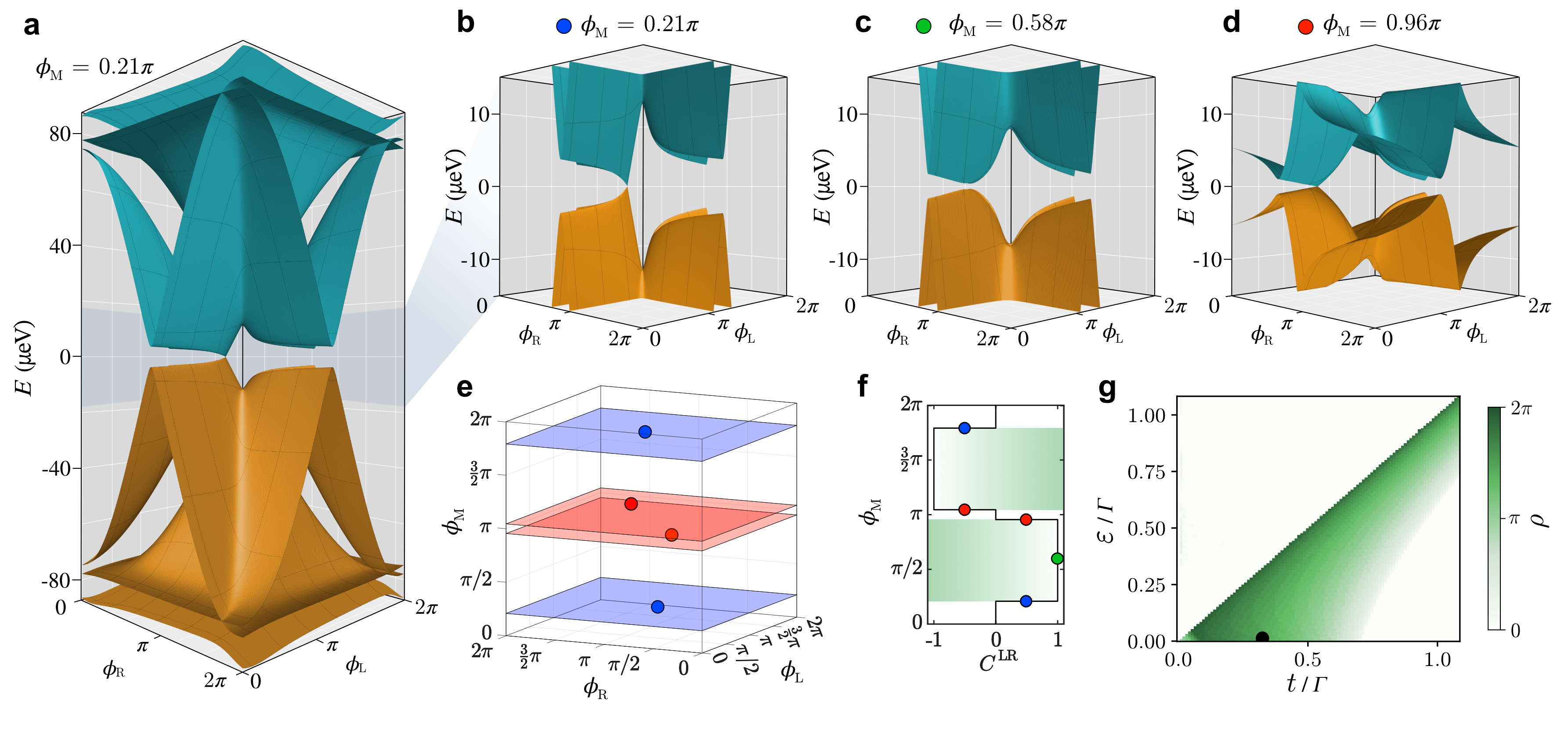
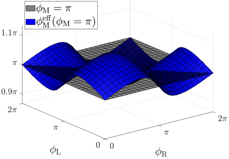
To better understand how the hybridization between ABSs reshapes the complex Andreev band structure observed in the previous paragraph, we develop a theoretical model schematically represented in Fig. 4(a). The model features four superconducting leads coupled to a normal scattering region described by means of three coupled quantum dots. The superconducting phase differences (or equivalently magnetic fluxes ) are defined between the leads using the same convention introduced in Fig. 1(a). Each dot contains two noninteracting spin-degenerate levels of energy (), and is coupled to the neighboring leads with a coupling strength characterized by the parameter , as well as to the other dots, described by the parameter . All dot-lead couplings and interdot couplings are assumed to be equal. We note that the choice of a quantum dot network provides a convenient description of a normal region hosting discrete ABSs, with the degree of hybridization among them determined by . No Coulomb interaction or charging energy are introduced in the system, as the dots are strongly coupled to the leads. To compare with the experimental data, we compute the total DOS projected onto the three dots as a function of the energy and the three superconducting phase differences (fluxes ), indicated in Fig. 4(a). Furthermore, to include the effect of the mutual inductive coupling between the superconducting loops, which causes a nonlinear cross-dependence between the phases (magnetic fluxes), we remap them to effective phases (effective magnetic fluxes ) using the relations:
where for . Here, , is the strength of the mutual coupling and introduces nonsinusoidal character to . Additional details on the model are discussed in Ref. [75], Secs. VI and VII. Figure 4(b) illustrates the influence of on as a consequence of the mutual coupling, highlighting a nonlinear behavior when are varied together with .
The simulated DOS as a function of energy and of while is shown in Fig. 4(c). The two energy levels in each of the three dots give rise to two distinct manifolds comprising three modes each. As expected, only one state per manifold has a significant energy dispersion, while the others remain mostly constant in energy. Similar to the tunneling spectra in Fig. 2(a,b), the simulated band structure exhibits one resonance that approaches at , forming a cusp consistent with an isolated high-transmission ABS. Figure 4(d) displays the simulated - plane for constant flux and constant energy , which corresponds to the measurement shown in Fig. 3(a). The presence of two lobes of minimum DOS around is captured by the model as a result of the mutual coupling between the phases.
To focus on the effects of ABS hybridization, we consider the direction (in which mutual inductance effects are negligible) and simulate the Andreev spectra as a function of for different values of [Fig. 4(f)]. At , M remains flat at high energy, while both R and L form dispersing bands which are nearly degenerate in energy. By increasing , the flat state approaches zero energy and forms avoided crossings with the dispersing states. These three nondegenerate ABSs resemble the energy levels of a tri-atomic molecule, where three molecular orbitals (bonding, nonbonding and antibonding) are split in energy, as conceptually depicted in Fig. 4(e). At , the state M reaches the energy closest to zero and remains constant around that energy. Here, its dispersion bends downwards from zero energy as observed in the corresponding measurement in Fig. 3(c). These results support the interpretation that our device hosts three ABSs hybridizing among each other, forming a tri-Andreev molecule delocalized over the four superconducting terminals.
VI tri-Andreev molecule
Supported by our theoretical model, we investigate more complex spectral features measured along the diagonals of the cubic unit cell, when all three fluxes are varied. Figure 5(a) shows a map measured at along the - plane sketched in the schematic on the left. As previously discussed in Sec. III, L and R are already hybridized along the direction, as also visible by the splitting of the conductance line at and . When is tuned to , these hybridized states mix with M forming an avoided crossing which is well reproduced by the simulation displayed in Fig. 5(b). Taking an energy cut along the direction [gray arrow in (a)], we observe how the energy spectrum is affected by the hybridization, as shown in Fig. 5(c). Here, the bands split in energy forming an M-shape dispersion close to zero energy. Notably, such effect is much stronger compared to the one observed for the bi-Andreev molecules in Fig. 2(f,g). By simulating the same energy spectrum [Fig. 5(d)], we reproduce a similar M-shape of the topmost band and reveal the energy splitting between the three bands representing the bonding, nonbonding and antibonding molecular states illustrated in Fig. 4(e).
As discussed in Sec. III for the bi-Andreev molecules, the energy splitting induced by the hybridization is strongly anisotropic in the phase space. Figure 5(e) shows the conductance map along the - plane sketched in the schematic on the left. Here, the dispersions of L and R overlap with each other at , but split when is swept towards . Notably, the splitting appears larger along the direction compared to , since L has a slightly larger transparency than R (see [75], Sec. IV). Also, the horizontal conductance resonance representing the maximum of M significantly decreases in intensity approaching the center of the map. The simulation in Fig. 5(f) reproduces the opening of a low conductance region at the crossing point, which ultimately derives from the splitting at observed in the simulated energy spectra in Fig. 4(f). Indeed, those dispersions represent horizontal energy-dependent cuts of Fig. 5(f), at values indicated by the colored arrows. Taking an energy-dependent cut along the direction [Fig. 5(g)], we observe a sizable splitting into two bands, but smaller than the splitting observed along the direction. The overall hybridization strength is indeed reduced along the direction since two phases always have opposite values. Therefore, two bands are expected to remain nearly degenerate, as reproduced in the simulated spectrum in Fig. 5(h).
In summary, the dispersion of a tri-Andreev molecule is characterized by an anisotropic energy splitting, larger along the direction and weaker along its perpendicular direction . This is directly reflected into the different shapes of the avoided crossings observed at the center of the cube diagonal conductance maps of Fig. 5(a,e). The spectral signatures of a tri-Andreev molecule discussed here are also observed in a second device (see [75], Sec. VIII).
VII Topological Andreev bands
The hybridization between the three ABSs in our device leads to the formation of molecular-like states whose energy depends on all three superconducting phase differences. This property is one of the requirements for the formation of Weyl nodes, which would appear as zero-energy crossing points with linear dispersion as a function of all the three phases. In the following, we analyze the simulated Andreev band structure matching our experimental results. In Fig. 6(a), we show the ABSs spectrum extracted from the maxima of the density of states for . Here, the two particle-hole symmetric bands closest to the Fermi level form a zero energy crossing at as highlighted in the zoomed-in plot in Fig. 6(b). Increasing , we obtain gapped states [see Fig. 6(c)] with a small energy gap. The gap is closed again at , where another zero-energy crossing appears at [Fig. 6(d)]. Within the whole cubic unit cell we find four zero-energy crossings appearing in two pairs (red and blue points in Fig. 6(e)), which are related by time-reversal symmetry.
As shown in Ref. [76, 77, 78], the full information about the topology of the ABS spectrum is encoded in the topological Hamiltonian, , given by the inverse of the central Green’s functions evaluated at zero energy, i.e., . depends on the dimensionless parameters and [24, 27] (see more details in Ref. [75], Sec. VII). The values of and used for the DOS simulations matching our measurements correspond to and . By diagonalizing , we obtain the eigenvectors and the corresponding spin-degenerate eigenenergies. To establish the topological properties of the ABSs, we compute the topological invariant following the numerical method in Ref. [79]. The Chern number is given by
| (2) |
with the total Chern number as the sum over all occupied bands and represents the Berry curvature calculated at fixed . Figure 6(f) shows two distinct nontrivial topological phases having Chern number equal to within extensive intervals indicated by the green areas. Therefore, the zero energy crossing points in (e) are positively (blue) and negatively (red) charged Weyl nodes appearing in the energy spectra (b,d) as the states cross the Fermi level. The eigenenergies of the topological Hamiltonian for the same parameters as in Fig. 6 are shown in Fig. S7 [75]. The eigenenergies exhibit zero-energy states exactly when one local maximum of the DOS is at zero energy, as expected. Notably, the spectrum shown in Fig. 6(c) represents a topological insulating phase with a small energy gap. Since such features are masked by the relatively large spectral broadening in our measurements, we cannot experimentally confirm the predicted topological phase transitions.
To evaluate the robustness of the topological regime in our simulations, we calculate the extension of the region in where the Chern number differs from zero [green areas in (f)] as a function of the two key parameters of our model, and . The phase diagram in Fig. 6(g) shows a first topological transition when the hybridization exceeds . Intuitively, the hybridization has to be large enough to push one state through zero energy, a mechanism analogous to the band inversion driven by spin-orbit coupling occurring in topological insulators [80]. By further increasing , the two opposite charged Weyl nodes get closer to each other gradually reducing to zero. At this point, the oppositely charged Weyl nodes annihilate with each other completely suppressing the topological phase. The parameters used for simulating our measurements corresponds to and , which places our system well within the calculated topological region as indicated by the black dot in Fig. 6(g).
VIII Discussion and conclusions
In this work, we studied the hybridization between ABSs in a 4TJJ and demonstrated the formation of a tri-Andreev molecule. This state, whose energy is controlled by three superconducting phase differences, is expected to support topological Andreev bands. According to our model, Weyl nodes emerge when the hybridization shifts at least one ABS through zero energy, inducing an inversion between electron- and hole-like bands in certain regions of the phase space. By varying , the system undergoes four topological transitions marked by Weyl nodes as shown in Fig.6(f). The Andreev bands as a function of - have an energy gap ranging between 0 (at the Weyl nodes) and , depending on . The resolution of tunneling spectroscopy, approximately , prevents us from experimentally resolving any gapped states in the low-energy spectrum. Thus, the spectral detection of Weyl nodes would be facilitated by a larger minigap, which could be obtained through an increase of the superconducting gap or by a enhanced device tunability. For example, a larger minigap would be obtained by making the coupling parameters [see in Fig. 4(a)] asymmetric or by increasing , while keeping a sufficiently large hybridization strength. The phase diagram shown in Fig. 6(g) provides a useful guideline for engineering these parameters while preserving the topological properties of the device.
The large transparency and hybridization strength observed in our 4TJJ already fall well into the stability range of the topological state. Experimental techniques with higher energy resolution would be highly favorable for confirming the presence of Weyl nodes in the ABS spectrum, even in systems with such a large transparency. Microwave spectroscopy, in particular, offers sub- resolution, making it well suited for this purpose. Furthermore, hybrid InAs/Al heterostructures are readily integrated in circuit QED architectures [81, 82, 14, 83, 11, 84], offering a tangible prospect for studies of topological Andreev band structure. The employment of polarized microwave radiation can also make this technique sensitive to the Berry curvature [24].
In summary, we realized a phase-controlled 4TJJ and studied its energy spectrum using tunneling spectroscopy. The measurement protocol based on independent flux control developed here allows the systematic exploration of the Andreev spectrum in the 3D phase space. We identified the spectral signatures of a tri-Andreev molecule resulting from the simultaneous hybridization of three ABSs. A numerical model reproduced the key experimental observation, and suggested that the current generation of devices already hosts topological Andreev bands. In the light of our results, phase-tunable MTJJs offer new opportunities for studying topological phases in high-dimensional synthetic band structures and developing novel superconducting quantum circuits [85].
IX Data availability
The data that support the findings of this article will be available on Zenodo.
X Acknowledgments
We thank Manuel Hinderling for useful discussions. We thank the Cleanroom Operations Team of the Binnig and Rohrer Nanotechnology Center (BRNC) for their help and support. D.C.O., A.E.S. and W.B. acknowledge support by the Deutsche Forschungsgemeinschaft (DFG; German Research Foundation) via SFB 1432 (Project No. 425217212) and Project No. 467596333, and by the Excellence Strategy of the University of Konstanz via a Blue Sky project. J.C.C. thanks the Spanish Ministry of Science and Innovation (Grant PID2020-114880GB-I00) for financial support and the DFG and SFB 1432 for sponsoring his stay at the University of Konstanz as a Mercator Fellow. W.W. acknowledges support from the Swiss National Science Foundation (grant number 200020_207538). F.N. acknowledges support from the European Research Council (grant number 804273) and the Swiss National Science Foundation (grant number 200021_201082).
XI References
References
- Andreev [1964] A. F. Andreev, Thermal conductivity of the intermediate state of superconductors, Sov. Phys. JETP 19, 1228 (1964).
- Beenakker and van Houten [1991] C. W. J. Beenakker and H. van Houten, Josephson current through a superconducting quantum point contact shorter than the coherence length, Phys. Rev. Lett. 66, 3056 (1991).
- Beenakker [1991] C. W. J. Beenakker, Universal limit of critical-current fluctuations in mesoscopic Josephson junctions, Phys. Rev. Lett. 67, 3836 (1991).
- Furusaki and Tsukada [1991] A. Furusaki and M. Tsukada, Current-carrying states in Josephson junctions, Phys. Rev. B 43, 10164 (1991).
- Pillet et al. [2010] J.-D. Pillet, C. H. L. Quay, P. Morfin, C. Bena, A. L. Yeyati, and P. Joyez, Andreev bound states in supercurrent-carrying carbon nanotubes revealed, Nat. Phys. 6, 965 (2010).
- Bretheau et al. [2013a] L. Bretheau, Ç. Ö. Girit, H. Pothier, D. Esteve, and C. Urbina, Exciting Andreev pairs in a superconducting atomic contact, Nature 499, 312 (2013a).
- Bretheau et al. [2013b] L. Bretheau, Ç. Ö. Girit, C. Urbina, D. Esteve, and H. Pothier, Supercurrent spectroscopy of Andreev states, Phys. Rev. X 3, 041034 (2013b).
- Lee et al. [2014] E. J. H. Lee, X. Jiang, M. Houzet, R. Aguado, C. M. Lieber, and S. D. Franceschi, Spin-resolved Andreev levels and parity crossings in hybrid superconductor–semiconductor nanostructures, Nat. Nanotechnol. 9, 79 (2014).
- van Woerkom et al. [2017] D. J. van Woerkom, A. Proutski, B. van Heck, D. Bouman, J. I. Väyrynen, L. I. Glazman, P. Krogstrup, J. Nygård, L. P. Kouwenhoven, and A. Geresdi, Microwave spectroscopy of spinful Andreev bound states in ballistic semiconductor Josephson junctions, Nat. Phys. 13, 876 (2017).
- Hays et al. [2020] M. Hays, V. Fatemi, K. Serniak, D. Bouman, S. Diamond, G. de Lange, P. Krogstrup, J. Nygård, A. Geresdi, and M. H. Devoret, Continuous monitoring of a trapped superconducting spin, Nat. Phys. 16, 1103 (2020).
- Tosi et al. [2019] L. Tosi, C. Metzger, M. F. Goffman, C. Urbina, H. Pothier, S. Park, A. L. Yeyati, J. Nygård, and P. Krogstrup, Spin-orbit splitting of Andreev states revealed by microwave spectroscopy, Phys. Rev. X 9, 011010 (2019).
- Nichele et al. [2020] F. Nichele, E. Portolés, A. Fornieri, A. M. Whiticar, A. C. C. Drachmann, S. Gronin, T. Wang, G. C. Gardner, C. Thomas, A. T. Hatke, M. J. Manfra, and C. M. Marcus, Relating Andreev bound states and supercurrents in hybrid Josephson junctions, Phys. Rev. Lett. 124, 226801 (2020).
- Janvier et al. [2015] C. Janvier, L. Tosi, L. Bretheau, C. O. Girit, M. Stern, P. Bertet, P. Joyez, D. Vion, D. Esteve, M. F. Goffman, H. Pothier, and C. Urbina, Coherent manipulation of Andreev states in superconducting atomic contacts, Science 349, 1199 (2015).
- Hays et al. [2018] M. Hays, G. de Lange, K. Serniak, D. J. van Woerkom, D. Bouman, P. Krogstrup, J. Nygård, A. Geresdi, and M. H. Devoret, Direct microwave measurement of Andreev-bound-state dynamics in a semiconductor-nanowire Josephson junction, Phys. Rev. Lett. 121, 047001 (2018).
- Hays et al. [2021] M. Hays, V. Fatemi, D. Bouman, J. Cerrillo, S. Diamond, K. Serniak, T. Connolly, P. Krogstrup, J. Nygård, A. L. Yeyati, A. Geresdi, and M. H. Devoret, Coherent manipulation of an Andreev spin qubit, Science 373, 430 (2021).
- Pita-Vidal et al. [2023] M. Pita-Vidal, A. Bargerbos, R. Žitko, L. J. Splitthoff, L. Grünhaupt, J. J. Wesdorp, Y. Liu, L. P. Kouwenhoven, R. Aguado, B. van Heck, A. Kou, and C. K. Andersen, Direct manipulation of a superconducting spin qubit strongly coupled to a transmon qubit, Nat. Phys. 19, 1110 (2023).
- Mourik et al. [2012] V. Mourik, K. Zuo, S. M. Frolov, S. R. Plissard, E. P. A. M. Bakkers, and L. P. Kouwenhoven, Signatures of Majorana fermions in hybrid superconductor-semiconductor nanowire devices, Science 336, 1003–1007 (2012).
- Nichele et al. [2017] F. Nichele, A. C. C. Drachmann, A. M. Whiticar, E. C. T. O’Farrell, H. J. Suominen, A. Fornieri, T. Wang, G. C. Gardner, C. Thomas, A. T. Hatke, P. Krogstrup, M. J. Manfra, K. Flensberg, and C. M. Marcus, Scaling of Majorana zero-bias conductance peaks, Phys. Rev. Lett. 119, 136803 (2017).
- Fornieri et al. [2019] A. Fornieri, A. M. Whiticar, F. Setiawan, E. Portolés, A. C. C. Drachmann, A. Keselman, S. Gronin, C. Thomas, T. Wang, R. Kallaher, G. C. Gardner, E. Berg, M. J. Manfra, A. Stern, C. M. Marcus, and F. Nichele, Evidence of topological superconductivity in planar Josephson junctions, Nature 569, 89 (2019).
- Ren et al. [2019] H. Ren, F. Pientka, S. Hart, A. T. Pierce, M. Kosowsky, L. Lunczer, R. Schlereth, B. Scharf, E. M. Hankiewicz, L. W. Molenkamp, B. I. Halperin, and A. Yacoby, Topological superconductivity in a phase-controlled Josephson junction, Nature , 3 (2019).
- Riwar et al. [2016] R.-P. Riwar, M. Houzet, J. S. Meyer, and Y. V. Nazarov, Multi-terminal Josephson junctions as topological matter, Nat. Commun. 7, 11167 (2016).
- Eriksson et al. [2017] E. Eriksson, R.-P. Riwar, M. Houzet, J. S. Meyer, and Y. V. Nazarov, Topological transconductance quantization in a four-terminal Josephson junction, Phys. Rev. B 95, 075417 (2017).
- Xie et al. [2018] H.-Y. Xie, M. G. Vavilov, and A. Levchenko, Weyl nodes in Andreev spectra of multiterminal Josephson junctions: Chern numbers, conductances, and supercurrents, Phys. Rev. B 97, 035443 (2018).
- Klees et al. [2020] R. L. Klees, G. Rastelli, J. C. Cuevas, and W. Belzig, Microwave spectroscopy reveals the quantum geometric tensor of topological Josephson matter, Phys. Rev. Lett. 124, 197002 (2020).
- Xie et al. [2022] H.-Y. Xie, J. Hasan, and A. Levchenko, Non-Abelian monopoles in the multiterminal Josephson effect, Phys. Rev. B 105, L241404 (2022).
- Repin and Nazarov [2022] E. V. Repin and Y. V. Nazarov, Weyl points in multiterminal hybrid superconductor-semiconductor nanowire devices, Phys. Rev. B 105, L041405 (2022).
- Teshler et al. [2023] L. Teshler, H. Weisbrich, J. Sturm, R. L. Klees, G. Rastelli, and W. Belzig, Ground state topology of a four-terminal superconducting double quantum dot, SciPost Phys. 15, 214 (2023), arXiv:2304.11982 [cond-mat] .
- Chen and Nazarov [2021a] Y. Chen and Y. V. Nazarov, Spin Weyl quantum unit: A theoretical proposal, Phys. Rev. B 103, 045410 (2021a).
- Boogers et al. [2022] V. Boogers, J. Erdmanis, and Y. Nazarov, Holonomic quantum manipulation in the Weyl disk, Phys. Rev. B 105, 235437 (2022).
- Chen and Nazarov [2021b] Y. Chen and Y. V. Nazarov, Spintronics with a Weyl point in superconducting nanostructures, Phys. Rev. B 103, 165424 (2021b).
- Freyn et al. [2011] A. Freyn, B. Douçot, D. Feinberg, and R. Mélin, Production of nonlocal quartets and phase-sensitive entanglement in a superconducting beam splitter, Phys. Rev. Lett. 106, 257005 (2011).
- Jonckheere et al. [2013] T. Jonckheere, J. Rech, T. Martin, B. Douçot, D. Feinberg, and R. Mélin, Multipair dc Josephson resonances in a biased all-superconducting bijunction, Phys. Rev. B 87, 214501 (2013).
- Pfeffer et al. [2014] A. H. Pfeffer, J. E. Duvauchelle, H. Courtois, R. Mélin, D. Feinberg, and F. Lefloch, Subgap structure in the conductance of a three-terminal Josephson junction, Phys. Rev. B 90, 075401 (2014).
- Cohen et al. [2018] Y. Cohen, Y. Ronen, J.-H. Kang, M. Heiblum, D. Feinberg, R. Mélin, and H. Shtrikman, Nonlocal supercurrent of quartets in a three-terminal Josephson junction, Proc. Natl. Acad. Sci. U.S.A. 115, 6991 (2018).
- Huang et al. [2022] K.-F. Huang, Y. Ronen, R. Mélin, D. Feinberg, K. Watanabe, T. Taniguchi, and P. Kim, Evidence for 4e charge of Cooper quartets in a biased multi-terminal graphene-based Josephson junction, Nat. Commun. 13, 3032 (2022).
- Draelos et al. [2019] A. W. Draelos, M.-T. Wei, A. Seredinski, H. Li, Y. Mehta, K. Watanabe, T. Taniguchi, I. V. Borzenets, F. Amet, and G. Finkelstein, Supercurrent flow in multiterminal graphene Josephson junctions, Nano Lett. 19, 1039 (2019).
- Graziano et al. [2020] G. V. Graziano, J. S. Lee, M. Pendharkar, C. J. Palmstrøm, and V. S. Pribiag, Transport studies in a gate-tunable three-terminal Josephson junction, Phys. Rev. B 101, 054510 (2020).
- Pankratova et al. [2020] N. Pankratova, H. Lee, R. Kuzmin, K. Wickramasinghe, W. Mayer, J. Yuan, M. G. Vavilov, J. Shabani, and V. E. Manucharyan, Multiterminal Josephson effect, Phys. Rev. X 10, 031051 (2020).
- Arnault et al. [2021] E. G. Arnault, T. F. Q. Larson, A. Seredinski, L. Zhao, S. Idris, A. McConnell, K. Watanabe, T. Taniguchi, I. Borzenets, F. Amet, and G. Finkelstein, Multiterminal inverse AC Josephson effect, Nano Lett. 21, 9668 (2021).
- Graziano et al. [2022] G. V. Graziano, M. Gupta, M. Pendharkar, J. T. Dong, C. P. Dempsey, C. Palmstrøm, and V. S. Pribiag, Selective control of conductance modes in multi-terminal Josephson junctions, Nat. Commun. 13, 5933 (2022).
- Gupta et al. [2023] M. Gupta, G. V. Graziano, M. Pendharkar, J. T. Dong, C. P. Dempsey, C. Palmstrøm, and V. S. Pribiag, Gate-tunable superconducting diode effect in a three-terminal Josephson device, Nat. Commun. 14, 3078 (2023).
- Coraiola et al. [2024a] M. Coraiola, A. E. Svetogorov, D. Z. Haxell, D. Sabonis, M. Hinderling, S. C. ten Kate, E. Cheah, F. Krizek, R. Schott, W. Wegscheider, J. C. Cuevas, W. Belzig, and F. Nichele, Flux-tunable Josephson diode effect in a hybrid four-terminal Josephson junction, ACS Nano 18, 9221–9231 (2024a).
- Pillet et al. [2019] J.-D. Pillet, V. Benzoni, J. Griesmar, J.-L. Smirr, and Ç. O. Girit, Nonlocal Josephson effect in Andreev molecules, Nano Lett. 19, 7138 (2019).
- Kornich et al. [2019] V. Kornich, H. S. Barakov, and Y. V. Nazarov, Fine energy splitting of overlapping Andreev bound states in multiterminal superconducting nanostructures, Phys. Rev. Res. 1, 033004 (2019).
- Keliri and Douçot [2023] A. Keliri and B. Douçot, Driven Andreev molecule, Phys. Rev. B 107, 094505 (2023).
- Kocsis et al. [2023] M. Kocsis, Z. Scherübl, G. Fülöp, P. Makk, and S. Csonka, Strong nonlocal tuning of the current-phase relation of a quantum dot based Andreev molecule (2023), arXiv:2303.14842 .
- Johannsen and Schrade [2024] P. D. Johannsen and C. Schrade, Fermionic quantum simulation on Andreev bound state superlattices (2024), arXiv:2404.12430 [cond-mat.mes-hall] .
- Matsuo et al. [2022] S. Matsuo, J. S. Lee, C.-Y. Chang, Y. Sato, K. Ueda, C. J. Palmstrøm, and S. Tarucha, Observation of nonlocal Josephson effect on double InAs nanowires, Commun. Phys. 5, 221 (2022).
- Haxell et al. [2023] D. Z. Haxell, M. Coraiola, M. Hinderling, S. C. ten Kate, D. Sabonis, A. E. Svetogorov, W. Belzig, E. Cheah, F. Krizek, R. Schott, W. Wegscheider, and F. Nichele, Demonstration of the nonlocal Josephson effect in Andreev molecules, Nano Lett. 23, 7532–7538 (2023).
- Matsuo et al. [2023a] S. Matsuo, T. Imoto, T. Yokoyama, Y. Sato, T. Lindemann, S. Gronin, G. C. Gardner, M. J. Manfra, and S. Tarucha, Phase engineering of anomalous Josephson effect derived from Andreev molecules, Sci. Adv. 9, eadj369 (2023a).
- Prosko et al. [2024] C. G. Prosko, W. D. Huisman, I. Kulesh, D. Xiao, C. Thomas, M. J. Manfra, and S. Goswami, Flux-tunable Josephson effect in a four-terminal junction, Phys. Rev. B 110, 064518 (2024).
- Deutscher and Feinberg [2000] G. Deutscher and D. Feinberg, Coupling superconducting-ferromagnetic point contacts by Andreev reflections, Appl. Phys. Lett. 76, 487–489 (2000).
- Ohnmacht et al. [2024] D. C. Ohnmacht, M. Coraiola, J. J. García-Esteban, D. Sabonis, F. Nichele, W. Belzig, and J. C. Cuevas, Quartet tomography in multiterminal Josephson junctions, Phys. Rev. B 109, L241407 (2024).
- Kitaev [2001] A. Y. Kitaev, Unpaired Majorana fermions in quantum wires, Phys.-Uspekhi 44, 131 (2001).
- Sau and Sarma [2012] J. D. Sau and S. D. Sarma, Realizing a robust practical Majorana chain in a quantum-dot-superconductor linear array, Nat. Commun. 3, 964 (2012).
- Leijnse and Flensberg [2012] M. Leijnse and K. Flensberg, Parity qubits and poor man’s Majorana bound states in double quantum dots, Phys. Rev. B 86, 134528 (2012).
- Fulga et al. [2013] I. C. Fulga, A. Haim, A. R. Akhmerov, and Y. Oreg, Adaptive tuning of Majorana fermions in a quantum dot chain, New J. Phys. 15, 045020 (2013).
- Liu et al. [2022] C.-X. Liu, G. Wang, T. Dvir, and M. Wimmer, Tunable superconducting coupling of quantum dots via Andreev bound states in semiconductor-superconductor nanowires, Phys. Rev. Lett. 129, 267701 (2022).
- Wang et al. [2022] G. Wang, T. Dvir, G. P. Mazur, C.-X. Liu, N. van Loo, S. L. D. ten Haaf, A. Bordin, S. Gazibegovic, G. Badawy, E. P. A. M. Bakkers, M. Wimmer, and L. P. Kouwenhoven, Singlet and triplet Cooper pair splitting in hybrid superconducting nanowires, Nature 612, 448–453 (2022).
- Bordin et al. [2023] A. Bordin, G. Wang, C.-X. Liu, S. L. D. ten Haaf, N. van Loo, G. P. Mazur, D. Xu, D. van Driel, F. Zatelli, S. Gazibegovic, G. Badawy, E. P. A. M. Bakkers, M. Wimmer, L. P. Kouwenhoven, and T. Dvir, Tunable crossed Andreev reflection and elastic cotunneling in hybrid nanowires, Phys. Rev. X 13, 031031 (2023).
- Bordin et al. [2024a] A. Bordin, X. Li, D. van Driel, J. C. Wolff, Q. Wang, S. L. D. ten Haaf, G. Wang, N. van Loo, L. P. Kouwenhoven, and T. Dvir, Crossed Andreev reflection and elastic cotunneling in three quantum dots coupled by superconductors, Phys. Rev. Lett. 132, 056602 (2024a).
- van Driel et al. [2024] D. van Driel, B. Roovers, F. Zatelli, A. Bordin, G. Wang, N. van Loo, J. C. Wolff, G. P. Mazur, S. Gazibegovic, G. Badawy, E. P. Bakkers, L. P. Kouwenhoven, and T. Dvir, Charge sensing the parity of an Andreev molecule, PRX Quantum 5, 020301 (2024).
- Bordin et al. [2024b] A. Bordin, F. J. B. Evertsz’, G. O. Steffensen, T. Dvir, G. P. Mazur, D. van Driel, N. van Loo, J. C. Wolff, E. P. A. M. Bakkers, A. L. Yeyati, and L. P. Kouwenhoven, Supercurrent through an Andreev trimer (2024b), arXiv:2402.19284 [cond-mat.mes-hall] .
- Dvir et al. [2023] T. Dvir, G. Wang, N. van Loo, C.-X. Liu, G. P. Mazur, A. Bordin, S. L. D. ten Haaf, J.-Y. Wang, D. van Driel, F. Zatelli, X. Li, F. K. Malinowski, S. Gazibegovic, G. Badawy, E. P. A. M. Bakkers, M. Wimmer, and L. P. Kouwenhoven, Realization of a minimal Kitaev chain in coupled quantum dots, Nature 614, 445 (2023).
- ten Haaf et al. [2024] S. L. D. ten Haaf, Q. Wang, A. M. Bozkurt, C.-X. Liu, I. Kulesh, P. Kim, D. Xiao, C. Thomas, M. J. Manfra, T. Dvir, M. Wimmer, and S. Goswami, A two-site Kitaev chain in a two-dimensional electron gas, Nature 630, 329–334 (2024).
- Coraiola et al. [2023] M. Coraiola, D. Z. Haxell, D. Sabonis, H. Weisbrich, A. E. Svetogorov, M. Hinderling, S. C. ten Kate, E. Cheah, F. Krizek, R. Schott, W. Wegscheider, J. C. Cuevas, W. Belzig, and F. Nichele, Phase-engineering the Andreev band structure of a three-terminal Josephson junction, Nat. Commun. 14, 6784 (2023).
- Matsuo et al. [2023b] S. Matsuo, T. Imoto, T. Yokoyama, Y. Sato, T. Lindemann, S. Gronin, G. C. Gardner, S. Nakosai, Y. Tanaka, M. J. Manfra, and S. Tarucha, Phase-dependent Andreev molecules and superconducting gap closing in coherently-coupled Josephson junctions, Nat. Commun. 14, 10.1038/s41467-023-44111-3 (2023b).
- van Heck et al. [2014] B. van Heck, S. Mi, and A. R. Akhmerov, Single fermion manipulation via superconducting phase differences in multiterminal Josephson junctions, Phys. Rev. B 90, 155450 (2014).
- Coraiola et al. [2024b] M. Coraiola, D. Z. Haxell, D. Sabonis, M. Hinderling, S. C. t. Kate, E. Cheah, F. Krizek, R. Schott, W. Wegscheider, and F. Nichele, Spin-degeneracy breaking and parity transitions in three-terminal Josephson junctions, Phys. Rev. X 14, 031024 (2024b).
- Lee [2022] H. Lee, Supercurrent and Andreev bound states in multi-terminal Josephson junctions, Ph.D. thesis, University of Maryland (2022).
- Xie et al. [2017] H.-Y. Xie, M. G. Vavilov, and A. Levchenko, Topological Andreev bands in three-terminal Josephson junctions, Phys. Rev. B 96, 161406 (2017).
- Meyer and Houzet [2017] J. S. Meyer and M. Houzet, Nontrivial Chern numbers in three-terminal Josephson junctions, Phys. Rev. Lett. 119, 136807 (2017).
- Shabani et al. [2016] J. Shabani, M. Kjaergaard, H. J. Suominen, Y. Kim, F. Nichele, K. Pakrouski, T. Stankevic, R. M. Lutchyn, P. Krogstrup, R. Feidenhans’l, S. Kraemer, C. Nayak, M. Troyer, C. M. Marcus, and C. J. Palmstrøm, Two-dimensional epitaxial superconductor–semiconductor heterostructures: A platform for topological superconducting networks, Phys. Rev. B 93, 155402 (2016).
- Cheah et al. [2023] E. Cheah, D. Z. Haxell, R. Schott, P. Zeng, E. Paysen, S. C. ten Kate, M. Coraiola, M. Landstetter, A. B. Zadeh, A. Trampert, M. Sousa, H. Riel, F. Nichele, W. Wegscheider, and F. Krizek, Control over epitaxy and the role of the InAs/Al interface in hybrid two-dimensional electron gas systems, Phys. Rev. Mater. 7, 073403 (2023).
- [75] See Supplemental Material for additional supporting data and details on the theoretical model (Figs. S1–S8).
- Wang and Zhang [2012] Z. Wang and S.-C. Zhang, Simplified topological invariants for interacting insulators, Phys. Rev. X 2, 031008 (2012).
- Wang and Yan [2013] Z. Wang and B. Yan, Topological Hamiltonian as an exact tool for topological invariants, J. Phys.: Condens. Matter 25, 155601 (2013).
- Gavensky et al. [2023] L. P. Gavensky, G. Usaj, and C. A. Balseiro, Multi-terminal Josephson junctions: A road to topological flux networks, EPL 141, 36001 (2023).
- Fukui et al. [2005] T. Fukui, Y. Hatsugai, and H. Suzuki, Chern Numbers in Discretized Brillouin Zone: Efficient Method of Computing (Spin) Hall Conductances, J. Phys. Soc. Jpn. 74, 1674 (2005).
- Hasan and Kane [2010] M. Z. Hasan and C. L. Kane, Colloquium: Topological insulators, Rev. Mod. Phys. 82, 3045 (2010).
- Larsen et al. [2015] T. W. Larsen, K. D. Petersson, F. Kuemmeth, T. S. Jespersen, P. Krogstrup, J. Nygård, and C. M. Marcus, Semiconductor-nanowire-based superconducting qubit, Phys. Rev. Lett. 115, 127001 (2015).
- de Lange et al. [2015] G. de Lange, B. van Heck, A. Bruno, D. J. van Woerkom, A. Geresdi, S. R. Plissard, E. P. A. M. Bakkers, A. R. Akhmerov, and L. DiCarlo, Realization of microwave quantum circuits using hybrid superconducting-semiconducting nanowire Josephson elements, Phys. Rev. Lett. 115, 127002 (2015).
- Zellekens et al. [2022] P. Zellekens, R. S. Deacon, P. Perla, D. Grützmacher, M. I. Lepsa, T. Schäpers, and K. Ishibashi, Microwave spectroscopy of Andreev states in InAs nanowire-based hybrid junctions using a flip-chip layout, Commun. Phys. 5, 267 (2022).
- Hinderling et al. [2023] M. Hinderling, D. Sabonis, S. Paredes, D. Haxell, M. Coraiola, S. ten Kate, E. Cheah, F. Krizek, R. Schott, W. Wegscheider, and F. Nichele, Flip-chip-based microwave spectroscopy of Andreev bound states in a planar Josephson junction, Phys. Rev. Appl. 19, 054026 (2023).
- Matute-Cañadas et al. [2024] F. Matute-Cañadas, L. Tosi, and A. L. Yeyati, Quantum circuits with multiterminal Josephson-Andreev junctions, PRX Quantum 5, 020340 (2024).
- Matute-Cañadas et al. [2022] F. J. Matute-Cañadas, C. Metzger, S. Park, L. Tosi, P. Krogstrup, J. Nygård, M. F. Goffman, C. Urbina, H. Pothier, and A. L. Yeyati, Signatures of interactions in the andreev spectrum of nanowire josephson junctions, Phys. Rev. Lett. 128, 197702 (2022).
Supplemental Material
I Gate dependence of differential conductance
The transmission between the superconducting probe and the four-terminal Josephson junction (4TJJ) is tuned by the gate voltages and (see Fig. 1 of the Main Text). Figure S.1 shows the dependence of the differential conductance spectrum on = for two values of the gate voltage : (a) and (b). Both spectra reveal a transport gap of and differential conductance peaks at that correspond to the Andreev bound states (ABSs). By setting more negative values, the overall differential conductance decreases, until the tunneling barrier is closed. All data presented in the Main Text and Supplemental Material are measured in the tunneling regime, where the normal-state differential conductance (at ) is of the conductance quantum . The other gate voltages are kept fixed at and , apart from the datasets in Fig. 1(c-e) of the Main Text, which are measured at . Figure S.1(c,d) shows the tunneling conductance spectra measured in these two gate configurations along the flux direction (we use the crystallographic notation defined in the Main Text). Both measurements reveal the dispersion of three hybridized ABSs forming a tri-Andreev molecule, as discussed in Sec. VI of the Main Text. More low-transmission states are present at low energies in Fig. S.1(c) compared to (d), since electrons are accumulated in the InAs quantum well (QW) between the terminals for . In addition, the repulsion between these states and the high-transmission ABSs reduces the energy range of the dispersion of the high-transmission ABSs in Fig. S.1(c) with respect to the more depleted configuration of Fig. S.1(d).

II Current-flux remapping using 33 mutual inductance matrix
The three loops and the three flux lines control the three superconducting phase differences across each terminal pair. However, the magnetic field generated by one flux line also threads the other loops, thus affecting all phase differences. Due to this cross-coupling, the current-current maps displayed in Fig. S.2(a) represent skewed cuts of the 3D flux space, i.e., they are not along the faces of the flux unit cell. To achieve independent flux control, the cross-coupling has be corrected by determining the mutual inductance matrix , defined in Eq. 1 of the Main Text. Each matrix element represents the mutual inductance between the superconducting loop and the flux-line current (). The elements of are derived from Fig. S.2(a), where each of the three maps allows one to extract 4 matrix elements (e.g., the - map contains information on , , and ). Reference [66] provides more details on the extraction procedure. To minimize the error on the matrix elements, we iterate this process at least three times, until the relative variation in any matrix element between two consecutive iterations is smaller than . Figure S.2(b) shows the conductance maps measured as a function of the magnetic fluxes extracted in the first iteration, where the cross-coupling is already strongly reduced. After three iterations, the extracted is:
| (3) |
that is utilized in all the datasets of the Main Text where one or more magnetic fluxes are swept.

III Dependence of tunneling spectrum on individual fluxes
The four-terminal device under study behaves as an effective two-terminal system when one flux is swept and the other two are kept at zero. Figure S.3(a-c) shows the energy dispersion as a function of , and , respectively, in these effective two-terminal configurations. The three high-transmission ABSs span similar energy ranges. In all three cases, low-transmission modes are visible at bias voltages below approximately . The Andreev dispersion along has a larger spectral weight than the other two, likely because the T2-T3 junction is positioned directly in front of the tunneling probe.
We estimate the energy resolution from the full width at half maximum (FWHM) of the multiple Andreev reflection (MAR) peak at , as displayed in Fig. S.3(d) for . The data is well fit by a Gaussian function having a with a linear background. This indicates that the resolution of our probe is comparable to state-of-the-art tunneling probes using gate-tunable constrictions and significantly higher to those employing insulating barriers.

IV Tunneling spectra along and
The hybridization between two ABSs is expected to produce different avoided crossings when the two phases are swept in the same or opposite directions [43]. An energy splitting is resolved along and [see Fig. 2(f,g) of the Main Text]. In Fig. S.4, we report the spectra measured along the two orthogonal directions, namely and , where the energy splitting is expected to be of the order of the minigap (that is, the energy gap between the hole-like and electron-like branches of a two-terminal ABS due to its finite transparency). Since the minigap in our device is smaller than the spectral broadening, such splitting is not resolved. The anisotropy of the ABS dispersion along the two orthogonal directions observed in our 4TJJ is also in agreement with previous studies of bi-Andreev molecules [66].

V Comparison between L and R
We observe that the ABS formed between the terminals T1-T2 L has a slightly larger transparency than the state R formed between T3-T4. In Fig. S.3, we show the dependence of the - map measured at . At V, the map displays a vertical and a horizontal conductance line, representing the maxima of L and R, respectively. By setting more negative, these lines gradually split, as the dispersions of both ABSs are cut twice at voltages below their maxima. The vertical line representing L splits earlier (at V) than the horizontal line, R, which instead develops a clear splitting only at V. Therefore, we conclude that L has a slightly larger transparency compared to R, thus explaining the splitting observed in Fig. 3(a) and the asymmetry between the two diagonals in Fig. 5(e) of the Main Text.

VI Theoretical model
This section is meant to further discuss the model used to explain the experimental findings in the Main Text. We simulate the ABS spectrum using a minimal model displayed in Fig. 4(a) of the Main Text, comprising four superconducting leads with superconducting phases (), respectively, and three quantum dots. Because of gauge invariance, we specify the following three superconducting phase differences , and , in accordance with the three magnetic fluxes which are varied in the experiment. We choose three dots motivated by the observation of three high-energy ABSs in the experiment. In particular, the geometry is chosen such that each quantum dot gives rise to two-terminal ABSs between leads 1-2, 2-3 and 3-4, which disperse with their corresponding phase differences , and , respectively, when all other phase differences are zero.
We consider a coupling strength between the leads and the dots [see Fig. 4(a) of the Main Text], and we ignore any possible anisotropy between the couplings. This choice is justified by the following arguments: first, we strive for a model with the least number of parameters that still quantitatively captures the experimental features. Secondly, as the model is suitable for comparison with the experiment, any asymmetry introduced between the couplings would be arbitrary. Lastly, the topological aspects of the system discussed in the Main Text are not due to any symmetry of parameters (including the couplings), meaning that they are stable under small variations of the parameters. Therefore, the symmetric model leads to a more insightful discussion about the topology and also captures the physics of a system with small anisotropy.
The experimental spectra [see, for example, Fig. 2(a,b) of the Main Text and Fig. S.3] highlight three high-transmission ABSs (), and additional lower transmission ABSs. Numerous low-transmission states occupy the spectrum near the superconducting gap edge and, due to level repulsion, these states spread over a finite energy range [86]. This, in turn, effectively pushes the high-transmission states further from the gap edge. Modeling the many low-transmission states and their level repulsion requires an unreasonable number of fitting parameters and goes beyond the scope of this work. Instead, we proceed with an effective model where each dot has two energy levels, corresponding to the high- and low-transmission states, respectively. The repulsion of the high-transmission states from the gap edge is accounted for by renormalizing the coupling strength to the superconducting leads. In addition, we do not include level repulsion between the two dot levels, meaning that the transport through each combination of levels is considered as independent. The on-site energy of each dot level determines the effective transmission of the two-terminal JJs formed between pairs of leads. As all couplings are chosen to be equal, the effective transmission of the two-terminal JJs is for (where the two-terminal ABSs reach zero energy) and for (where a finite minigap opens between the ABSs). The on-site energies of the low- and high-transmission channels in each dot are chosen such that . The dots are symmetrically coupled to each other with the hybridization strength . We note that the experiments show a weaker avoided crossing between the and ABSs compared to - and -, which might naively be attributed to a weaker coupling between the left and right dots. However, the geometry of the model is sufficient to explain the weaker avoided crossing, without introducing different hybridization strengths.
The coupling strengths are chosen in accordance with the reduced energy range of the ABS dispersion, experimentally observed in Fig. 2(a,b) of the Main Text. The on-site energies for the high- and low-transmission ABSs are and , respectively, while . We observe that the exact value of does not affect the form of the corresponding ABSs significantly, as long as the effective two-terminal transmission is . As level repulsion between high- and low-transmission states is negligible close to zero energy, the low-transmission ABSs do not influence the topological properties of the system.
We compute the density of states (DOS) of the central region as a function of energy and of the superconducting phases (or equivalently the bare magnetic fluxes ). Whereas the DOS is portrayed as a function of bare phases (bare fluxes), it depends on the effective phases (effective fluxes), as discussed in Sec. V of the Main Text. Thus, the final DOS used to compare with the experimental findings reads as
| (4) |
In the main text, the DOS is portrayed as a function of magnetic fluxes by setting (). In the following, we illustrate the conversion from superconducting phases (magnetic fluxes) to effective phases (effective magnetic fluxes). We plot a surface of constant phase and a surface of the corresponding effective phase in the phase space (Fig. S.6). The former is simply a plane parallel to the - plane, while the latter has a more complex shape in the phase space.
VII Green’s function formalism and topological Hamiltonian
In the following, we provide the microscopic model from which we infer the central region Green’s function and from that the topological Hamiltonian used in Sec. VII of the Main Text. As discussed in the previous section, our system comprises four superconducting leads coupled to three quantum dots, each of them hosting two energy states representing the high- and low-transmission ABSs. Since these two energy levels are not interacting with each other, we can independently compute the DOS derived from each ABS manifold. The Hamiltonian for one set of levels reads
| (5) | ||||
| (6) |
with the Hamiltonian of the th superconducting lead, the Hamiltonian describing the three quantum dots labelled as and representing the interaction between the leads and the quantum dots.
The first term takes the following BCS form:
| (7) |
where is the superconducting phase of the th terminal, the creation operator of an electron in the th lead with momentum , spin and superconducting gap (which is chosen the same for each terminal). Considering only one spinful energy state per quantum dot, reads
| (8) |
where is the hopping between dots and , and is the creation operator of an electron on the dot with energy and spin . The coupling between the energy levels and the superconducting terminals is described by following tunneling Hamiltonian:
| (9) |
with the hopping amplitude between the th superconducting lead and the th energy level. The Dyson equation for the central region Green’s function reads
| (10) |
where are the retarded/advanced dressed Green’s functions, the unpertubed Green’s functions, and the self energies due to the coupling to the superconducting leads, which are defined as:
| (11) |
The bare Green’s function of the superconducting leads in spin-Nambu space is given by
| (12) |
with the Pauli matrices , in spin and Nambu space respectively, is the DOS in the normal state, and with the Dynes’ parameter . Since the hoppings do not depend on the quasimomentum , we have integrated out to obtain an effective Green’s function of the superconducting leads. The unperturbed Green’s function of the dot is given by
| (13) |
The different coupling terms read
| (14) | ||||
| (15) | ||||
| (16) | ||||
| (17) | ||||
| (18) | ||||
| (19) |
and all other components are zero. The DOS is obtained by
| (20) |
Finally, the total DOS is the sum of DOS of the high- and low-transmission ABSs:
| (21) |
For the zero energy limit , the topological information of the system is contained in the so-called topological Hamiltonian , which reads
| (22) |
The Green’s functions of the superconductors become in the case of . Additionally, upon introducing the couplings , we obtain the following self energy:
| (23) |
which then results in the topological Hamiltonian:
| (24) |
We neglect the contributions from the low-transmission ABSs, as they do not influence the topology, thus . For , the superconducting gap drops out of the expression for the superconducting Green’s functions and thus does not appear in the topological Hamiltonian. Therefore, we choose one coupling as the unit of energy and normalize all parameters with respect to it. In agreement with the DOS calculations, where all couplings , hybridizations and dot energies are equal, the topological Hamiltonian only depends on two parameters: the dimensionless dot-hybridization and the dimensionless on-site energy .

The ABS energies plotted in Fig. 6 of the Main Text are extracted by the local maxima of when the Dynes’ parameter goes to zero, . We find that these ABSs exhibit zero-energy crossings and corresponding Weyl nodes when the Chern number changes, as illustrated in the Main Text. For completeness, we show in Fig. S.7(a-d) the energy spectrum of the topological Hamiltonian that closely matches the one extracted from shown in Fig. 6(a-d) of the Main Text. The two numerical methods provide very similar band structures that are in one-to-one correspondence at exactly zero energy. Therefore, the topological Hamiltonian is sufficient to determine topological properties of the system.
VIII Second device
In this section, we present tunneling spectroscopy measurements performed on a second device. The geometry of Device 2 is similar to that discussed in the Main Text for Device 1, but with a slightly different scattering area, as shown in Fig. S.8(a). The aluminum island at the center of the scattering region has dimension , larger than in Device 1. Also, the gate tuning the InAs region between the junctions, energized by the voltage , has a different shape, partially covering the superconducting island. Gate voltages are set to , and to form a tunneling barrier between the superconducting probe and the 4TJJ. Figure S.8(b,c) shows the ABS dispersion of M and R, respectively. A larger number of states is visible in this device compared to Device 1 [see Fig. 2(a,b) of the Main Text]. Nevertheless, discrete states are still visible in the spectrum, with one of them having near-unity transparency and reaching energy close to zero at . The superconducting probe gap is slightly smaller, compared to meV in Device 1. Cutting the energy spectrum at meV [Fig. S.8(d-f)], we observe flux-flux conductance maps with avoided crossings at the center of the map as a result of the hybridization between two ABSs, as also reported in Fig. 2(d,e) of the Main Text.
We also verified the formation of a tri-Andreev molecule by measuring the energy spectrum along the cube diagonal directions and , as shown in Fig. S.7(g,h). Both dispersions are similar to those discussed in the Main Text [see Fig. 5(c,g)]. Moreover, the maps measured along the cube diagonal planes in Fig. S.8(i,j) show the same characteristic signatures reported in Fig. 5(a,e) of the Main Text for Device 1.