Ultra-compact broadband spot size converter using
metamaterial cell-based inverse design
Abstract
With the expansion of silicon photonics from datacom applications into emerging fields like optical I/O, quantum and programmable photonics, there is an increasing demand for devices that combine ultra-compact footprints, low losses, and broad bandwidths. While inverse design techniques have proven very efficient in achieving small footprints, they often underutilize physical insight and rely on large parameter spaces that are challenging to explore, thereby limiting the performance of the resulting devices. Here we present a design methodology that combines inverse design with a topology based on cells, each of which contains a subwavelength metamaterial. This approach significantly reduces the parameter space, while the inherent anisotropy of the subwavelength structures yields shorter devices. We experimentally demonstrate our technique with an ultra-compact spot size converter that achieves a ×24 expansion ratio times (from 0.5 µm to 12 µm) over a length of only 7.2 µm, with insertion losses of 0.8 dB across a measured bandwidth of 160 nm (up to 300 nm in simulation), surpassing the state-of-the-art by a wide margin.
keywords:
Inverse Design, Metamaterial, Spot-size converter, Anisotropy, SubwavelengthAlejandro Sánchez-Sánchez* Carlos Pérez-Armenta José Manuel Luque-González Alejandro Ortega-Moñux J.Gonzalo Wangüemert-Pérez Íñigo Molina-Fernández Robert Halir
Alejandro Sánchez-Sánchez, Carlos Pérez-Armenta, José Manuel Luque-González, Alejandro Ortega-Moñux, J.Gonzalo Wangüemert-Pérez, Íñigo Molina-Fernández, Robert Halir
Telecommunication Research Institute (TELMA), Universidad de Málaga, E.T.S.I. Telecomunicación, 29010 Málaga, Spain
Email Address: as.sanchez@uma.es
1 Introduction
Over the last decade, silicon-on-insulator has quickly developed into a mainstream photonics integration platform with applications spanning from high-speed optical communications to sensing and lidar imaging [1, 2, 3]. Emerging fields such as optical I/O for high speed connectivity in AI systems, quantum and programmable photonics [4, 5, 6], which rely on photonic integrated circuits with a large number of components, increasingly require low-loss devices with very small footprints. Two strategies, which have evolved separately over the last years, can be exploited to tackle this challenge. On the one hand, inverse design techniques which rely on purely numerical geometry optimization with little to no use of physical insight have proven extremely powerful to design very compact devices [7, 8, 9]. These approaches are usually based on dividing the design area into “pixels” (the smallest features that can be reliably fabricated), and then optimizing each of them, resulting in a large number of parameters. Inverse design therefore requires significant computational power [10], limiting the size of tractable devices. This often results in designs that exhibit limited performance in terms of insertion losses and/or bandwidth. On the other hand, subwavelength based metamaterials, offering lithographically controlled optical properties, have emerged as a universal tool to achieve devices with breakthrough performance [11, 12, 13, 14]. Relying heavily on physical modelling and insight into their behavior, these structures have enabled the design of myriad high-performance, broad bandwidth devices, including on-chip lenses [15], mode multiplexers [16] and polarization beam splitters [17], to name a few. The inherent anisotropy of these structures furthermore results in shorter devices [18]. However, their use depends entirely on the ingenuity of the designer, which becomes a limiting factor when dealing with complex devices. So far, there have only been limited attempts to merge the flexibility of optimization techniques with the well-understood physics of subwavelength structures: in [19] a topology of conventional waveguides with interleaved subwavelength structures is proposed. By optimizing the shape of the waveguides, a variety of multiplexing devices with remarkable bandwidth were shown.
In terms of benchmarking, spot size converters that connect single-mode waveguides (typically 0.5 µm wide) with grating couplers (with a typical width of 12 µm) pose an interesting challenge for advanced design techniques [see Figure 1(a)]. They require low insertion losses and broad bandwidth, yet when designed with traditional techniques exhibit large footprints to preserve adiabaticity or total internal reflection [20, 21]. Lens-like structure have achieved excellent performance, with bandwidths exceeding 100 nm, losses of 1 dB and lengths ranging between 11 µm and 14 µm, with the best results reported for two etch-step fabrication processes [15, 22, 23]. A variety of inverse-designed spot size converters have been demonstrated over the last years. A shape-optimized, 20 µm-long homogenous taper was reported in [24], achieving sub-decibel insertion losses in a limited 45 nm bandwidth. A 5 µm-long transition based on pixel-like structures was demonstrated in [25] but with a similarly limited bandwidth. A very interesting dual-lens configuration with 200 nm bandwidth and multi-mode capabilities was reported in [26], but required two etch-steps and at 26 µm was comparatively long. Topology optimized structures have been shown to yield 8 µm to 10 µm-long devices, with reasonable insertion losses and bandwidths up to 100 nm [27]. A 5 µm-long converter requiring two etch-steps with up to 100 nm bandwidth was presented in [28], but exhibited comparatively high losses of 2 dB.
Here we propose a design approach that fully leverages both the inherent anisotropy of subwavelength metamaterials, and the flexibility afforded by inverse design to develop a high-performance spot size converter. Our topology, illustrated in Figure 1(a), is composed of a fixed number of 25 cells that are optimized both in terms of their size and the equivalent anisotropic metamaterial they contain. This results in a comparatively small parameter space, which can be explored with fast 2D simulations. The equivalent metamaterials are then substituted by subwavelength structures which are locally refined using full 3D simulations. We experimentally demonstrate our approach with a single-etch step spot-size-converter that is only 7.2 µm long yet exhibits measured sub-decibel losses in a 160 nm bandwidth – to our knowledge this is the best combination of broad bandwidth and reduced footprint reported to date.
2 Design
Referring to Figure 1, we aim to design a spot size converter (SSC) that adapts the fundamental TE mode (-polarized electric field) of a nm wide waveguide to a µm wide output waveguide. For our design we consider a 220 nm thick silicon layer, with a 2 µm-thick buried layer and cladding. The geometry we will optimize comprises a 5 × 5 matrix of SWG cells which are modeled with their equivalent anisotropic permittivity tensor , where and are related via the properties of the subwavelength structure, as discussed below. The in-plane shape of the cells is controlled by the transversal distances and a fixed length µm is used the direction of propagation. An additional transition of fixed length µm is placed between the input waveguide and the metamaterial matrix to reduce losses due to mode mismatch. Its permittivity and final width are also treated as optimization variable, allowing the taper to be considered as an additional cell in the problem. More detailed information about the geometry of the input taper is provided in the supporting information. Since the structure is symmetric with respect to , only 3×6 transversal distances and 3×5 metamaterials need to be optimized.
To achieve broadband operation, we define the objective function as the insertion loss averaged over the wavelength range between µm and µm:
| (1) |
Here v is a vector encompassing all the design variables and is the -parameter characterizing the transmission from the fundamental TE mode of the narrow input (port 1) to the fundamental mode of the wide output (port 2), as shown in Figure 1(a). To find a combination of parameters that minimizes , i.e.
| (2) |
the Covariance Matrix Adaption Evolution Strategy (CMA-ES) is employed [29]. The algorithm iterates through a loop where each iteration consists of a population of candidates sampled from a multi-variate normal distribution. Each candidate corresponds to a specific problem geometry , which is simulated electromagnetically to evaluate the objective function . Once all the candidates are evaluated, the algorithm calculates the next generation [29, 30].
Figure 2(a) shows a schematic representation of the optimization process followed in this work. To enhance computational efficiency and reduce computation times, the optimization is initially carried out with 2D simulations, and the resulting structure is fed into the final 3D optimization. For the initial 2D optimization step, each SSC cell is modeled as a uniaxial crystal with a permittivity tensor, , which fully characterizes the in-plane propagation [18, 31]. The advantages of using this anisotropic model as opposed to a simpler isotropic one are discussed in the supporting information. The process to obtain the equivalent material model is illustrated in Figure 3(a). The SWG structure is analyzed with a Bloch-Floquet mode solver such as the MIT Photonic Bands (MPB) [32]. The structure extends indefinitely in the direction and is periodic in the propagation direction . Solving for the in-plane polarized fundamental modes propagating in the and directions yields the components of the equivalent permittivity tensor , and respectively, which define the 2D material model of the SWG. To obtain different metamaterials properties we keep a constant pitch nm (5 periods in each section of length µm) while varying the duty-cycle of the SWG, defined as [see Figure 3(a)]. Using this approach, a Look-Up Table (LUT) is created mapping each duty-cycle to its equivalent anisotropic metamaterial. To ensure that the resulting SWG is fabricable, the duty-cycle is limited between 30% and 70%, yielding a minimum feature size (MFS) of 60 nm, which is compatible with electron-beam lithography (EBL). Since the top cladding may not completely fill the trenches between the subwavelength stripes [33], 60 nm air-gaps were included in the model. This results in the equivalent indices shown in Figure 3(b), which constitute the look-up table to convert between the 2D homogeneous model and the full 3D structure.
Once the LUT has been created, the process outlined in Figure 2(a) is followed. Referring to Figure 1(a), the initial transition is initialized to and nm, while the metamaterial matrix is initialized in a GRIN-like manner, a strategy previously demonstrated to be effective for on-chip beam collimation [7]. Specifically, the refractive indices were set as follows: , and , with . The corresponding values are obtained from Figure 3(b). The transversal distances are set so that the structure constitutes a linear taper from nm to µm, i.e . The input and output waveguide refractive index is , determined by applying the effective index method to a 220 nm-thick SOI slab at nm for TE polarization.
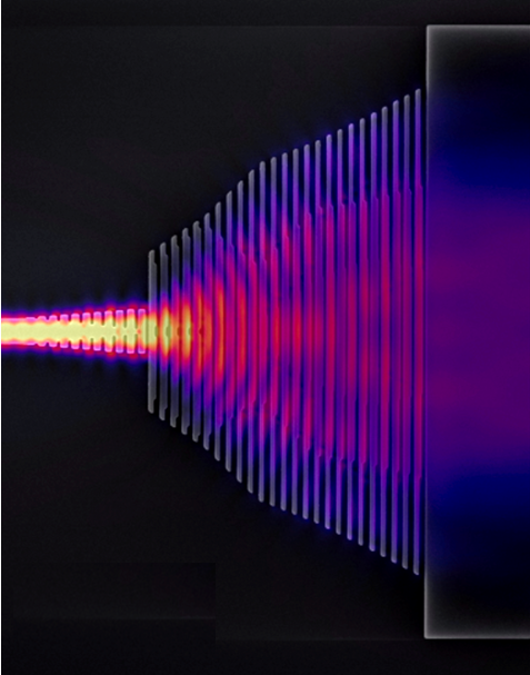
The resulting 2D structure was simulated with the finite-difference time-domain (FDTD) simulator Meep to obtain the device -parameters [see Figure 2(a)]. Each iteration consists of electromagnetic simulations run in parallel. The parameter was used to compute the score function for each candidate in the iteration, as defined in Equation 1. In the first iteration, the average insertion loss is , as shown in Figure 2(b). The insertion loss decreases progressively during the optimization, reaching after 100 2D iterations, beyond which no significant improvements are observed. Remarkably, substantial performance is achieved within the first 20 iterations, while subsequent iterations are devoted to fine-tuning the design for optimal results. The final iteration is considered the best 2D candidate (,) and serves as initialization for the optimization of the full 3D structure, using the LUT to map each homogeneous metamaterial cell into an SWG structure with the corresponding duty-cycle [see Figure 2(a)]. Notably the first 3D simulation already yields an average insertion loss of only , which is reduced to after 70 iterations – see Figure 2(b). The dimensions of the final design are given in Tables S1 and Table S2 of the supporting information. Figure 2(c) shows 3D FDTD of the final design in an extended 300 nm bandwidth, revealing that the spot-size-converter is extremely broadband. This is expected both from the compact size (7.2 µm including the input taper), as well as the broadband behavior of subwavelength structures. The average simulation time for each 2D simulation was 1.5 minutes, whereas each 3D simulation required approximately 1.2 hours. This two-stage approach is therefore crucial for accelerating the convergence of the optimization process. The simulations were performed on the Picasso supercomputer [34], equipped with thousands of CPU cores and high-memory nodes, allowing the parallelization of tasks and significantly reducing computational time.
3 Experimental results
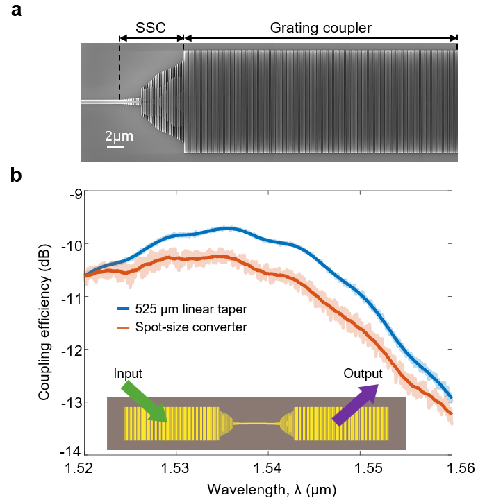
To experimentally demonstrate the proposed structure, a set of spot-size converters was fabricated on Applied Nanotools 220 nm-thick SOI platform using electron beam lithography [35]. A bias in the duty-cycle was introduced in the different test structures as defined in the inset of Figure 4(c) ( ). In our measurements light from a tunable laser (Santec TSL-770) was coupled into the chip using a lensed fiber and a polarization controller, through an SWG edge coupler [36]. The polarization controllers along with a Glan-Thompson polarizer at the output, allowed precise control of the polarization state within the chip. At the chip output, light was focused onto a photodetector using a microscope objective. The transmission spectrum was obtained by sweeping the wavelength of the tunable laser and recording the corresponding output power. Figure 4(a) presents the measurement data obtained by concatenating different numbers of devices for the nominal design, normalized to the transmission of a reference waveguide. The devices are arranged in a back-to-back configuration, as depicted in the inset, with a µm-long and 12 µm-wide waveguide between devices and a 150 µm-long single-mode waveguide between back-to-backs. These distances are chosen to ensure that the cavities formed by reflections from devices produce several oscillations within the 160 nm measurement bandwidth. To eliminate these oscillations, a minimum phase technique [37] has been applied in post-processing, which is shown as a solid line in Figure 4(a). The figure shows measurements for up to 40 concatenated devices (20 back-to-back structures), showcasing the robustness and performance of the design. Figure 4(b) depicts the linear regression at 1580 nm for three flavors, with the slope representing the estimated device losses, which are below 0.5 dB per device for the nominal design. Repeating this procedure across different wavelengths yields Figure 4(c), which shows the transmission as a function of wavelength for various biases. These results demonstrate that the devices can operate over a bandwidth of at least 160 nm with insertion losses below 0.8 dB.
To compare this performance with the state-of-the-art summarized in Table 1, we introduce the following figure of merit which incorporates the measurement bandwidth, device length and expansion factor:
| (3) |
A high FOM thus indicates a device that achieves a wide beam expansion over a broad bandwidth yet with a minimal length. As shown in Table 1, our spot-size converter improves on the state of the art by a significant margin, validating the potential of our metamaterial cell-based optimization approach.
As an additional verification, grating couplers were fed with our spot-size converter as shown in Figure 5(a). Identical gratings couplers fed by a 525 µm linear tapers were also fabricated to serve as a reference, as the losses for this taper length are negligible. We measured transmission when coupling in-and-out through a pair of gratings as shown in the inset of Figure 5(b), and calculated the coupling efficiency as the square root of this input-output transmission. As shown in Figure 5(b) the nominal SSC design yields a measured coupling efficiency difference compared to the lossless linear taper of less than . This difference corresponds with the losses of the SSC and is consistent with the back-to-back measurements shown in Figure 4(c). While a higher ripple due to reflections is observed, the overall length has been reduced by almost two orders of magnitude to 7.2 µm.
4 Conclusion
We have proposed a design methodology that leverages the optimization of cells of anisotropic subwavelength metamaterials to create a compact, high-performance spot-size converter. This design can expand a TE mode by a factor of 24 within a length of only 7.2 µm, with insertion loss below 0.8 dB across a measured bandwidth of 160 nm, thereby improving significantly on the state-of-the art. Indeed, our simulation predicts a potentially even larger bandwidth of 300 nm. This work serves as a proof of concept of the technique, demonstrating that it can produce high-performance device with very small footprints, which will be essential for future applications requiring high integration density, such as programmable and quantum photonics.
Supporting Information
Supporting Information is available from the Wiley Online Library or from the author. Data is available on Zenodo: https://doi.org/10.5281/zenodo.14640149.
Acknowledgements
We acknowledge funding through project PID2022-139540OB-I00 funded by MCIN/AEI
/10.13039/501100011033. A. S. S. acknowledges an FPI scholarship with reference PRE2022-000085.
References
- [1] S. Shekhar, W. Bogaerts, L. Chrostowski, J. E. Bowers, M. Hochberg, R. Soref, B. J. Shastri, Nature Communications 2024, 15, 1 751.
- [2] A. Torres-Cubillo, J. M. Luque-González, A. Sánchez-Postigo, A. Fernández-Gavela, J. G. Wangüemert-Pérez, Í Molina-Fernández, R. Halir, Journal of Lightwave Technology 2024, 42, 8 3010.
- [3] N. Li, C. P. Ho, J. Xue, L. W. Lim, G. Chen, Y. H. Fu, L. Y. T. Lee, Laser & Photonics Reviews 2022, 16, 11 2100511.
- [4] Y. Wang, S. Wang, R. Parsons, S. Sanyal, V. Gopal, A. Novick, A. Rizzo, M. Lipson, A. Gaeta, K. Bergman, IEEE Transactions on Components, Packaging and Manufacturing Technology 2024, 1–1.
- [5] E. Pelucchi, G. Fagas, I. Aharonovich, D. Englund, E. Figueroa, Q. Gong, H. Hannes, J. Liu, C.-Y. Lu, N. Matsuda, J.-W. Pan, F. Schreck, F. Sciarrino, C. Silberhorn, J. Wang, K. D. Jöns, Nature Reviews Physics 2021, 4, 3 194.
- [6] W. Bogaerts, D. Pérez, J. Capmany, D. A. B. Miller, J. Poon, D. Englund, F. Morichetti, A. Melloni, Nature 2020, 586, 7828 207.
- [7] S. D. Campbell, D. Sell, R. P. Jenkins, E. B. Whiting, J. A. Fan, D. H. Werner, Optical Materials Express 2019, 9, 4 1842.
- [8] S. Molesky, Z. Lin, A. Y. Piggott, W. Jin, J. Vuckovic, A. W. Rodriguez, Nature Photonics 2018, 12, 11 659.
- [9] C. M. Lalau-Keraly, S. Bhargava, O. D. Miller, E. Yablonovitch, Optics Express 2013, 21, 18 21693.
- [10] Z. Li, Z. Zhou, C. Qiu, Y. Chen, B. Liang, Y. Wang, L. Liang, Y. Lei, Y. Song, P. Jia, Y. Zeng, L. Qin, Y. Ning, L. Wang, Advanced Optical Materials 2024, 12, 7 2301337.
- [11] P. Cheben, R. Halir, J. H. Schmid, H. A. Atwater, D. R. Smith, Nature 2018, 560, 7720 565.
- [12] J. M. Luque-González, A. Sánchez-Postigo, A. Hadij-ElHouati, A. Ortega-Moñux, J. G. Wangüemert-Pérez, J. H. Schmid, P. Cheben, Í Molina-Fernández, R. Halir, Nanophotonics 2021, 10, 11 2765.
- [13] P. Cheben, J. H. Schmid, R. Halir, J. Manuel Luque-González, J. Gonzalo Wangüemert-Pérez, D. Melati, C. Alonso-Ramos, Advances in Optics and Photonics 2023, 15, 4 1033.
- [14] I. Staude, J. Schilling, Nature Photonics 2017, 11, 5 274.
- [15] J. M. Luque-González, R. Halir, J. G. Wangüemert-Pérez, J. de-Oliva-Rubio, J. H. Schmid, P. Cheben, Í Molina-Fernández, A. Ortega-Moñux, Laser & Photonics Reviews 2019, 13, 11 1900172.
- [16] X. Yi, C. Li, W. Zhao, L. Zhang, Y. Shi, D. Dai, Nanophotonics 2023, 12, 9 1809.
- [17] H. Xu, Y. Qin, G. Hu, H. K. Tsang, Laser & Photonics Reviews 2023, 17, 4 2200550.
- [18] R. Halir, P. Cheben, J. M. Luque-González, J. D. Sarmiento-Merenguel, J. H. Schmid, G. Wangüemert-Pérez, D. Xu, S. Wang, A. Ortega-Moñux, Í Molina-Fernández, Laser & Photonics Reviews 2016, 10, 6 1039.
- [19] J. Guo, L. Yu, H. Xiang, Y. Zhao, C. Liu, D. Dai, Advanced Photonics Nexus 2023, 2, 02.
- [20] H. Xu, Y. Qin, G. Hu, H. K. Tsang, Optics Letters 2023, 48, 2 327.
- [21] L. Moreno-Pozas, M. Barona-Ruiz, R. Halir, J. de Oliva-Rubio, J. Rivas-Fernández, I. Molina-Fernandez, J. G. Wangüemert-Pérez, A. Ortega-Moñux, Parabolic dielectric reflector for extreme on-chip spot-size conversion with broad bandwidth, 2025, URL http://arxiv.org/abs/2501.03206, ArXiv:2501.03206 [physics].
- [22] Y. Zhang, Y. He, H. Wang, L. Sun, Y. Su, ACS Photonics 2021, 8, 1 202.
- [23] Z. Wang, T. Li, A. Soman, D. Mao, T. Kananen, T. Gu, Nature Communications 2019, 10, 1 3547.
- [24] J. Zou, Y. Yu, M. Ye, L. Liu, S. Deng, X. Xu, X. Zhang, Optics Letters 2014, 39, 21 6273.
- [25] Y. Liu, W. Sun, H. Xie, N. Zhang, K. Xu, Y. Yao, S. Xiao, Q. Song, IEEE Journal of Selected Topics in Quantum Electronics 2019, 25, 3 1.
- [26] R. Liu, W. Zhao, D. Dai, Laser & Photonics Reviews 2024, 2301194.
- [27] W. Ma, M. Hou, R. Luo, B. Xiong, N. Liu, G. Liu, T. Chu, Nanophotonics 2023, 12, 6 1189.
- [28] Y. Wang, Y. Chen, K. Pan, S. Song, L. Li, X. Yi, In 2024 Photonics & Electromagnetics Research Symposium (PIERS). IEEE, Chengdu, China, ISBN 9798350375909, 2024 1–6, URL https://ieeexplore.ieee.org/document/10618022/.
- [29] N. Hansen, S. D. Müller, P. Koumoutsakos, Evolutionary Computation 2003, 11, 1 1.
- [30] N. Hansen, The CMA Evolution Strategy: A Tutorial, 2016, URL https://arxiv.org/abs/1604.00772, Version Number: 2.
- [31] C. Pérez-Armenta, A. Ortega-Moñux, J. Manuel Luque-González, R. Halir, P. J. Reyes-Iglesias, J. Schmid, P. Cheben, Í Molina-Fernández, J. G. Wangüemert-Pérez, Photonics Research 2022, 10, 4 A57.
- [32] S. Johnson, J. Joannopoulos, Optics Express 2001, 8, 3 173.
- [33] A. Herrero-Bermello, A. Dias-Ponte, J. M. Luque-González, A. Ortega-Moñux, A. V. Velasco, P. Cheben, R. Halir, Optics Express 2020, 28, 11 16385.
- [34] SCBI, Available at: https://www.scbi.uma.es/web/supercomputing/, URL https://www.scbi.uma.es/web/supercomputing/.
- [35] A. Nanotools, Available at: https://www.appliednt.com/, 2024, URL https://www.appliednt.com/.
- [36] P. Cheben, J. H. Schmid, S. Wang, D.-X. Xu, M. Vachon, S. Janz, J. Lapointe, Y. Painchaud, M.-J. Picard, Optics Express 2015, 23, 17 22553.
- [37] R. Halir, Í Molina-Fernández, J. G. Wangüemert-Pérez, A. Ortega-Moñux, J. de Oliva-Rubio, P. Cheben, Optics Express 2009, 17, 10 8349.
- [38] L. Pascar, D.-X. Xu, Y. Grinberg, S. Sajjanam Morrison, M. Vachon, O. Liboiron-Ladouceur, Optics Express 2024, 32, 16 28522.
| Table 1. Performance Comparison of SSC on SOI | |||||||||
| Structure | Ref | [µm] | [µm] | [µm] | [nm] | [nm] | [dB] | [nm] | |
| GRIN lens | [15] | 0.5 | 15 | 14 | <1 | >350 | <1 | >130 | 279 |
| Seg.taper | [24] | 0.5 | 12 | 20 | <0.5 | >60 | <0.7 | >45 | 54 |
| Topo. Opt | [25] | 0.5 | 10 | 5 | <1.5 | 40 | <1.5 | 40 | 160 |
| Luneburg lens1 | [22] | 0.5 | 10 | 11.2 | <1 | 740 | <1.5 | 220 | 393 |
| Metalens | [23] | 0.5 | 11 | 13.7 | <0.55 | 200 | <0.8 | 100 | 161 |
| Metalens Opt. | [38] | 0.5 | 15 | 10 | <1 | 40 | <1 | 40 | 120 |
| Topo. Opt. | [27] | 0.5 | 10 | 8 | <1 | 100 | <1 | 100 | 250 |
| Topo. Opt1 | [28] | 0.5 | 10 | 5 | <1 | 100 | <2.2 | 100 | 400 |
| Parabolic reflector | [20] | 0.45 | 10 | 32 | <0.2 | 200 | <0.15 | 100 | 69 |
| Achromatic lens1,2 | [26] | 2 | 10 | 26.2 | <0.56 | 300 | <0.4 | 200 | 38 |
| This work | - | 0.5 | 12 | 7.2 | <1 | 300 | <1 | 160 | 533 |
| 1Two-step etching process. | |||||||||
| 2Multiples modes | |||||||||
Table of Contents
See pages - of Supporting_Information.pdf