Polarization-induced Quantum Spin Hall Insulator
and Topological Devices in InAs Quantum Wells
Abstract
In this work, we predict the emergence of a quantum spin Hall insulator (QSHI) in conventional semiconductors, specifically InAs quantum wells, driven by a built-in polarization field. We propose QSHI InAs quantum wells as a platform to engineer topological field-effect devices. More precisely, we first present a novel topological logic device that operates without a topological phase transition. Subsequently, we design a high-performance topological transistor due to the presence of edge states. Our approach provides a potential framework for harnessing the unique features of QSHI in device design, paving the way for future topological devices.
Introduction.
Topological insulators are a novel class of materials distinguished by insulating bulk states and gapless conducting boundary states, which are protected by nontrivial topology Bansil et al. (2016). The in-depth development of topological band theory has spurred extensive research into topological materials Bradlyn et al. (2017); Po et al. (2017), revealing that about 24% of known materials exhibit topologically nontrivial phases Vergniory et al. (2019); Tang et al. (2019); Zhang et al. (2019). In particular, a two-dimensional (2D) quantum spin Hall insulator (QSHI) ensures the formation of robust edge states that enable dissipationless transport, making it promising for applications Narang et al. (2021); Qi and Zhang (2011). It is of particular interest for next-generation electronic devices due to their compatibility with the trend towards device miniaturization and the enhanced electrostatic control inherent in low-dimensional systems Fischetti et al. (2013); Jin et al. (2023); Weber et al. (2024).
Progress in topological devices Breunig and Ando (2022) has been largely limited to topological field-effect transistors (FETs) Qian et al. (2014); Vandenberghe and Fischetti (2017); Nadeem et al. (2021) and spintronics Chen et al. (2016); Huang et al. (2017); Acosta and Fazzio (2019), while topological logic devices are rare. Usually, the opening of the gap is essential to control the transport of topological devices Vandenberghe and Fischetti (2017). Therefore, a topological phase transition or finite-size effect is necessary Li and Chang (2009); Xu et al. (2019); Zhou et al. (2008); Ezawa and Nagaosa (2013). In order to improve performance at room temperature, topological devices rely on edge states, while bulk states need to be suppressed Breunig and Ando (2022). Consequently, a large bulk gap QSHI, such as 2D enes (=Bi, Sn and so on), is required in previous proprosals Molle et al. (2017). Furthermore, synthesizing high-quality samples of these materials poses challenges. To date, the electric-field-controlled topological phase transition has only been achieved in a few systems Bampoulis et al. (2023); Collins et al. (2018). How to effectively utilize the topological edge states of QSHI in device design remains an open question.
In this letter, we find that QSHI can be achieved in InAs quantum wells (QWs) with a nontrivial gap of 50 meV. Its band inversion is driven by a built-in electric polarization field. An effective Hamiltonian is obtained from ab-initio calculations. Then, we propose two types of topological devices based on InAs QWs: a NOR logic gate and a high-performance FET. In the NOR logic gate, which operates without a topological phase transition, the side gates are used to apply a transverse electric field to a narrow ribbon. In the FET device, the top split gate voltage is applied to regulate the effective width of the ribbon. Remarkably, its performance is comparable to that of state-of-the-art FETs.
Quantum spin Hall insulator in InAs quantum wells.
In experiments, [0001]-wurtzite/[111]-zincblende (WZ/ZB) InAs quantum wells are successfully grown Dick et al. (2010); Hjort et al. (2014); Staudinger et al. (2020). Due to the strain effect, a built-in polarization field is typically observed, reaching up to 4.90 MV/cm Dayeh et al. (2009); Li et al. (2014); Becker et al. (2018); Miao et al. (2012); Zhang et al. (2013, 2014). Here, we have systematically investigated the effect of the polarization field in WZ/ZB QWs. In our calculations, the QW structure consists of 2.1075 nm of WZ and 4.1932 nm of ZB InAs (in the direction) with the in-plane lattice constant nm (in the plane) as shown Fig. 1(a). Experiments demonstrate that the built-in polarization field is generated by the displacement of In atoms in the WZ structure along the [0001] direction, away from the center of the As4 tetrahedron Li et al. (2014). For simplicity, we shift In atoms in the WZ phase of the QW structure to simulate the polarization field.
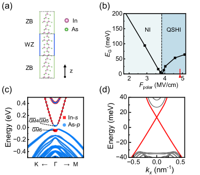
Fig. 1(b) shows the topological phase transition of InAs QWs as the built-in polarization field () varies in our first-principles calculations (see details in the Supplementary Materials (SM) (56) ). The built-in ( MV/cm) in QWs leads to band inversion and results in a QSHI. In the grown QW with =4.58 MV/cm Becker et al. (2018); Dick et al. (2010); Li et al. (2014), it belongs to a QSHI with a 53 meV nontrivial band gap. The band inversion is clearly shown by the orbital-resolved DFT band structure in Fig. 1(c). The index is calculated using the 1D Wilson loop method as implemented in the DFT package Zhang et al. (2023).
Furthermore, the irreducible representations of the low-energy bands are labeled as (In orbital) and (As orbitals) using IRVSP Gao et al. (2021), respectively. Based on these, the low-energy effective Hamiltonian and the parameters are obtained by VASP2KP Zhang et al. (2023) (see the SM (56) ). It is expressed as
| (1) |
where , , and . The parameters are eV, eV, , , , and . Accordingly, the topological helical edge states (red lines) are obtained in Fig. 1(d).
Design of topological devices in InAs QWs with electric field.
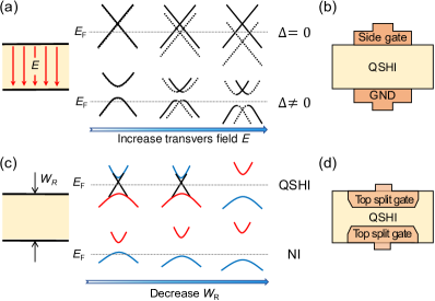
The topological helical states emerge on the edges of the QSHI ribbon. When the ribbon becomes sufficiently narrow, the two edge states can couple with each other, and a hybridization gap opens. A transverse electric field, applied through side gates, can easily adjust the energy level of the gap. To illustrate the mechanism clearly, we construct an effective model for the coupled 1D edge states. It reads as
| (2) |
where Pauli matrices and represent the spin space and the edge space. is the unit matrix. is the Fermi velocity. is the reduced Planck constant. The first term describes the topological helical edge states of the QSHI ribbon. The second term introduces the coupling strength between the two edges due to the finite-size effect. The third term describes the electrostatic potential () on one edge (the other edge is set to zero). For , although the energy levels of the edge states on one edge [dashed lines in Fig. 2(a)] decrease as increases, the system remains metallic without any gap. Once , a hybridization gap is induced, and its energy level changes as varies, as shown in Fig. 2(a). The system changes from a metallic state to an insulating state. This allows us to design a topological logic transistor with side gates of Fig. 2(b) without a topological phase transition.
Additionally, due to the thermal excitation, topological devices based on a narrow gap QSHI perform poorly at room temperature. Usually, a large gap QSHI is required Breunig and Ando (2022). Previous studies have shown that top split gates can regulate the effective width of the ribbons van Wees et al. (1988); Zhang et al. (2011); Wu et al. (2017). The evolutions of the band gap of the QSHI and NI are presented in Fig. 2(c) as varying the ribbon width (). In a 2D NI, there is always a band gap. However, a QSHI does not exhibit any gap in a relatively wide ribbon because of gapless edge states (black lines). This can result in a high current in the state of a topological FET. The state exhibits dissipationless transport in the presence of nonmagnetic disorder, even at room temperature. This makes the topological FET of Fig. 2(d) capable of achieving high performance at room temperature.
Topological NOR logic gate.
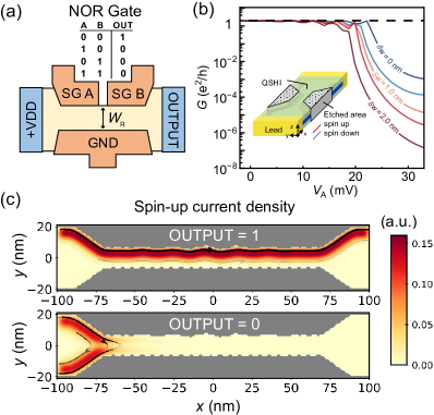
NOR/NAND logic gates are fundamental building blocks to perform complete logic operations in most logic systems Wakerly (2008), as all other logic operations can be derived from them. Based on the transverse field effect of coupled edge states in the QSHI, we propose a NOR logic gate that operates without a topological phase transition, as illustrated in Fig. 3(a). This logic gate utilizes coupled edge states with transverse electric fields applied through side gates (SG) A and B. In the state without voltage (logical inputs and ), the device is of a high-conductance state (logical output = 1). Most importantly, the output voltage is the same as the supply voltage due to the dissipationless transport of topological edge states. Applying a voltage ( or ) results in a low-conductance state (logical output = 0). Thus, it performs the complete NOR operation.
The device in Fig. 3(a) has a width = 12 nm, to induce a hybridization gap ( meV). Since SG A and SG B are in series, we only consider and keep in the numerical calculations (see the SM (56) ). As presented in Fig. 3(b), when , the calculated conductance is well-quantized at , which is consistent with the previous analysis that the topological edge states contribute to the quantized conductance. When meV is applied, the conductance is reduced to in the state, as the Fermi level is in the hybridization gap. Most interestingly, once rough boundary () is considered on the edges, the state is almost unchanged, as the topological edge states are robust against nonmagnetic impurities. However, in the state, the conductance is reduced to at nm, and to at nm. In other words, the rough boundary in the device can enhance the switching performance.
Fig. 3(c) presents only the spin-up component of the spin-resolved current density and its direction in both the and states of our device with nm. It is clearly observed that in the state, the spin-polarized topological edge state current flows along the rough boundary and is localized at the upper edge without backscattering. This also clearly reveals the spin-moment locking nature of the topological edge states. In the state, due to the coupling of opposite edge states, carrier tunneling occurs from the upper edge to the lower edge, significantly reducing the conductance between the left and right terminals. Thus, the current is completely blocked. This transverse-field-controlled transport is unique to QSHIs, as time-reversal symmetry ensures that backscattering occurs only through tunneling between the two edges. Using a transverse electric field, one can control the topological edge current, enabling electric-field-controlled topological logic.
Topological FET with top split gates.
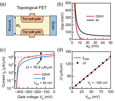
In addition to side gates, top split gates can also be used to regulate electron transport through the finite-size effect. We demonstrate that the existence of topological edge states in the width-tunable ribbon can significantly enhance the switching performance of a topological FET. In Fig. 4(a), we design a topological FET with top split gates, where the effective is controlled by the top gate voltage (). Experimental studies have found that varies linearly with over a wide range of 0 to 200 nm van Wees et al. (1988). Thus, it can be parameterized as , with the ribbon width and in Fig. 4. Fig. 4(b) illustrates the band gaps for the QSHI and the NI The NI is also described by the same Hamiltonian but with a different parameter meV to obtain a NI phase in this ribbon. with different . In the NI ribbon, there is always an energy gap. However, it starts to open an observable edge state gap () in the QSHI ribbon, when decreases to 15 nm. Once the becomes less than 15 nm, the gap increases rapidly.
In Fig. 4(c), we simulate the characteristic curves of the topological FET at room temperature ( = 300 K) and the source-drain voltage = 50 mV. The curve of a NI FET with the same device structure is marked by the blue line in Fig. 4(c) for comparison. The critical - (resp. -) state current of the FET is (resp. ). We can see that at the same gate voltage , the of the topological FET is higher. The gate voltage change required to switch the topological FET is approximately reduced by 50% compared to that of the NI FET. To quantitatively assess performance improvement, we introduce a commonly used performance metric in FETs: subthreshold swing Datta (2005). For conventional FETs at room temperature, the theoretical minimum is mV/decade Kim et al. (2020). The average subthreshold swing (current changes over ), in our devices, decreases from 69.5 mV/dec to 33.5 mV/dec, breaking the theoretical limit of subthreshold swing. This is comparable to advanced tunneling FET, negative-capacity FET Kamaei et al. (2023) and Dirac-source FET Liu et al. (2021).
It is worthwhile to notice the current difference between the topological FET and the NI FET. Fig. 4(c) shows that is 76.9 at mV. It corresponds to the topological edge current. We can compare with the current contributed solely by the topological edge state, , where . In Fig. 4(d), the numerical result of at different is shown. is close to at up to 100 mV. Although the bulk gap of this narrow gap QSHI is only about 50 meV, the contribution of the edge states can still be visualized at K. With nonmagnetic impurities, we conclude that the bulk current may be suppressed while the topological edge states in the state are preserved. Thus, topological FETs can maintain promising switching characteristics with nonmagnetic impurities. This suggests that a large bulk gap (e.g., over 100 meV) QSHI may not be necessary to achieve high-performance topological devices.
Discussion.
In this work, we find that the band structure can be tuned by the built-in electric polarization field of grown InAs QWs. Accordingly, a narrow-gap QSHI can be achieved with the experimental . We investigate the transport properties of the QSHI InAs ribbon with a field-controlled finite-size effect. Using the topological edge states of QSHI InAs QWs, we propose a topological logic without a topological transition and a high-performance topological FET even at room temperature. As device miniaturization continues, research on the transport properties in quasi-one-dimensional channels is an important topic for topological devices. Our finding provides new insight into the designs of the future topological devices.
The built-in polarization in the grown samples is widely found in narrow-gap III-V semiconductors. Besides the WZ/ZB InAs QWs Dick et al. (2010); Hjort et al. (2014), high-quality WZ/ZB InSb and built-in polarization are also obtained experimentally Anandan et al. (2019). Selective area epitaxy has enabled the fabrication of shape-controllable WZ/ZB InAs heterostructures Staudinger et al. (2020) and quantum well arrays Seidl et al. (2021). This makes these topological devices achievable. In addition, the previous examples of topological logic have recently been realized in acoustic and photonic systems Pirie et al. (2022); Zhang et al. (2022). The former relies on temperature and stress to control the topological phase, while the latter uses the phase difference of light. Our approach simplifies device design and integration by avoiding the complex conversion of physical quantities. Moreover, all inputs and outputs can be defined by the same supplied voltage in this topological NOR gate. This consistency in physical quantities facilitates the cascading of devices.
Acknowledgements.
This work was supported by the National Natural Science Foundation of China (Grants No. 12188101), National Key R&D Program of China (Grants No. 2022YFA1403800), and the Center for Materials Genome.
References
- Bansil et al. (2016) A. Bansil, H. Lin, and T. Das, Rev. Mod. Phys. 88, 021004 (2016), URL https://link.aps.org/doi/10.1103/RevModPhys.88.021004.
- Bradlyn et al. (2017) B. Bradlyn, L. Elcoro, J. Cano, M. G. Vergniory, Z. Wang, C. Felser, M. I. Aroyo, and B. A. Bernevig, Nature 547, 298 (2017), URL https://doi.org/10.1038/nature23268.
- Po et al. (2017) H. C. Po, A. Vishwanath, and H. Watanabe, Nature communications 8, 50 (2017), URL https://doi.org/10.1038/s41467-017-00133-2.
- Vergniory et al. (2019) M. Vergniory, L. Elcoro, C. Felser, N. Regnault, B. A. Bernevig, and Z. Wang, Nature 566, 480 (2019), URL https://doi.org/10.1038/s41586-019-0954-4.
- Tang et al. (2019) F. Tang, H. C. Po, A. Vishwanath, and X. Wan, Nature 566, 486 (2019), URL https://doi.org/10.1038/s41586-019-0937-5.
- Zhang et al. (2019) T. Zhang, Y. Jiang, Z. Song, H. Huang, Y. He, Z. Fang, H. Weng, and C. Fang, Nature 566, 475 (2019), URL https://doi.org/10.1038/s41586-019-0944-6.
- Narang et al. (2021) P. Narang, C. A. Garcia, and C. Felser, Nature Materials 20, 293 (2021), URL https://doi.org/10.1038/s41563-020-00820-4.
- Qi and Zhang (2011) X.-L. Qi and S.-C. Zhang, Rev. Mod. Phys. 83, 1057 (2011), URL https://link.aps.org/doi/10.1103/RevModPhys.83.1057.
- Fischetti et al. (2013) M. V. Fischetti, B. Fu, and W. G. Vandenberghe, IEEE Transactions on Electron Devices 60, 3862 (2013), URL https://doi.org/10.1109/TED.2013.2280844.
- Jin et al. (2023) K.-H. Jin, W. Jiang, G. Sethi, and F. Liu, Nanoscale 15, 12787 (2023), URL http://dx.doi.org/10.1039/D3NR01288C.
- Weber et al. (2024) B. Weber, M. Fuhrer, X.-L. Sheng, S. A. Yang, R. Thomale, S. Shamim, L. W. Molenkamp, D. H. Cobden, D. Pesin, H. J. Zandvliet, et al., Journal of Physics: Materials (2024), URL https://doi.org/10.1088/2515-7639/ad2083.
- Breunig and Ando (2022) O. Breunig and Y. Ando, Nature Reviews Physics 4, 184 (2022), URL https://doi.org/10.1038/s42254-021-00402-6.
- Qian et al. (2014) X. Qian, J. Liu, L. Fu, and J. Li, Science 346, 1344 (2014), URL https://www.science.org/doi/full/10.1126/science.1256815.
- Vandenberghe and Fischetti (2017) W. G. Vandenberghe and M. V. Fischetti, Nature communications 8, 14184 (2017), URL https://doi.org/10.1038/ncomms14184.
- Nadeem et al. (2021) M. Nadeem, I. Di Bernardo, X. Wang, M. S. Fuhrer, and D. Culcer, Nano Letters 21, 3155 (2021), URL https://pubs.acs.org/doi/full/10.1021/acs.nanolett.1c00378.
- Chen et al. (2016) W. Chen, W.-Y. Deng, J.-M. Hou, D. N. Shi, L. Sheng, and D. Y. Xing, Phys. Rev. Lett. 117, 076802 (2016), URL https://link.aps.org/doi/10.1103/PhysRevLett.117.076802.
- Huang et al. (2017) B. Huang, K.-H. Jin, B. Cui, F. Zhai, J. Mei, and F. Liu, Nature Communications 8, 1 (2017), URL https://doi.org/10.1038/ncomms15850.
- Acosta and Fazzio (2019) C. M. Acosta and A. Fazzio, Phys. Rev. Lett. 122, 036401 (2019), URL https://link.aps.org/doi/10.1103/PhysRevLett.122.036401.
- Li and Chang (2009) J. Li and K. Chang, Applied Physics Letters 95, 222110 (2009), URL https://doi.org/10.1063/1.3268475.
- Xu et al. (2019) Y. Xu, Y.-R. Chen, J. Wang, J.-F. Liu, and Z. Ma, Phys. Rev. Lett. 123, 206801 (2019), URL https://link.aps.org/doi/10.1103/PhysRevLett.123.206801.
- Zhou et al. (2008) B. Zhou, H.-Z. Lu, R.-L. Chu, S.-Q. Shen, and Q. Niu, Phys. Rev. Lett. 101, 246807 (2008), URL https://link.aps.org/doi/10.1103/PhysRevLett.101.246807.
- Ezawa and Nagaosa (2013) M. Ezawa and N. Nagaosa, Phys. Rev. B 88, 121401 (2013), URL https://link.aps.org/doi/10.1103/PhysRevB.88.121401.
- Molle et al. (2017) A. Molle, J. Goldberger, M. Houssa, Y. Xu, S.-C. Zhang, and D. Akinwande, Nature materials 16, 163 (2017), URL https://doi.org/10.1038/nmat4802.
- Bampoulis et al. (2023) P. Bampoulis, C. Castenmiller, D. J. Klaassen, J. van Mil, Y. Liu, C.-C. Liu, Y. Yao, M. Ezawa, A. N. Rudenko, and H. J. W. Zandvliet, Phys. Rev. Lett. 130, 196401 (2023), URL https://link.aps.org/doi/10.1103/PhysRevLett.130.196401.
- Collins et al. (2018) J. L. Collins, A. Tadich, W. Wu, L. C. Gomes, J. N. B. Rodrigues, C. Liu, J. Hellerstedt, H. Ryu, S. Tang, S.-K. Mo, et al., Nature 564, 390 (2018), ISSN 1476-4687, URL https://link.aps.org/doi/10.1038/s41586-018-0788-5.
- Dick et al. (2010) K. A. Dick, C. Thelander, L. Samuelson, and P. Caroff, Nano Letters 10, 3494 (2010), URL https://doi.org/10.1021/nl101632a.
- Hjort et al. (2014) M. Hjort, S. Lehmann, J. Knutsson, A. A. Zakharov, Y. A. Du, S. Sakong, R. Timm, G. Nylund, E. Lundgren, P. Kratzer, et al., ACS Nano 8, 12346 (2014), URL https://doi.org/10.1021/nn504795v.
- Staudinger et al. (2020) P. Staudinger, K. E. Moselund, and H. Schmid, Nano Letters 20, 686 (2020), URL https://doi.org/10.1021/acs.nanolett.9b04507.
- Dayeh et al. (2009) S. A. Dayeh, D. Susac, K. L. Kavanagh, E. T. Yu, and D. Wang, Adv. Funct. Mater. 19, 2102 (2009), URL https://doi.org/10.1002/adfm.200801307.
- Li et al. (2014) L. Li, Z. Gan, M. R. McCartney, H. Liang, H. Yu, W.-J. Yin, Y. Yan, Y. Gao, J. Wang, and D. J. Smith, Advanced Materials 26, 1052 (2014), URL https://onlinelibrary.wiley.com/doi/abs/10.1002/adma.201304021.
- Becker et al. (2018) J. Becker, S. Morkötter, J. Treu, M. Sonner, M. Speckbacher, M. Döblinger, G. Abstreiter, J. J. Finley, and G. Koblmüller, Phys. Rev. B 97, 115306 (2018), URL https://link.aps.org/doi/10.1103/PhysRevB.97.115306.
- Miao et al. (2012) M. S. Miao, Q. Yan, C. G. Van de Walle, W. K. Lou, L. L. Li, and K. Chang, Phys. Rev. Lett. 109, 186803 (2012), URL https://link.aps.org/doi/10.1103/PhysRevLett.109.186803.
- Zhang et al. (2013) D. Zhang, W. Lou, M. Miao, S.-c. Zhang, and K. Chang, Phys. Rev. Lett. 111, 156402 (2013), URL https://link.aps.org/doi/10.1103/PhysRevLett.111.156402.
- Zhang et al. (2014) H. Zhang, Y. Xu, J. Wang, K. Chang, and S.-C. Zhang, Phys. Rev. Lett. 112, 216803 (2014), URL https://link.aps.org/doi/10.1103/PhysRevLett.112.216803.
-
See Supplemental Materials for the details of DFT calculations, the Hamiltonian and the calculation of conductance and current with Refs. Kresse and Furthmüller 1996; Perdew et al. 1996; Kresse and Joubert 1999; Li et al. 2014; Ferreira et al. 2008; Mao et al. 2022; Dayeh et al. 2009; Hjort et al. 2014; Zhang et al. 2023; Gao et al. 2021; Datta 2005; Groth et al. 2014()SupplementalMaterials
See Supplemental Materials for the details of DFT calculations, the Hamiltonian and the calculation of conductance and current with Refs. Kresse and Furthmüller (1996); Perdew et al. (1996); Kresse and Joubert (1999); Li et al. (2014); Ferreira et al. (2008); Mao et al. (2022); Dayeh et al. (2009); Hjort et al. (2014); Zhang et al. (2023); Gao et al. (2021); Datta (2005); Groth et al. (2014).
- Zhang et al. (2023) S. Zhang, H. Sheng, Z.-D. Song, C. Liang, Y. Jiang, S. Sun, Q. Wu, H. Weng, Z. Fang, X. Dai, et al., Chinese Physics Letters 40, 127101 (2023), URL https://dx.doi.org/10.1088/0256-307X/40/12/127101,http://www.topmat.org/.
missing- Gao et al. (2021) J. Gao, Q. Wu, C. Persson, and Z. Wang, Computer Physics Communications 261, 107760 (2021), ISSN 0010-4655, URL https://www.sciencedirect.com/science/article/pii/S0010465520303805.
- van Wees et al. (1988) B. J. van Wees, H. van Houten, C. W. J. Beenakker, J. G. Williamson, L. P. Kouwenhoven, D. van der Marel, and C. T. Foxon, Phys. Rev. Lett. 60, 848 (1988), URL https://link.aps.org/doi/10.1103/PhysRevLett.60.848.
- Zhang et al. (2011) L. B. Zhang, F. Cheng, F. Zhai, and K. Chang, Phys. Rev. B 83, 081402 (2011), URL https://link.aps.org/doi/10.1103/PhysRevB.83.081402.
- Wu et al. (2017) Z. Wu, L. Lin, W. Yang, D. Zhang, C. Shen, W. Lou, H. Yin, and K. Chang, RSC Adv. 7, 30963 (2017), URL https://doi.org/10.1039/C7RA03482B.
- Wakerly (2008) J. F. Wakerly, Digital Design: Principles and Practices (Pearson Education, 2008).
- (42) The NI is also described by the same Hamiltonian but with a different parameter meV to obtain a NI phase in this ribbon.
- Datta (2005) S. Datta, Quantum Transport: Atom to Transistor (Cambridge university press, Cambridge, 2005).
- Kim et al. (2020) S. Kim, G. Myeong, W. Shin, H. Lim, B. Kim, T. Jin, S. Chang, K. Watanabe, T. Taniguchi, and S. Cho, Nature nanotechnology 15, 203 (2020), URL https://doi.org/10.1038/s41565-019-0623-7.
- Kamaei et al. (2023) S. Kamaei, X. Liu, A. Saeidi, Y. Wei, C. Gastaldi, J. Brugger, and A. M. Ionescu, Nature Electronics 6, 658 (2023), URL https://doi.org/10.1038/s41928-023-01018-7.
- Liu et al. (2021) M. Liu, H. N. Jaiswal, S. Shahi, S. Wei, Y. Fu, C. Chang, A. Chakravarty, X. Liu, C. Yang, Y. Liu, et al., ACS Nano 15, 5762 (2021), URL https://doi.org/10.1021/acsnano.1c01503.
- Anandan et al. (2019) D. Anandan, V. Nagarajan, R. K. Kakkerla, H. W. Yu, H. L. Ko, S. K. Singh, C. T. Lee, and E. Y. Chang, Journal of Crystal Growth 522, 30 (2019), URL https://www.sciencedirect.com/science/article/pii/S0022024819303367.
- Seidl et al. (2021) J. Seidl, J. G. Gluschke, X. Yuan, H. H. Tan, C. Jagadish, P. Caroff, and A. P. Micolich, ACS Nano 15, 7226 (2021), URL https://doi.org/10.1021/acsnano.1c00483.
- Pirie et al. (2022) H. Pirie, S. Sadhuka, J. Wang, R. Andrei, and J. E. Hoffman, Phys. Rev. Lett. 128, 015501 (2022), URL https://link.aps.org/doi/10.1103/PhysRevLett.128.015501.
- Zhang et al. (2022) F. Zhang, L. He, H. Zhang, L. Kong, X. Xu, and X. Zhang, Laser & Photonics Reviews 17, 2200329 (2022), URL https://onlinelibrary.wiley.com/doi/10.1002/lpor.202200329.
- Kresse and Furthmüller (1996) G. Kresse and J. Furthmüller, Computational Materials Science 6, 15 (1996), ISSN 0927-0256, URL https://www.sciencedirect.com/science/article/pii/0927025696000080.
- Perdew et al. (1996) J. P. Perdew, K. Burke, and M. Ernzerhof, Phys. Rev. Lett. 77, 3865 (1996), URL https://link.aps.org/doi/10.1103/PhysRevLett.77.3865.
- Kresse and Joubert (1999) G. Kresse and D. Joubert, Phys. Rev. B 59, 1758 (1999), URL https://link.aps.org/doi/10.1103/PhysRevB.59.1758.
- Ferreira et al. (2008) L. G. Ferreira, M. Marques, and L. K. Teles, Phys. Rev. B 78, 125116 (2008), URL https://link.aps.org/doi/10.1103/PhysRevB.78.125116.
- Mao et al. (2022) G.-Q. Mao, Z.-Y. Yan, K.-H. Xue, Z. Ai, S. Yang, H. Cui, J.-H. Yuan, T.-L. Ren, and X. Miao, Journal of Physics: Condensed Matter 34, 403001 (2022), URL https://dx.doi.org/10.1088/1361-648X/ac829d.
- Groth et al. (2014) C. W. Groth, M. Wimmer, A. R. Akhmerov, and X. Waintal, New Journal of Physics 16, 063065 (2014), URL https://dx.doi.org/10.1088/1367-2630/16/6/063065.
- Zhang et al. (2023) S. Zhang, H. Sheng, Z.-D. Song, C. Liang, Y. Jiang, S. Sun, Q. Wu, H. Weng, Z. Fang, X. Dai, et al., Chinese Physics Letters 40, 127101 (2023), URL https://dx.doi.org/10.1088/0256-307X/40/12/127101,http://www.topmat.org/.