suppSupplement
Topological phase diagram and quantum magnetotransport effects in (Pb,Sn)Se quantum wells with magnetic barriers (Pb,Eu)Se
Abstract
Despite several theoretical predictions regarding the physics and application of quantum wells (QWs) of topological crystalline insulators (TCI), no quantized charge transport via helical or chiral edge states has been experimentally demonstrated for such a class of systems. In this study, we report here on a successful growth by molecular beam epitaxy of high crystalline quality Pb1-xSnxSe:Bi/Pb1-yEuySe QWs with and , and on their magnetotransport characterization as a function of the QW thickness between 10 and 50 nm, temperatures down to 300 mK, perpendicular and tilted magnetic fields up to 36 T. The character of weak antilocalization magnetoresistance and universal conductance fluctuations points to a notably long phase coherence length. It is argued that a relatively large magnitude of the dielectric constant of IV-VI compounds suppresses the decoherence by electron-electron scattering. The observation of Shubnikov-de-Haas oscillations and the quantum Hall effect, together with multiband modelling, have enabled us to assess valley degeneracies, the magnitude of strain, subbands effective masses, the Berry phases, and the topological phase diagram as a function of the QW thickness. Our results demonstrate that further progress in controlling Sn content, carrier densities, and magnetism in Pb1-xSnxSe/Pb1-yEuySe QWs will allow for the exploration of the topologically protected quantized edge transport even in the absence of an external magnetic field. Furthermore, a reduced strength of electron-electron interactions will result in the absence of unpaired localized spins in the topological gap and, thus, in a substantially longer topological protection length compared to the quantum spin Hall materials explored so far.
I Introduction
In recent decades, the quantum Hall effects and other quantum transport phenomena have been observed in wide range of topological materials, including topological insulators, Dirac semimetals, and Weyl semimetals [1, 2, 3, 4]. However, one notable exception in this series is the topological crystalline insulators (TCIs) [5, 6, 7], which still lack experimental evidence for quantized edge resistance in either weak or high magnetic fields. In TCIs, the topological protection relies on the crystal point group symmetries [8]. The archetypical example of a TCI is SnTe [9], although this topological phase can also be achieved in other cubic IV-VI monochalcogenides with appropriately tuned compositions. The band structure of IV-VI semiconductors gives rise to distinct quantum Hall (QHE) features in these compounds [10, 11, 12], such as an unconventional sequence of filling factors [10] or the strain-controlled valley polarization in the 2D system [12]. The development of a robust TCI-based platform for quantum spin Hall (QSH) system would also allow experimentally access to the long-sought theoretical predictions, including the large-Chern-number quantum anomalous Hall effect (QAHE) [13, 14], topological transistor [15], and other phenomena unique to the thin TCI layers [16, 17]. Also recently IV-VI semiconductors have been considered an attractive platform for realising non-Abelian excitations [18, 19, 20, 21]. These advances could open new avenues for research and applications in the field of topological quantum materials.
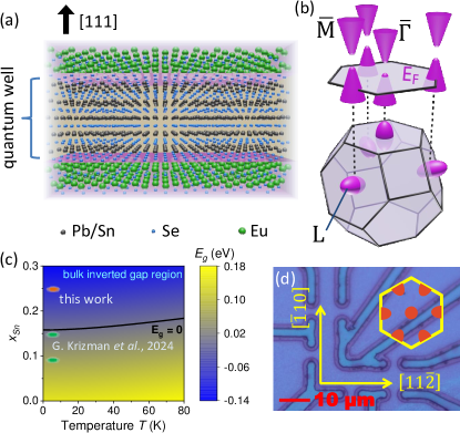
The choice of crystal orientation plays a critical role in determining the nature of surface states in TCIs [22]. Specifically, the growth orientation of a TCI-based 2D system defines the character of zero-field quantized edge transport [23, 24]. The most common growth orientations are and , which can be used for the realization of the 2D TCI phase or QSH, respectively. A typical substrate for epitaxial growth of IV-VI semiconductors is BaF2. As a result, in the 2D surface projection of band structure, the valence and conduction bands are close to each other at the point (commonly referred to as the longitudinal valley) and at the three inequivalent points (oblique valleys), as illustrated in Fig. 1. Pb1-xEuxSe(Te) is the preferred barrier material for Pb1-xSnxSe(Te) quantum well (QW) heterostructures, due to its closely matched lattice constants and thermal expansion coefficients. However, a residual lattice mismatch between the QW and the barrier materials affects the band gap and generates an energy offset between and bands [25, 26]. This offset is responsible for the unconventional sequence of QHE filling factors [10] and plays a key role in controlling valley polarization in these systems [12].
Previous magnetotransport studies of IV-VI QWs [27, 28, 10, 11, 12] have focused on samples with low Sn content, where the band inversion does not occur in the bulk crystal, and the TCI phase is absent. In this work, we report on a successful growth by molecular beam epitaxy of high crystalline quality Pb0.75Sn0.25Se:Bi/Pb0.9Eu0.1Se QWs with the thicknesses ranging from 10 to 50 nm. The achieved Sn content corresponds to the TCI phase in the bulk crystal. Longitudinal and Hall resistances of the patterned QWs have been studied at temperatures down to 300 mK and in perpendicular and tilted magnetic fields up to 36 T. In weak magnetic fields, we observe and interpret theoretically weak antilocalization (WAL) magnetoresistance and universal conductance fluctuations (UCF). We find that a relatively large magnitude of the dielectric constant results in weak decoherence by carrier-carrier scattering in IV-VI compounds, which enlarges WAL magnetoresistance and makes it possible to detect UCF in our 5 m-size Hall bars. The observation of Shubnikov-de-Haas (SdH) oscillations and the quantum Hall effect (QHE), together with multiband modelling, have allowed us to assess valley degeneracies, the magnitude of strain, subbands effective masses, the Berry phases, and the topological phase diagram as a function of the QW thickness. We argue that a large magnitude of the dielectric constant, resulting in a double occupation of localized states, may reduce scattering between helical edge states compared to the case of HgTe-type of topological insulators [29, 30]. In general terms, our results demonstrate that further progress in controlling Sn content, carrier densities, strain, and magnetism in Pb1-xSnxSe QWs will allow for the exploration of topologically protected quantized edge transport even in the absence of an external magnetic field with a prospect for quantum metrology applications.
II Samples and experimental
Following previous developments for IV-VI systems [12, 31, 32], molecular beam epitaxy (MBE) of Pb0.75Sn0.25Se/Pb0.9Eu0.1Se QWs studied here has been carried out on (111) BaF2 substrates using a Riber 1000 MBE system. The growth process was conducted in the ultra-high vacuum environment with a base pressure of mbar, utilizing compound PbSe and SnSe and elemental Eu and Se as the source materials. The composition of the QWs and barrier layers is determined by the beam flux ratio (SnSe/PbSe and PbSe/Eu), which is controlled by a quartz microbalance positioned at the substrate location. The substrate temperature was maintained at 350 ∘C and the growth rate was approximately 1 m/hour. The Pb0.9Eu0.1Se buffer and cap layers were grown to thicknesses of 2–3 m and 200 nm, respectively. To achieve low carrier densities and counterbalance the natural hole doping caused by Sn vacancies, extrinsic n-type Bi-doping (nominally 0.004%) was introduced using a Bi2Se3 doping cell. The sample surface quality is monitored in-situ using reflection high-energy electron diffraction (RHEED). Post-growth analyses, including atomic force microscopy (AFM) and X-ray diffraction (XRD), confirmed the high crystalline quality of the grown structures.
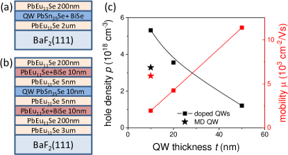
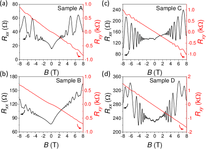
The current study focused on three Bi-doped QWs with thicknesses of 50, 20 and 10 nm, referred to as samples A, B and C, respectively, whose layout is shown in Fig. 2(a). A fourth sample (labelled as D), a 10 nm QW is modulation-doped, i.e., contains Bi-doped layers in the barriers, 5 nm away from the QW, as depicted in Fig. 2(b). Appendix B shows magnetoresistance and Hall effect measurements at 1.5 K obtained for unprocessed samples in a home-built 1.5 K/9 T setup. The low-field Hall slope and zero field resistivity indicate relatively low hole density, in the cm-3 range and the mobility values between 2 and 11 cm2/Vs, as summarized in Table 1 and in Fig. 2. In general, carrier mobility decreases with QW thickness, while the 2D carrier density remains nearly constant. Notably, a decrease in carrier density is also accompanied by increased mobility, as can be noted by comparing samples C and D.
| QW | , | (300 mK) | (300 mK) | ||||||||
|---|---|---|---|---|---|---|---|---|---|---|---|
| % | nm | % | cm-3 | cm-2 | cm2/Vs | cm-2 | cm-2 | m | m | ||
| A | 24 | 50 | 0.004 | 1.21 | 6.03 | 11400 | 4.50 | 4.08 | 2 3 | 1 | 6.0 |
| B | 25 | 20 | 0.004 | 3.56 | 7.13 | 4250 | 7.05 | 4.35 | 3 | 0.9 | 7.9 |
| C | 25 | 10 | 0.0042 | 5.32 | 5.32 | 1950 | 5.52 | 5.16 | 3 | 0.5 | 2.0 |
| D (MD) | 25 | 10 | 0.004 | 3.29 | 3.29 | 5900 | 3.28 | 2.82 | 3 | 0.7 | 3.0 |
The chosen heterostructures have been processed into L-shaped Hall bar structures (see Fig. 1(d)), using optical lithography and wet Br etching techniques. One arm of the Hall bar is aligned along the crystallographic direction, while the other — along the direction. This configuration allows for a comparison of transport properties when the current is applied either perpendicular or parallel to one of the oblique valleys. These structures were initially studied in moderate fields (up to 7 T) in the He3 cryostat, equipped with a piezoelectric rotator. Later, the same samples were investigated in high magnetic fields (up to 36 T) in the Grenoble High Magnetic Field Laboratory in a pumped helium cryostat, equipped with a manual rotator. In both setups, the rotators allow for the magnetic field tilt angle between 0∘ and 90∘, the perpendicular and in-plane configuration, respectively.
Table 1 shows the hole density determined for Hall bars from the low-field Hall resistance slope, compared to the value obtained from SdH oscillations, , where are the positions of the FFT peaks and the valley degeneracy for thinner QWs, as there are three oblique valleys occupied. For sample A, to account for spin degeneracy we use , as the spin splitting is not resolved in the FFT spectra. Overall, we can see that the carrier densities determined by both methods are consistent within approximately %, except for sample B. This discrepancy may be due to the presence of either a second subband or longitudinal valley at . Such factors could also explain the pronounced magnetoresistance and the low amplitude of SdH oscillations observed at low magnetic fields for this sample (see AppendixD).
III Results and Discussion
III.1 modelling and topological phase diagram
We have carried out computations of electric subbands and Landau levels in Pb0.75Sn0.25Se/Pb0.9Eu0.1Se QWs employing a four band model [33, 34, 35] taking into account the presence of confinement, strain, exchange interactions with Eu spins, and external magnetic field. We assume that except for the gap, the band structure parameters are independent of Sn and Eu content and . Further details about the Hamiltonian and computational method are provided in Appendix A.
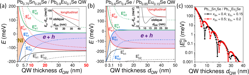
By plotting energy subbands as a function of QW thickness for various compositions, we can infer the transport properties for different compositions, thicknesses, and Fermi levels. For the composition used in the current work – Pb0.75Sn0.25Se/Pb0.9Eu0.1Se, shown in Fig. 3(a) – we see that below 5.7 nm, the system behaves a true insulator (shaded with orange). However, above this critical thickness, at the appropriate Fermi level, the system enters a mixed conduction state, with the contribution of both electrons and holes that originate from different valleys, as described in [12]. Although the bulk gap is inverted, in the heterostructure, the electron subbands are always above hole subbands for the corresponding valleys for reasonable values. The second subbands asymptotically tend to the values close to the bulk band edges at higher thicknesses.
The situation changes when we consider QWs with higher Sn content. For a QW with the composition Pb0.6Sn0.4Se/Pb0.85Eu0.15Se, Fig. 3(b), we clearly see the region where goes above . This indicates the gap inversion that occurs in the heterostructure and was previously described for QWs with higher Sn compositions [23, 24, 36]. However, in the current work, we consider this problem with a model based on experimental results and in a realistic environment. The current result agrees with previous works, as it also demonstrates: (i) the damped oscillatory behaviour of the gap in oblique valleys [23, 24], (ii) the absence of the gap inversion in the longitudinal valley [23, 24], and (iii) changes in the oscillation period with varying Sn content (Fig. 3(c)) [36]. Thus, the employed model can quantitatively reproduce previous experimental results and also agrees with previously published theoretical predictions obtained within the tight-binding approximation.
Inset in figure 3(a) show the band gaps at the and points without an external magnetic field as a function of the QW thickness for the Sn and Eu content used in the QWs studied in the current work. As expected, the confinement increases the band gap. Accordingly, the inverted order of bands, usually denoting the topological phase, is shifted to higher in QWs compared to the bulk case, from to depending on the value of (see Fig. 4a). These results imply that our QWs are in the normal phase, and should not show edge transport by helical states.
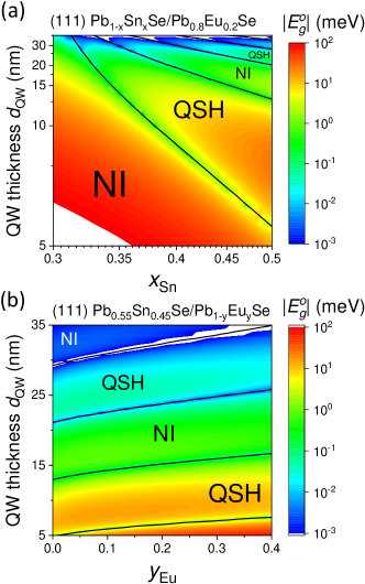
The described model can also be utilized to design TCI-based heterostructures to access topological edge transport. For instance, we can calculate the variation of the energy gap between and as a function of the Sn content in the QW (Fig. 4(a)) or as a function of Eu content in the barriers (Fig. 4(b)). Please note that in Fig. 4(a) QW thickness is presented on a reciprocal scale, while the Sn content is on a logarithmic scale. Over a wide range of parameters, the lines delimiting the gap inversion are very close to linear in these scales, providing a practical tool for evaluating the likelihood of observing gap inversion effects. However, accumulating more experimental data would help refine the values of the band parameters (Table 2) used in the model and better understand their dependence on composition. Additionally, a self-consistent expansion of the current model would enhance the precision of the results [37].
III.2 Weak antilocalization effect and universal conductance fluctuations
Figure 5 shows a pronounced, temperature dependent cusp in the negative weak-field magnetoconductance indicating the presence of the WAL effect, as found previously in thin epilayers [31] and QWs [38] of Pb1-xSnxSe and other narrow-gap semiconductors [39]. Additionally, aperiodic and reproducible fluctuations of , known as UCF, are also clearly visible in our Hall bridges with about 5 to 10 m distance between the contact probes.
We begin by describing the WAL effect employing the Hikami-Larkin-Nagaoka (HLN) expression for the case of strong SOC [40],
| (1) |
where the prefactor , where is a number of valleys uncoupled by inter-valley scattering; is the magnetic field perpendicular to the sample plane; is the digamma function; and is the dephasing field determined by the phase coherence length . We start by fitting at the lowest temperature K treating and as two adjustable parameters, though the presence of large fluctuations somewhat deteriorates the fit accuracy. With values obtained as an average of over that narrow temperature range, we determine in the whole studied temperature range up to 13 K. As shown in Figs. 5(e-h), magnitudes varies between 0.4 to almost 2 for between 8 and 2 m, respectively. Such correlation between and may indicate that intervalley scattering reduces to 1 in QWs with sufficiently large magnitudes of . Furthermore, temperature dependencies of summarized in Figs. 5(e-h), suggest the presence of two phase breaking mechanisms. Accordingly, we describe by the formula,
| (2) |
which takes into account dephasing by carrier-carrier scattering in the form expected for the 2D case and the electron-phonon dephasing process dominating at higher temperatures, . A relatively minor importance of dephasing by carrier-carrier scattering in IV-VI compounds results, as already noted [41, 31, 38, 42], from a sizable magnitude of the dielectric constant in systems close to a ferroelectric instability [43, 44].
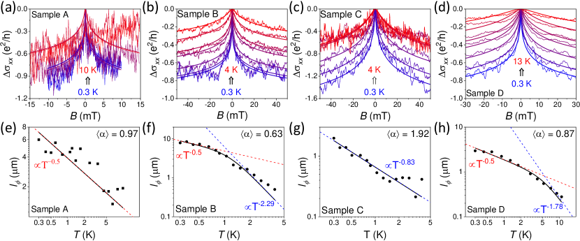
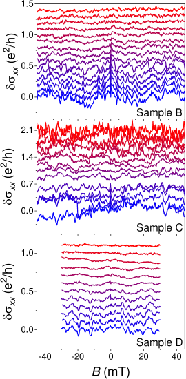
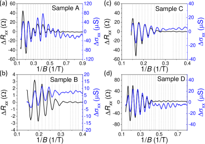
Turning to UCF, we show in Fig. 6 magnetoconductivity data after subtracting the WAL background, . Relatively large magnitudes of mean that the UCF magnitude is controlled by the thermal diffusion length [45, 46], , where in the 2D case is the diffusion coefficient, the values of and are given Table 1, , and according to SdH data discussed in the next section. For the determined parameters we see, that for all studied samples at the lowest temperature the and varies in the 0.5–1 m range (Table 1).
From the low-temperature amplitude of the UCF shown in Fig. 6, which is 0.07, 0.14 and 0.04 for samples B, C and D respectively, we can estimate [45, 46] the value from , where and are the linear dimensions of the Hall bar, typically 5 and 10 m’s, respectively (Fig. 1(d)). Assuming , spin degeneracy and the symplectic ensemble in weak magnetic fields or , and , i.e., the unitary ensemble in stronger fields we find 0.27, 0.35 and 0.13 m at 0.3 K for samples B, C and D respectively, which is by a factor of two smaller than expected from the value of . The value of can also be estimated from the half-width at the half-height of the autocorrelation function , which is expected to be [46] . Using this method, we obtain low-temperature of 0.5, 0.8 and 0.9 for samples B, C and D respectively, which is close to those estimated from the value of .
III.3 Quantizing Magnetic Fields
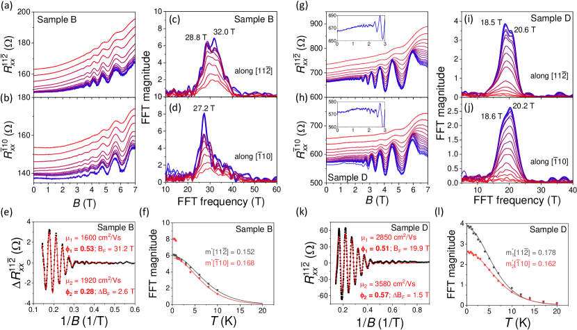
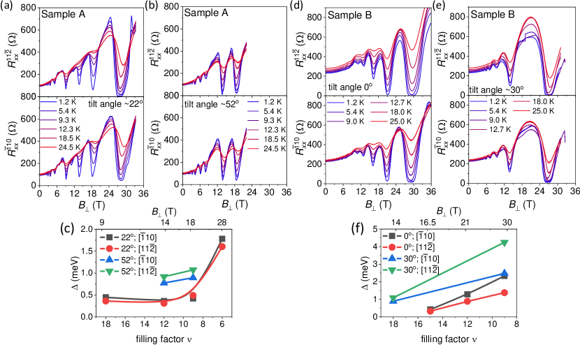
In the moderate field range, as shown in Figs. 7(a,b), we observe pronounced Shubnikov-de Haas (SdH) oscillations. They begin at approximately 0.5 T in the 50 nm-thick QW, indicating a large magnitude of the quantum lifetime and, thus, pointing to a high quality of the heterostructures. As in other systems [47], the values of quantum mobilities are lower than the weak-field Hall mobilities determined for the unprocessed QWs, shown in Table 1. As the QW thickness is reduced, both the quantum and Hall mobilities decrease significantly, underlying a crucial role of scattering at (Pb,Sn)Se/(Pb,Eu)Se interfaces. More specifically, the penetration of carriers’ wavefunction into (Pb,Eu)Se barriers allows for sizable alloy scattering by Eu cations, which significantly reduces the mobility [41]. The Coulomb interaction with background and remote impurities is likely less effective due to a high magnitude of the static dielectric constant in IV-VI semiconductors [34]. The oscillations’ pattern is virtually identical for the current along the [11] and [10] directions.
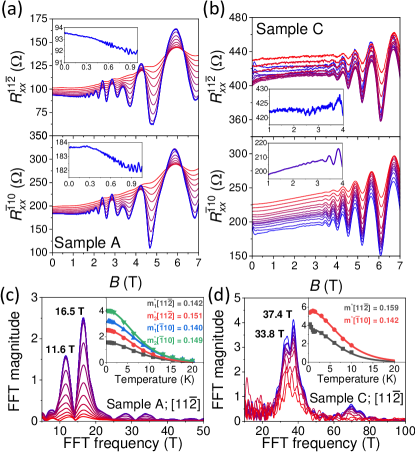
A notable feature is the oscillations’ beating pattern suggesting the presence of two frequencies. Indeed, after subtracting a smooth background, the fast Fourier transformation (FFT) revealed two main frequencies for sample A (Fig. 7(c,d)). However, for the sample C, a splitting is found only below 1 K. Similar splittings appear for two other samples (see Appendix D), which also correlate with the observation of the beating pattern. Spin-splitting persisting to low fields usually causes the beating pattern of the SdH oscillations. In our case, exchange interactions between carriers and barrier’s Eu dopants can result in additional low-field spin splitting [48] due to the penetration of the carrier’s wavefunction into the barriers. However, such splitting should depend strongly on temperature, which is not confirmed by the data. Another source of spin splitting is spin-orbit coupling (SOC) and inversion asymmetry [49, 50], as detected in IV-VI QWs by photoelectron spectroscopy [36]. The observation of weak antilocalization (WAL) in the studied QWs, as discussed in Sec. III.2, supports this interpretation. However, our calculations (Sec. III.4) show that while in thin (20 nm) QWs subbands are well separated, for thick (50 nm) QWs, the presence of two occupied subbands is likely, and could be responsible for the observed beating in sample A.
From temperature damping of the FFT peaks (Fig. 7(c,d)), we deduce the cyclotron mass of the carriers, using the temperature-dependent part of the Lifshitz-Kosevich equation [51]:
| (3) |
where is a fitting constant, is temperature, is the inverse of the mean value of the interval showing up in the FFT analysis, and is the cyclotron effective mass. Fitting the temperature dependence of the FFT peaks (insets in Figs. 7(c,d)) yields for the studied QWs, where is the free-electron mass. These values are close to the previously reported effective mass (0.13) for -type Pb0.7Sn0.3Se QW [38].
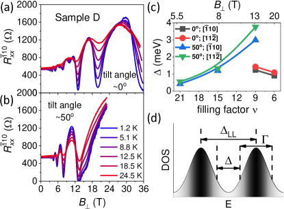
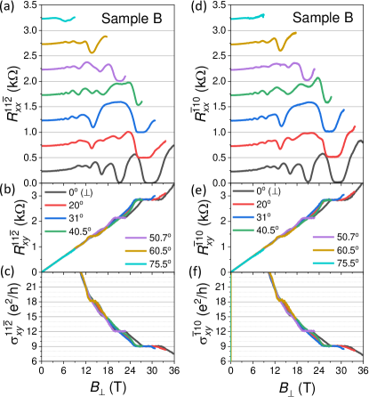
High-field experiments also revealed the presence of the quantum Hall effect (QHE). An example of QHE plateaus is shown in Fig. 8. The observed QHE filling factors, , are multiples of three, indicating that only oblique valleys contribute to the QHE and the spin degeneracy is removed. Notably, as the sample is tilted in the magnetic field, QH states at certain filling factors appear or disappear when varying the tilt angle. This occurs because the ratio of Zeeman to cyclotron energies changes with tilt.
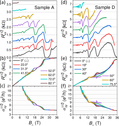
By analyzing the temperature dependence of the resistance minima in the QHE regime (Fig. 9(a,b)), we can evaluate an energy distance between the mobility edges in two subsequent LLs, according to , which is plotted in Fig. 9(c). However, results of the LLs calculations reveal that the Zeeman contribution becomes comparable with the cyclotron term at high fields [52, 53], and the resulting QH gaps should have almost a magnitude higher values (Fig. 10(c)). Such discrepancy points to the large LL broadening . The LL broadening can be determined through [47], where is a quantum lifetime. The is usually determined from the Dingle analysis of the low-field SdH oscillations. In our case, we fitted low-field SdH with a sum of two cosine functions:
| (4) |
where are fitting constants, are quantum mobilities corresponding for each frequency, is the main frequency and determines the splitting of the main frequency, finally are phase shifts for each frequency peak. After fitting the SdH oscillations at the lowest temperature, the obtained values for and were similar to those acquired from the FFT analysis. The results of the SdH fittings and the corresponding values of , as well as the oscillation’s phase analysis, are shown and discussed in more detail in Appendix D. Quantum lifetimes have similar values for all QWs and fall to the range of 0.14–0.44 ps, corresponding to the –15 meV. Thus, all three energy scales (Fig. 9d) are in qualitative agreement with each other.
Also, according to the model (see Appendix A), for the samples with a single occupied subband, odd should correspond to the pure Zeeman gap which also includes exchange term (), while even – to the difference between cyclotron and Zeeman gaps (). While changing the tilt angle, the Zeeman contribution remains constant (increases) with (), while cyclotron energy reduces (remains constant) with (). According to such a naive picture, the energy gaps for odd ’s should decrease, and for even ’s – increase. Nevertheless, in the -type PbSnSe QWs situation is the opposite due to the role of exchange contribution to the Zeeman energy (see Appendix A). Numerical simulations show only limited qualitative agreement between experimental and theoretical results.
III.4 SdH fitting with model
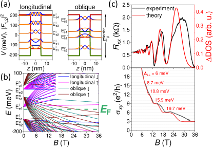
By diagonalizing the Hamiltonian in zero magnetic fields, we obtained subbands’ wavefunctions – the Kramers doublet (Appendix A), whose squared modulus is shown in Fig. 10(a). Here we can see that the wavefunction’s tails penetrate the barriers. As already mentioned, this penetration results in strong alloy scattering reducing mobility values in thin QWs and in a non-zero exchange interaction between the carriers and Eu spins, similar to the Mn-doped barriers of the DMS QWs [54]. Exchange spin-splittings are crucial for the appearance of the quantum anomalous Hall effect in topological matter [55, 13, 56]. By incorporating the exchange interactions into the Hamiltonian, we are able to quantitatively describe the SdH oscillations in sample D. The corresponding LL diagram is shown in Fig. 10(b). The resulting LLs are non-linear, with a distance between individual LLs being of the order of 10-30 meV. At the Fermi level, meV, we computed both density of states (DOS) oscillations and the Hall conductivity, as illustrated in Fig. 10(c). Such lies between and and only is occupied (Fig. 3a), which is consistent with the observation of the p-type carriers and with the degeneracy of the observed QH states. The resulting DOS oscillations closely match the experimental data, highlighting the model’s quantitative accuracy and its capability to provide insights into the band structure of IV-VI quantum wells under realistic experimental conditions. This means it can be used to analyse the experimental data and foresee ways to improve the heterostructure design for specific needs. Meanwhile, due to the lack of detailed knowledge on how band parameters vary with the Sn content and other assumptions made in the calculations, we could not quantitatively reproduce results from thicker QWs. However, this issue falls outside the scope of the current work.
IV Summary
In summary, we found several quantum features in hole transport in QWs of Sn-rich (Pb,Sn)Se with a relatively large inverted bulk band gap. The observed and quantitatively interpreted phenomena include WAL magnetoresistance, aperiodic UCF, SdH oscillations, and the quantum Hall effect. The observation of the QHE plateaus represents a significant step forward in the development of TCI heterostructures showing high Chern number QAHE states. The obtained results illustrate the interplay of strain, confinement, spin-orbit coupling, exchange interaction with barrier Eu spins, and multi-valley physics in the vicinity of the topological phase transition. To interpret our findings, we numerically solved Hamiltonian, which has allowed us to quantitatively reproduce the experimental data for narrow QWs. This approach has the potential to quantitatively predict and describe other magnetotransport phenomena with precision comparable to that achieved for HgTe QWs [57, 58, 37].
Our work also highlights challenges and opportunities for future progress. The (Pb,Eu)Se barrier material employed in this study introduces significant strain, such that the gaps of the longitudinal and oblique valleys do not coincide. While this strong partial lifting of valley degeneracy may have potential applications in valleytronics [12], it also hinders the realization of quantized topological conduction by causing the hybridization of the helical or chiral edge channels with bulk carriers. One of the possible ways to overcome such a situation would be to engineer the barrier materials carefully. A potential candidate for the barrier material would be the EuxSr1-xSySe1-y compound [59, 60], which offers simultaneous control over lattice constant, energy gap, and magnetism in the desired range. In more general terms, our work constitutes a worthwhile step towards achieving exotic topological phases in TCI-based heterostructures through advances in chemical, strain, and quantum structure engineering as well as enlarges the way for demonstrating non-Abelian excitations in topological nanowires and improving figures of merit of thermoelectric junctions, infrared lasers and detectors that do not contain critical elements, like Ga and In.
Acknowledgments
The authors thank Günther Bauer and Gauthier Krizman for valuable discussions. This research was partially supported by the Foundation for Polish Science project ”MagTop” no. FENG.02.01-IP.05-0028/23 co-financed by the European Union from the funds of Priority 2 of the European Funds for a Smart Economy Program 2021-2027 (FENG) and by Narodowe Centrum Nauki (NCN, National Science Centre, Poland) IMPRESS-U Project No. 2023/05/Y/ST3/00191. V.V.V. also acknowledges long-term program of support of the Ukrainian research teams at the Polish Academy of Sciences carried out in collaboration with the U.S. National Academy of Sciences with the financial support of external partners. Measurements at high magnetic fields were supported by LNCMI-CNRS, members of the European Magnetic Field Laboratory (EMFL) and by the Ministry of Education and Science, Poland (grant no. DIR/WK/2018/07) via its membership to the EMFL. Publication subsidized from the state budget within the framework of the programme of the Minister of Science (Polska) called Polish Metrology II project no. PM-II/SP/0012/2024/02.
Author contributions
V.V.V. grew the heterostructures with the assistance of G.S. and carried out structural characterization; A.K. carried out microstructure processing and all magnetotransport measurements with the assistance of Z.A.; C.-W.C. and B.A.P. assisted in high-field magnetotransport measurements. T. Wojciechowski performed an EDX analysis and assisted in microstructure processing. A.K. and T.D. performed calculations. T. Wojtowicz and T.D. were responsible for funding acquisition and general management. The manuscript was written by A.K., V.V.V., B.A.P., and T.D. All authors discussed the results and commented on the manuscript.
Appendix A model
A.1 Low magnetic fields
We start with the four band Hamiltonian [33, 34, 35]:
| (5) |
Here, is aligned along the growth direction, i.e., [111]; , , gives Zeeman splitting with respect to the tilted magnetic field. Other band parameters are listed in Table 2 and taken as constants throughout the heterostructure. We assume that changes in the band parameters over the interface are negligible because of (i) a small level of Eu- and Sn- alloying relative to the parent PbSe compound and (ii) the low penetration amplitude of the resulting wavefunctions into the barrier. However, we used a slightly different set of band parameters for the longitudinal and oblique valleys.
Additionally, we introduce also the - exchange interaction between band carriers and Eu ions residing in the barriers. We consider only the exchange term for holes, as exchange coupling is small for electrons [35, 61]. We added the following term to the initial Hamiltonian:
| (6) |
Here, are versors describing the direction of the total magnetic field ; , where is the Eu content in the barriers, meV is the exchange energy, and is Eu spin. is the Brillouin function with an argument , where is the Eu spin -factor.
We assume band offsets to change across the (Pb,Sn)Se/(Pb,Eu)Se interface according to,
| (7) |
where ’’ sign is chosen for conduction () bands and ’’ – for the valence () bands. Here, is the energy gap of the QW material, and of the barrier material. QW energy gap is determined from [34]:
| (8) |
and the barrier energy gap is determined from [62]:
| (9) |
Here we also include the effect of strain on the band structure [63], by considering term. We assume that the barriers are completely relaxed and the strain in the QW is determined by the ratio between the corresponding lattice constants [63, 26]:
| (10) |
where is lattice constant of unstrained QW material [53]:
| (11) |
and is the lattice constant of the barrier material [12]:
| (12) |
Since here comes the ratio between lattice constants, we do not consider the effect of the thermal expansion following the reasoning provided in [26]. Then, the out-of-plane strain is [63]:
| (13) |
where elastic constants , , and are 14.18, 1.94, and 1.749, respectively [63]. The strain shifts the band edges of the material differently for longitudinal and oblique valleys [26]:
| (14) | |||
| (15) |
Values for the deformation potentials were taken from [63] and slightly adjusted to better match the published experimental data on the dispersion and oblique/longitudinal valley offsets [36, 12], Table 3. Thus, to account for the strain effect, substitutes and the corresponding Schrödinger problem:
| (16) |
is solved separately for the longitudinal and oblique valleys. The eigenvector is expanded as:
| (17) |
where is between 50 and 100 to ensure an appropriate numerical convergence, is the total thickness of the considered structure.
At zero magnetic field () and zero momentum (), can be reduced to two eigenvalue problems:
| (18) | ||||
Here, and are valence and conduction components of the wavefunction for the ’th subband.
| valley | [m/s] | ||||||||
|---|---|---|---|---|---|---|---|---|---|
| l | 0.37 | 0.20 | 0.37 | 0.20 | -3.3 | -0.8 | -5.1 | -3.5 | |
| o | 0.08 | 0.09 | 0.08 | 0.09 | -3.89 | -0.94 | -6.01 | -4.13 |
| -4.36 | 8.29 | -8.93 | 10.46 |
A.2 High magnetic fields
To account for the quantizing magnetic fields, we substitute and :
| (19) | |||
| (20) |
where and are annihilation and creation operators for the harmonic oscillator , thus . This leads to the following Hamiltonian :
| (21) |
where is the cyclotron frequency. We have not considered here the effect of the in-plane magnetic field mixing spatial and momentum variables [64]. Then, the Landau levels are calculated up to = 30 using the same approach as described above. Note, that the LL is spin polarized in the case of an inverted gap since the topological surface states form it [52].
The oscillations of the density of states (DOS) at the Fermi level are estimated through:
| (22) |
where describes Landau-level broadening.
Such a simplified picture nevertheless captures the general trend of the magnetic field tilt angle dependence of the SdH oscillations. In Fig. 11 we compared experimental results (upper panel) with the outcome of numerical modelling (lower panel). Indeed, according to the naive picture, the energy gaps for the even ’s should increase with a tilt angle as a function of , since they are purely Zeeman gaps. This is not the case either for experimentally measured curves or for the results of the calculations. Further investigation reveals that the faster closing of the Zeeman gap with increasing tilt angle is primarily driven by exchange interactions. Nonetheless, a more detailed and comprehensive model is required to fully explain this behavior.
Appendix B Magnetoresistance data for unprocessed quantum wells
The results of the initial characterization of the studied QWs are presented in Fig. 12.
Appendix C Thermal cycling and illumination
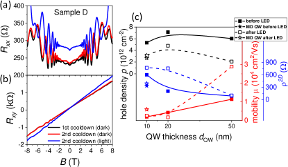
Previously, it was found that repeated exposure to temperature variations causes structural flaws to develop in IV-VI compound layers due to differences in their expansion properties compared to the substrate. This leads to an increase in carrier density and degradation in the material’s electrical transport characteristics [28]. To assess the impact of thermal cycling on transport properties, we compared two successive cooldowns (Fig. 13(a,b), black and red curves). We found that thermal cycling has a negligible effect on carrier density and slightly deteriorates mobility. The curves in Fig. 13(a,b) were measured on unprocessed samples, however, the same behavior was observed in the Hall-bar samples, discussed in the main text.
Another common phenomenon in 2D semiconductor heterostructures is the persistent photoconductivity (PPC) effect. Indeed, such an effect was observed in the IV-VI heterostructures [65, 66], where significant changes in the carrier density were reported. In our study of (Pb,Sn)Se/(Pb,Eu)Se QWs, we also observe the PPC effect; see red and blue lines on Fig. 13(a,b). The measurement protocol has been as follows: starting from 1.6 K, the sample was warmed up to 20 K and a green LED was turned on with a 5 A current for 1 hour until stabilized. After that, the LED was turned off, and the sample remained for 1 hour in the dark. The sample was then cooled back down to 1.6 K, and magnetotransport measurements were taken. The hole density decreased from 3.28 to 2.67 1012 cm-2, while the mobility increased slightly by 1.5 %. According to previous studies [65], the PPC effect originates from the excitation of the charges from the trap levels associated with Eu atoms. However, the role of interfacial defects cannot be excluded.
Appendix D Additional data for the SdH oscillations and phase analysis
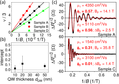
An important question which often arises in the analysis of quantum oscillations in topological materials is the phase offset in the SdH oscillations. It is believed that for a topological 2D system, should include an additional Berry phase shift. Usually, a Landau fan diagram is plotted to determine the phase shift in the system under study. From the QHE states, we can construct an LL fan diagram (Fig. 14(a)) by plotting vs. the inverse perpendicular component of the magnetic field . Here we have divided by three to account for valley degeneracy. Fitting linear dependence yields almost zero intercepts for all QWs (Fig. 14(b)). However, it was claimed that this method tends to give imprecise values of [67]. An alternative approach to extract the phase offsets is to fit the oscillations with a sum of two cosine functions (see main text). For all studied QWs, the values of significantly differ from zero for both cosine terms. However, only samples A and D exhibit close to the quantized value of 0.5. In other QWs, phase offsets are essentially non-zero but not quantized.
It was previously shown [68, 69] that even if , one should be careful in concluding about the topological nature of the material. Moreover, it was claimed [67] that the phase offset in 2D systems cannot be directly linked to the Berry curvature, and consequently to the topological nature of the material. However, one can naively argue that characterises the closed gap (semimetallic) in a thicker QW, while thinner QW might be considered as trivial insulators or to 2D system with a strong SOC, as indicated by calculations.
Additional data on the low-field ( T) SdH oscillations for samples B (Fig. 15(a-f)) and D (Fig. 15(g-l)). These include raw and measurements, as well as FFT analysis, cyclotron fitting and two-cosine fitting of the .
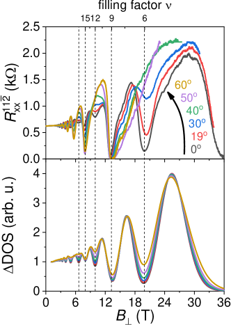
Appendix E Tilt angle dependence in moderate fields
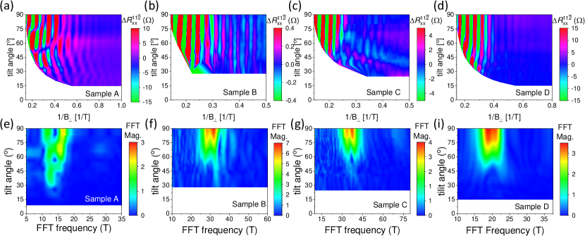
In 2D (3D) systems, the frequency of SdH oscillations remains unchanged as a function of (). However, variations in the SdH pattern can occur due to changes in the ratio between cyclotron and Zeeman energies in 2D systems or due to band anisotropy in 3D systems. We have performed tilted field experiments for all the studied QWs (Fig. 16). We find that the main frequency remained constant as a function of a tilt angle, which is consistent with a 2D nature of the magnetotransport of the QWs. Meanwhile, we have observed that the field tilting changes the value in some samples.
Appendix F Additional data for the QHE
The section contains data on the high-field QHE for samples A (Fig. 17 and 18) and B (Fig. 18). These include raw and measurements, as well as temperature evolution of the QHE states at two tilt angles and results of their temperature damping analysis, that gives an estimation of the thermal activation gap .
Appendix G QW’s in a parallel magnetic field
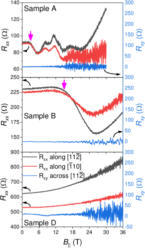
Being a 2D system, the quantum well should not exhibit oscillations in the parallel field. As for low magnetic fields, we have shown that this is the case. However, for high magnetic fields, when the magnetic length becomes comparable or lower than the QW width, the 2D gas may exhibit quantum oscillations. Indeed, if we consider QW behavior in 36 T in-plane magnetic fields we see resistance oscillations for samples A and B (Fig.19). In low magnetic fields of several Teslas, we see small positive magnetoresistance, which interrupts with abrupt turndown. We can compare the onset of this turndown in magnetic length units with the QW’s thickness. This onset is 3 T and 15 T for sample A and B respectively. These magnetic fields correspond to 14.8 nm and 6.6 nm, about 1/3 of the QW width for both thicknesses. For sample D, this ratio of 1/3 gives an estimation of 60 T for the onset of the oscillations, which lies beyond the range of fields, employed within our study.
Appendix H Comparison between SdH oscillations in and
Previously, it was shown and discussed [70, 4] that the phase of the oscillations should be accurately extracted from the , rather than from . To validate that extracting phase from the fitting of is appropriate, we compare the SdH oscillations in and , see Fig. 20. As shown, the positions of the minima and maxima of the oscillations coincide, indicating that the phase offset between and is negligible. This is a consequence of the fact that we are working with a 2D system, where magnetotransport oscillations are much more pronounced, and low values of the carrier densities.
References
- Zhang et al. [2005] Y. Zhang, Y.-W. Tan, H. L. Stormer, and P. Kim, Nature 438, 201 (2005).
- Büttner et al. [2011] B. Büttner, C. X. Liu, G. Tkachov, E. G. Novik, C. Brüne, H. Buhmann, E. M. Hankiewicz, P. Recher, B. Trauzettel, S. C. Zhang, and L. W. Molenkamp, Nature Physics 7, 418 (2011).
- Xu et al. [2014] Y. Xu, I. Miotkowski, C. Liu, J. Tian, H. Nam, N. Alidoust, J. Hu, C.-K. Shih, M. Z. Hasan, and Y. P. Chen, Nature Physics 10, 956 (2014).
- Qiu et al. [2020] G. Qiu, C. Niu, Y. Wang, M. Si, Z. Zhang, W. Wu, and P. D. Ye, Nature Nanotechnology 15, 585 (2020).
- Dziawa et al. [2012] P. Dziawa, B. J. Kowalski, K. Dybko, R. Buczko, A. Szczerbakow, M. Szot, E. Łusakowska, T. Balasubramanian, B. M. Wojek, M. H. Berntsen, O. Tjernberg, and T. Story, Nature Materials 11, 1023 (2012).
- Tanaka et al. [2012] Y. Tanaka, Z. Ren, T. Sato, K. Nakayama, S. Souma, T. Takahashi, K. Segawa, and Y. Ando, Nature Physics 8, 800 (2012).
- Xu et al. [2012] S.-Y. Xu, C. Liu, N. Alidoust, M. Neupane, D. Qian, I. Belopolski, J. Denlinger, Y. Wang, H. Lin, L. Wray, G. Landolt, B. Slomski, J. Dil, A. Marcinkova, E. Morosan, Q. Gibson, R. Sankar, F. Chou, R. Cava, A. Bansil, and M. Hasan, Nature Communications 3, 10.1038/ncomms2191 (2012).
- Fu [2011] L. Fu, Physical Review Letters 106, 106802 (2011).
- Hsieh et al. [2012] T. H. Hsieh, H. Lin, J. Liu, W. Duan, A. Bansil, and L. Fu, Nature Communications 3, 982 (2012).
- Chitta et al. [2005] V. A. Chitta, W. Desrat, D. K. Maude, B. A. Piot, N. F. Oliveira, P. H. O. Rappl, A. Y. Ueta, and E. Abramof, Physical Review B 72, 195326 (2005).
- Pena et al. [2021] F. S. Pena, S. Wiedmann, E. Abramof, D. A. W. Soares, P. H. O. Rappl, S. de Castro, and M. L. Peres, Physical Review B 103, 205305 (2021).
- Krizman et al. [2024] G. Krizman, J. Bermejo-Ortiz, T. Zakusylo, M. Hajlaoui, T. Takashiro, M. Rosmus, N. Olszowska, J. J. Kołodziej, G. Bauer, Y. Guldner, G. Springholz, and L.-A. de Vaulchier, Physical Review Letters 132, 166601 (2024).
- Fang et al. [2014] C. Fang, M. J. Gilbert, and B. A. Bernevig, Physical Review Letters 112, 10.1103/physrevlett.112.046801 (2014).
- Niu et al. [2015] C. Niu, P. M. Buhl, G. Bihlmayer, D. Wortmann, S. Blügel, and Y. Mokrousov, Physical Review B 91, 201401 (2015).
- Liu et al. [2013a] J. Liu, T. H. Hsieh, P. Wei, W. Duan, J. Moodera, and L. Fu, Nature Materials 13, 178 (2013a).
- Tang and Fu [2014] E. Tang and L. Fu, Nature Physics 10, 964 (2014).
- Li et al. [2016] X. Li, F. Zhang, and A. H. MacDonald, Physical Review Letters 116, 026803 (2016).
- ten Kate et al. [2022] S. C. ten Kate, M. F. Ritter, A. Fuhrer, J. Jung, S. G. Schellingerhout, E. P. A. M. Bakkers, H. Riel, and F. Nichele, Nano Letters 22, 7049 (2022).
- Gomanko et al. [2022] M. Gomanko, E. J. de Jong, Y. Jiang, S. G. Schellingerhout, E. Bakkers, and S. Frolov, SciPost Physics 13, 089 (2022).
- Schellingerhout et al. [2023] S. G. Schellingerhout, R. Bergamaschini, M. A. Verheijen, F. Montalenti, L. Miglio, and E. P. Bakkers, Advanced Functional Materials 10.1002/adfm.202305542 (2023).
- Song et al. [2023] W. Song, Y. Wang, W. Miao, Z. Yu, Y. Gao, R. Li, S. Yang, F. Chen, Z. Geng, Z. Zhang, S. Zhang, Y. Zang, Z. Cao, D. E. Liu, R. Shang, X. Feng, L. Li, Q.-K. Xue, K. He, and H. Zhang, Physical Review B 108, 045426 (2023).
- Liu et al. [2013b] J. Liu, W. Duan, and L. Fu, Physical Review B 88, 241303(R) (2013b).
- Safaei et al. [2015] S. Safaei, M. Galicka, P. Kacman, and R. Buczko, New Journal of Physics 17, 063041 (2015).
- Liu and Fu [2015] J. Liu and L. Fu, Physical Review B 91, 081407(R) (2015).
- Simma et al. [2012] M. Simma, G. Bauer, and G. Springholz, Applied Physics Letters 101, 172106 (2012).
- Simma et al. [2014] M. Simma, G. Bauer, and G. Springholz, Physical Review B 90, 195310 (2014).
- Springholz et al. [1993] G. Springholz, G. Ihninger, G. Bauer, M. M. Olver, J. Z. Pastalan, S. Romaine, and B. B. Goldberg, Applied Physics Letters 63, 2908 (1993).
- Olver et al. [1994] M. Olver, J. Pastalan, S. Romaine, B. Goldberg, G. Springholz, G. Ihninger, and G. Bauer, Solid State Communications 89, 693 (1994).
- Dietl [2023a] T. Dietl, Physical Review Letters 130, 086202 (2023a).
- Dietl [2023b] T. Dietl, Physical Review B 107, 085421 (2023b).
- Kazakov et al. [2021] A. Kazakov, W. Brzezicki, T. Hyart, B. Turowski, J. Polaczyński, Z. Adamus, M. Aleszkiewicz, T. Wojciechowski, J. Z. Domagala, O. Caha, A. Varykhalov, G. Springholz, T. Wojtowicz, V. V. Volobuev, and T. Dietl, Physical Review B 103, 245307 (2021).
- Turowski et al. [2023] B. Turowski, A. Kazakov, R. Rudniewski, T. Sobol, E. Partyka-Jankowska, T. Wojciechowski, M. Aleszkiewicz, W. Zaleszczyk, M. Szczepanik, T. Wojtowicz, and V. V. Volobuev, Applied Surface Science 610, 155434 (2023).
- Mitchell and Wallis [1966] D. L. Mitchell and R. F. Wallis, Physical Review 151, 581 (1966).
- Nimtz and Schlicht [1983] G. Nimtz and B. Schlicht, in Narrow-Gap Semiconductors, Springer Tracts in Modern Physics, Vol. 98 (Springer Berlin Heidelberg, 1983) pp. 1–117.
- Bauer et al. [1992] G. Bauer, H. Pascher, and W. Zawadzki, Semiconductor Science and Technology 7, 703 (1992).
- Rechciński et al. [2021] R. Rechciński, M. Galicka, M. Simma, V. V. Volobuev, O. Caha, J. Sánchez-Barriga, P. S. Mandal, E. Golias, A. Varykhalov, O. Rader, G. Bauer, P. Kacman, R. Buczko, and G. Springholz, Advanced Functional Materials 31, 2008885 (2021).
- Beugeling et al. [2024] W. Beugeling, F. Bayer, C. Berger, J. Böttcher, L. Bovkun, C. Fuchs, M. Hofer, S. Shamim, M. Siebert, L.-X. Wang, E. M. Hankiewicz, T. Kießling, H. Buhmann, and L. W. Molenkamp, kdotpy: theory on a lattice for simulating semiconductor band structures (2024).
- Wang et al. [2020] J. Wang, X. Liu, C. Bunker, L. Riney, B. Qing, S. K. Bac, M. Zhukovskyi, T. Orlova, S. Rouvimov, M. Dobrowolska, J. K. Furdyna, and B. A. Assaf, Physical Review B 102, 155307 (2020).
- Dietl et al. [1993] T. Dietl, G. Grabecki, and J. Jaroszynski, Semiconductor Science and Technology 8, S141 (1993).
- Hikami et al. [1980] S. Hikami, A. I. Larkin, and Y. Nagaoka, Progress of Theoretical Physics 63, 707 (1980).
- Prinz et al. [1999] A. Prinz, G. Brunthaler, Y. Ueta, G. Springholz, G. Bauer, G. Grabecki, and T. Dietl, Physical Review B 59, 12983 (1999).
- Geng et al. [2022] Z. Geng, Z. Zhang, F. Chen, S. Yang, Y. Jiang, Y. Gao, B. Tong, W. Song, W. Miao, R. Li, Y. Wang, Q. Zhang, F. Meng, L. Gu, K. Zhu, Y. Zang, L. Li, R. Shang, X. Feng, Q.-K. Xue, K. He, and H. Zhang, Physical Review B 105, l241112 (2022).
- Grabecki [2007] G. Grabecki, Journal of Applied Physics 101, 081722 (2007).
- Kolwas et al. [2013] K. A. Kolwas, G. Grabecki, S. Trushkin, J. Wróbel, M. Aleszkiewicz, Ł. Cywiński, T. Dietl, G. Springholz, and G. Bauer, Physica Status Solidi (b) 250, 37 (2013).
- Altshuler and Shklovskii [1986] B. L. Altshuler and B. I. Shklovskii, Sov. Phys. JETP 64, 127 (1986).
- Lee et al. [1987] P. A. Lee, A. D. Stone, and H. Fukuyama, Physical Review B 35, 1039 (1987).
- Dietl [1978] T. Dietl, Le Journal de Physique Colloques 39, C6 (1978).
- Teran et al. [2002] F. Teran, M. Potemski, D. Maude, T. Andrearczyk, J. Jaroszynski, and G. Karczewski, Physical Review Letters 88, 186803 (2002).
- Hasegawa and de Andrada e Silva [2003] M. M. Hasegawa and E. A. de Andrada e Silva, Physical Review B 68, 205309 (2003).
- Sandoval et al. [2022] M. T. Sandoval, G. L. Rocca, and E. de Andrada e Silva, Physica E: Low-dimensional Systems and Nanostructures 138, 115061 (2022).
- Okazaki et al. [2018] A. K. Okazaki, S. Wiedmann, S. Pezzini, M. L. Peres, P. H. O. Rappl, and E. Abramof, Physical Review B 98, 195136 (2018).
- Assaf et al. [2017] B. A. Assaf, T. Phuphachong, E. Kampert, V. V. Volobuev, P. S. Mandal, J. Sánchez-Barriga, O. Rader, G. Bauer, G. Springholz, L. de Vaulchier, and Y. Guldner, Physical Review Letters 119, 106602 (2017).
- Krizman et al. [2018a] G. Krizman, B. A. Assaf, T. Phuphachong, G. Bauer, G. Springholz, L. A. de Vaulchier, and Y. Guldner, Physical Review B 98, 245202 (2018a).
- Gaj et al. [1994] J. Gaj, W. Grieshaber, C. Bodin-Deshayes, J. Cibert, G. Feuillet, Y. Merle d’Aubigné, and A. Wasiela, Physical Review B 50, 5512 (1994).
- Chang et al. [2013] C.-Z. Chang, J. Zhang, X. Feng, J. Shen, Z. Zhang, M. Guo, K. Li, Y. Ou, P. Wei, L.-L. Wang, Z.-Q. Ji, Y. Feng, S. Ji, X. Chen, J. Jia, X. Dai, Z. Fang, S.-C. Zhang, K. He, Y. Wang, L. Lu, X.-C. Ma, and Q.-K. Xue, Science 340, 167 (2013).
- Chang et al. [2023] C.-Z. Chang, C.-X. Liu, and A. H. MacDonald, Reviews of Modern Physics 95, 011002 (2023).
- Novik et al. [2005] E. G. Novik, A. Pfeuffer-Jeschke, T. Jungwirth, V. Latussek, C. R. Becker, G. Landwehr, H. Buhmann, and L. W. Molenkamp, Physical Review B 72, 035321 (2005).
- Bernevig et al. [2006] B. A. Bernevig, T. L. Hughes, and S.-C. Zhang, Science 314, 1757 (2006).
- Westerholt and Bach [1981a] K. Westerholt and H. Bach, Physical Review Letters 47, 1925 (1981a).
- Westerholt and Bach [1981b] K. Westerholt and H. Bach, Journal of Magnetism and Magnetic Materials 24, 191 (1981b).
- Dietl et al. [1994] T. Dietl, C. Śliwa, G. Bauer, and H. Pascher, Physical Review B 49, 2230 (1994).
- Krizman et al. [2018b] G. Krizman, B. A. Assaf, T. Phuphachong, G. Bauer, G. Springholz, G. Bastard, R. Ferreira, L. A. de Vaulchier, and Y. Guldner, Physical Review B 98, 075303 (2018b).
- Zasavitskii et al. [2004] I. I. Zasavitskii, E. A. de Andrada e Silva, E. Abramof, and P. J. McCann, Physical Review B 70, 115302 (2004).
- Winkler [2003] R. Winkler, Spin-Orbit Coupling Effects in Two-Dimensional Electron and Hole Systems, Springer Tracts in Modern Physics, Vol. 191 (Springer Berlin Heidelberg, 2003).
- Pena et al. [2017] F. S. Pena, M. L. Peres, M. J. P. Pirralho, D. A. W. Soares, C. I. Fornari, P. H. O. Rappl, and E. Abramof, Applied Physics Letters 111, 192105 (2017).
- Bolaños et al. [2022] K. Bolaños, S. de Castro, P. Rappl, E. Abramof, and M. Peres, Physica E: Low-dimensional Systems and Nanostructures 144, 115458 (2022).
- Alexandradinata and Glazman [2023] A. Alexandradinata and L. Glazman, Annual Review of Condensed Matter Physics 14, 261 (2023).
- Alexandradinata et al. [2018] A. Alexandradinata, C. Wang, W. Duan, and L. Glazman, Physical Review X 8, 011027 (2018).
- Guo et al. [2021] C. Guo, A. Alexandradinata, C. Putzke, A. Estry, T. Tu, N. Kumar, F.-R. Fan, S. Zhang, Q. Wu, O. V. Yazyev, K. R. Shirer, M. D. Bachmann, H. Peng, E. D. Bauer, F. Ronning, Y. Sun, C. Shekhar, C. Felser, and P. J. W. Moll, Nature Communications 12, 10.1038/s41467-021-26450-1 (2021).
- Ando [2013] Y. Ando, Journal of the Physical Society of Japan 82, 102001 (2013).