Angular-Controlled GST Phase-Change Double Micro-Ring Resonator for High-Speed Activation Functions in Neuromorphic Computing
Abstract
In the drive toward efficient neuromorphic computing, photonic technologies offer promising solutions for implementing neural functionalities. Here we demonstrate the first all-optical double micro-ring resonator incorporating (GST) as a phase-change material to realize precise nonlinear activation functions (NLAF). Our device architecture achieves switching speeds of 0.5 ns through a novel approach to GST integration, where angular positioning of GST segments within the rings enables unprecedented control over optical transmission characteristics. Through systematic investigation of sixteen distinct phase configurations, we identify optimal GST positioning ( in the first ring, in the second) that achieves ultra-narrow band transmission with 0.47 nm full width at half maximum. Operating at significantly lower temperatures () than conventional GST implementations, our device maintains high contrast ratios with transmission coefficient modulation from near-zero to 0.85 across a 4 nm spectral window. The dual-ring architecture enables independent optimization of spectral selectivity and switching contrast - a capability previously unattainable in single-ring designs. These results demonstrate a viable pathway toward efficient neuromorphic photonic systems that can operate at speeds relevant for practical computing applications while maintaining the precision required for neural processing.
Keywords Neuromorphic Photonics, Phase-Change Materials, Spiking Neural Networks, Nonlinear Activation Functions, Micro-Ring Resonators.
Introduction
The rapid expansion of information technology, particularly in computing, has led to a significant increase in global data traffic [1, 2]. To meet this demand, artificial intelligence (AI) technologies—particularly those leveraging neural networks—are advancing to deliver faster processing while minimizing power consumption. However, traditional computing architectures are increasingly constrained by energy efficiency and scalability limitations [3].
Initial research focused on digital electronic systems, traditional computing paradigms that process information using binary signals (0s and 1s) within electronic circuits [4, 5]. These systems exhibit inefficiencies and limited computational speeds, prompting researchers to enhance them through neuromorphic electronics designed to emulate neural networks [6]. While these systems offer improved efficiency and computational speed relative to traditional digital electronics, they still face challenges in achieving optimal performance for high-speed applications[7].
Electronic neuromorphic computing, which utilizes CMOS-based architectures to emulate neural behaviors, has been a significant step forward [8, 9]. It provides faster, more energy-efficient solutions than traditional von Neumann architectures. However, as data processing demands continue to grow, electronic systems face physical limits related to heat dissipation, latency, and energy consumption, particularly when scaling to large, complex networks [2, 10, 11].
To address these challenges, there has been a notable surge in advancements within brain-inspired computing. These efforts focus on replicating the efficiency and parallelism of biological neural networks, offering innovative pathways to overcome the limitations of conventional systems. In this context, the human brain serves as a reference point for achieving high efficiency with low energy consumption [12, 13]. Although light is a fundamental medium for information transport globally, its potential for information transformation is often underutilized. To mitigate these limitations, the emerging field of neuromorphic photonics seeks to merge the principles of optical networking with neuromorphic architectures. This integration aims to create novel systems characterized by high efficiency and increased information density, thereby enabling the development of rapid, cost-effective, and sophisticated devices with minimal power requirements. Consequently, there is an escalating interest in developing efficient hardware systems that focus on the brain’s functional units, such as neurons. While conventional research has primarily concentrated on electronic structures, a recent shift in neuromorphic engineering is exploring photonic domains.
Recently, there has been a notable surge in advancements within brain-inspired computing to address these challenges. These efforts focus on replicating the efficiency and parallelism of biological neural networks, offering innovative pathways to overcome the limitations of conventional systems.
There is an escalating interest in developing efficient photonic hardware systems that focus on the brain’s functional units, such as neurons. Neurons are fundamental components of neural networks, and the optical neurons play a vital role in optical neural networks and neuromorphic photonics[14]. These systems employ Nonlinear Activation Functions (NLAFs) to perform nonlinear computations[15]. In neuromorphic photonic devices, NLAFs are crucial for completing the mapping processes within optical networks, converting linear outputs into nonlinear results essential for system processing[16]. Selecting appropriate NLAFs based on specific tasks is critical for optimal performance. Current NLAF devices require further optimization, as they have not been specifically designed for their intended applications, leading to higher energy demands for converting electrical signals to optical signals and introducing complexity that affects efficiency[17].
Despite various attempts to implement spiking neuron models, such as Hodgkin-Huxley and Leaky-Integrate-Fire, on CMOS platforms[18, 19], these hardware implementations fall short regarding energy and area efficiency compared to the human brain[20, 21].In response, silicon photonic devices emerged, utilizing photons for computation and providing even greater efficiency and speed[7]; however, these rates remain insufficient for demanding applications[22, 23, 24]. Consequently, researchers have developed neuromorphic photonic devices to achieve enhanced efficiency and high-speed computational capabilities[25]. In recent years, substantial progress has been made in this area. In recent years, substantial progress has been made in this area.
Spiking Neural Networks (SNNs) leverage biologically plausible neurons to facilitate faster inference, lower energy consumption, and event-driven processing, bridging the gap between artificial neural networks (ANNs)and biological neural networks (BNNs)[26, 27, 1]. Implementing SNNs in future neuromorphic hardware necessitates neuron-like hardware encoders to convert inputs into spike trains[28, 29, 30]. Recent advancements suggest that SNNs present a promising computational model, enhancing energy efficiency and inference speed through event-driven computation[2, 31].
Phase Change Materials (PCMs) have emerged as a potential solution to the challenges of implementing spiking neural networks[32]. These materials can mimic neural spiking activity, allowing a single device to function as a single neural network[14]. PCMs exhibit extraordinary properties during phase transitions between amorphous and crystalline states, involving the absorption or release of substantial energy[2].
The reversible phase-switching of materials between these states has been explored since the 1960s, initially in studies on ovonic threshold switching in disordered structures[33]. For most applications, an optimal PCM should exhibit high-speed, low-power switching capabilities, durability over numerous switching cycles, long-term thermal stability in the amorphous state, and significant optical or electrical contrast between the two phases[34].
Among potential PCMs, chalcogenide glasses based on germanium (Ge), antimony (Sb), and tellurium (Te) alloys-collectively known as GST, with as a notable example—excel in meeting these criteria [34, 35, 36]. GST material exhibits rapid phase transition from amorphous to crystalline states, enabling efficient data storage and retrieval [28, 37]. The nonlinear optical properties of GST make it highly suitable for photonic applications [38, 39].
GST can be quickly excited by output laser pulses and temperature variations, demonstrating faster times compared to CMOS devices[32, 40]. Its distinct electrical and optical properties in both amorphous and crystalline states make it useful in optical switches and resonators[28, 39]. The potential for high-speed information processing and transmission through PCMs in photonic structures has positioned materials like GST as key candidates for photonic neuromorphic devices[41, 42]. Recent advances have demonstrated various GST-based structures and optical waveguides capable of simulating the synaptic weight update mechanism in SNNs. Previous studies on SNNs in photonic devices often relied on converting electrical signals to optical signals, using lasers to emulate spiking neuron activity[43, 28, 2, 14]. The integration of GST in photonic devices presents a promising avenue for developing efficient, high-speed neuromorphic systems.
To understand the context and significance of GST-based neuromorphic photonic systems, it is important to trace the evolution of optical neural networks and ring resonator technology. The concept of optical neural networks was first introduced in 1985[44], and several studies have used free space optics and fiber components to build such networks[45]. However, these systems have remained confined to laboratory demonstrations due to the limited scalability strategies and immature fiber-optic and photonic technologies. Since then, the technology has progressed significantly, and neuroscience has also advanced, leading to an evolution in photonic neuromorphic research.
In 2009, the first successful demonstration of photonic spike processing took place[46]. In 2017, researchers proposed a fully integrated all-photonic synapse based on PCMs and implemented it via a photonic integrated-circuit approach[39]. This device closely resembles the neural synapse[28, 47] at the physical level and can achieve synaptic plasticity compatible with the Spike Timing Dependent Plasticity (STDP) rule[6, 48]. Following this work, another research group proposed an all-photonic integrate-and-fire spiking neuron that has the potential to be integrated into a spiking neural network[28]. Recently, an all-optical neuron system capable of supervised and unsupervised learning has been developed. It implements a simplified STDP rule through ring resonators and PCM, making it a promising avenue for future advancements in artificial intelligence[32]. Optical ring resonators are innovative optical devices developed for sensors[49], modulators[50], absorbers[51], and switches[52]. One of the main advantages of micro-ring resonators (MRR) is their high quality (Q) factors and small footprints, which allow them to operate across a wide range of wavelengths. Whispering Gallery Mode (WGM) ring resonators are optical structures with exceptional optical properties. They operate based on the principle of total internal reflection, allowing light waves to circulate along the curved boundaries. As a result, closed circular beams with high-quality factors are generated, facilitating efficient energy storage[53]. Optical ring resonators are small and can be integrated into compact photonic circuits. The resonant wavelength is the primary design principle for ring resonators, which allows light to couple from the waveguide to the ring resonator. The material of the ring and waveguide is the primary factor in designing the ring resonator, and both are made from high-refractive index materials. The ring resonator is designed to resonate at a specified frequency, determined by its size and refractive index. When light enters the waveguide, it circulates throughout the ring and interacts with itself. In 2018, a neuromorphic photonics system was proposed based on a ring resonator with a double rectangular waveguide. In the proposed device, the phase change material is GST and is directly placed on top of the ring resonator. The proposed structure consists of the through and drop ports. The GST on top of the ring can control the input light through the ports by changing the state of the material. The structure of this study contains a single ring resonator and a single transmission peak. They demonstrate that with increasing amorphization degree in the through port, transmission decreases, and in the drop port increases[28]. In 2022, a structure based on a series of ring resonators and waveguides purposed and GST layer with 20 nm height is placed on 330 nm ALN layer, which is placed on top of the ring resonator. The radius of the ring is 100 µm, and operating at 1500 nm telecommunication wavelength. The structure comprises a rectangular waveguide with a single input and output port. The proposed structure contains a pump with 800 nm wavelength and 35 fs duration, operating as a secondary source. This pump changes the reflectance and transmission rate by changing the temperature of the GST material. However, the proposed structure illustrates an ultra-narrow band transmission, but the footprint of the structure is large[2]. In 2023, another ring resonator with double rectangular waveguides and with embedded GST layer inside the ring was proposed. The radius of the ring is 5 µm, and the transmission line in through and drop ports is investigated. The transmission of the proposed structure is in the telecommunication wavelength, but it is not a narrow band[54].
Building on these advances, in this work we demonstrate a novel all-optical double micro ring resonator switch incorporating (GST) for neuromorphic computing applications. Our design integrates GST within silicon-based photonic components to achieve precise, temperature-dependent switching control. Through comprehensive analysis of multiple phase configurations and thermal responses, we show that this architecture enables high-speed switching while maintaining excellent transmission characteristics. The results demonstrate the potential of phase-change materials in creating efficient neuromorphic photonic systems, particularly for applications requiring rapid information processing and low power consumption.
Results
Architecture and Concepts
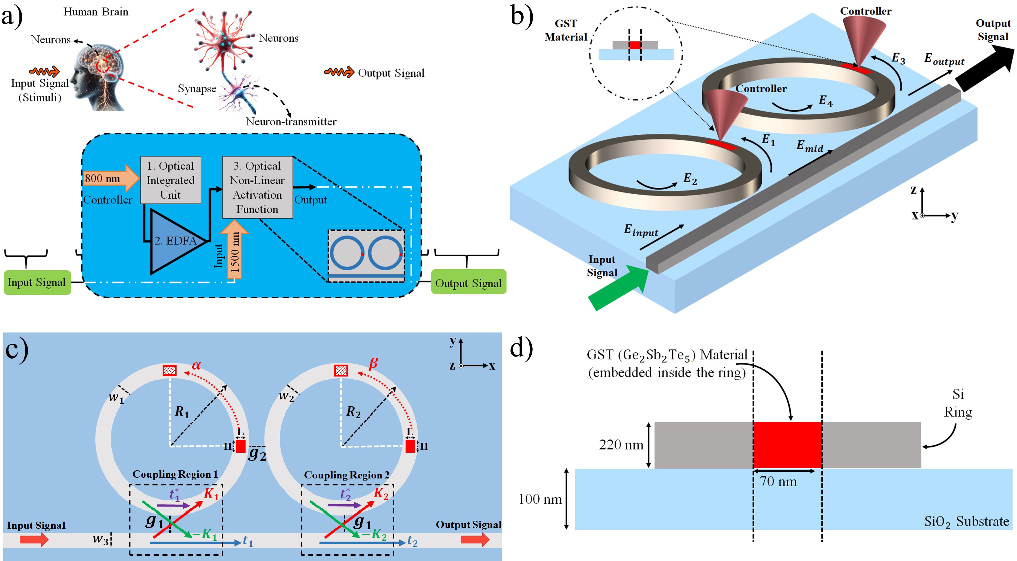
Our neuromorphic photonic device implements a nonlinear activation function through a novel double micro-ring resonator architecture with embedded phase-change material. Fig. 1 illustrates the device’s design principles and demonstrates its structural analogy to biological neural processing. The device architecture consists of a Si-based rectangular waveguide coupled to two ring resonators with integrated (GST) segments, all fabricated on a substrate. The operational principle of our device closely mirrors biological neural signal processing (Fig. 1a). Similar to how visual stimuli trigger neural responses through the human eye, optical input signals in our device propagate through defined pathways to generate controlled outputs. The input light wave enters through the waveguide port and sequentially couples to the first and second ring resonators through precisely engineered coupling regions (Fig. 1b,c). The device’s key structural parameters have been optimized for efficient operation. The ring widths , , and waveguide width are precisely controlled at 410 nm, 400 nm, and 410 nm respectively. Both rings maintain an outer radius (, ) of 5000 nm, with coupling gaps (100 nm) between the rings and waveguide, and (400 nm) between the rings themselves. The embedded GST segments measure L = 70 nm in length and H = 500 nm in height, while the entire structure maintains a uniform thickness of 220 nm. A distinctive feature of our design is the angular positioning capability of the GST segments, denoted by angles and in the first and second rings respectively (Fig. 1c). This configuration enables precise control over the device’s optical response through positional adjustments of the phase-change material. The light coupling behavior between components is governed by coupling coefficients , (straight transmission) and , (point coupling) at each coupling region. Detailed equations for resonance conditions and other key parameters including Free Spectral Range (FSR), Full Width at Half Maximum (FWHM), and Quality Factor (Q) are provided in the Supplementary Material Section 1.
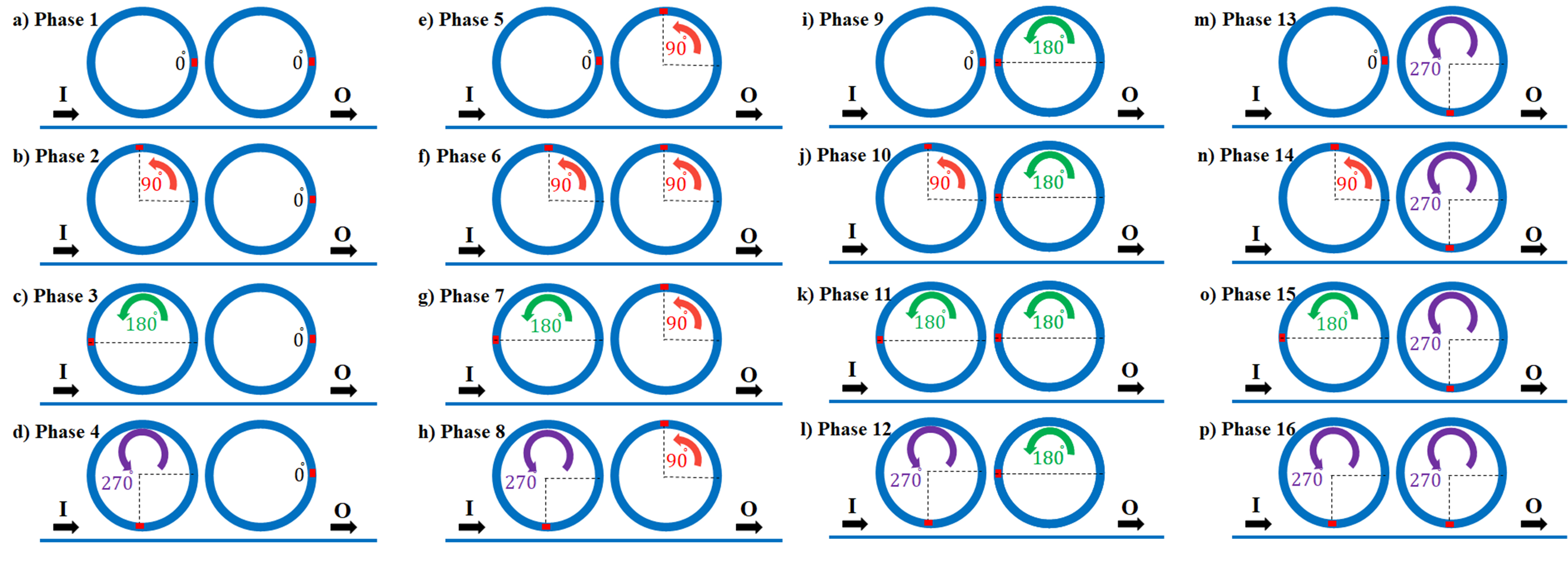
The tunability of our device was investigated through a systematic analysis of sixteen distinct GST material configurations, illustrated in Fig.2(a-p). These configurations explore the impact of varying angular positions of GST within both ring resonators on the device’s optical characteristics. The study encompasses four primary configuration sets, each demonstrating different combinations of angular shifts in the first and second rings. The first set (Fig. 2a-d) examines the effect of varying the GST position in the first ring from to while maintaining a fixed position in the second ring. In the second set (Fig. 2e-h), we introduce a shift in the second ring while maintaining the same angular variation pattern in the first ring. The third set (Fig. 2i-l) increases the second ring’s angular shift to , and the fourth set (Fig. 2m-p) extends this to , both while preserving the systematic variation in the first ring. Through comprehensive analysis of these configurations, based on criteria detailed in the Supplementary Material Section 3 (Table S1), we identified the seventh phase configuration (Fig. 2g) as optimal, exhibiting superior performance with minimal transmission coefficients. This optimal configuration features a GST material position in the first ring combined with a position in the second ring. Following this discovery, we conducted detailed investigations of the second ring’s width variations to further optimize the device’s performance.
Numerical calculations and results
We investigated the transmission characteristics of our device by calculating transmission coefficients for all sixteen phases at . The results, corresponding to the angular configurations shown in Fig. 2, demonstrate how GST’s phase-change properties can be leveraged to achieve precise optical switching control. Fig. 3(a-p) reveals how the transmission coefficient varies with GST material positioning inside the ring resonators. Each configuration exhibits two distinct resonant wavelengths, corresponding to the first and second rings - a key feature for implementing reliable nonlinear activation functions in neuromorphic computing. Our measurements reveal the following key findings: Initial Configuration (Phases 1-4, Fig. 3a-d): - Phase 1 shows resonant wavelengths at 1544.1 nm and 1547.37 nm, with transmission coefficients of 0.441 and 0.643 respectively, indicating minimal optical loss in the baseline configuration. With a angular shift in the first ring (Phase 3), the second resonant wavelength shifts to 1546.96 nm, yielding transmission coefficients of 0.0196 and 0.418. This dramatic change in transmission demonstrates the strong influence of GST positioning on light propagation within the rings. At shift (Phase 4), we observe transmission coefficients of 0.418 and 0.021, showing how angular positioning can be used to selectively suppress specific resonant modes Second Ring Configuration (Phases 5-8, Fig. 3e-h): - Resonant wavelengths stabilize at 1543.69 nm and 1546.96 nm, indicating a more consistent optical path length - Phase 6 ( shift in both rings) achieves low transmission coefficients of 0.011 and 0.0298, demonstrating enhanced optical switching capability. The optimal Phase 7 ( first ring, second ring) achieves near-zero and 0.0184 transmission coefficients, providing the sharp contrast needed for effective neuromorphic switching operations Advanced Configurations (Phases 9-16, Fig. 3i-p): - second ring shift (Phases 9-12) maintains resonant wavelengths while modulating transmission, showing the potential for reliable wavelength-selective switching - second ring shift (Phases 13-16) shows consistently near-zero transmission coefficients, suggesting complete optical isolation - a desirable feature for preventing crosstalk in integrated photonic circuits. A summary of all parameters obtained for sixteen different phases that represent the angular change of the GST material from angle to angle can be found in Supplementary Material Section S3. Also, this section includes the transmission coefficient calculated for all of the sixteen phases at and the results and summary table.
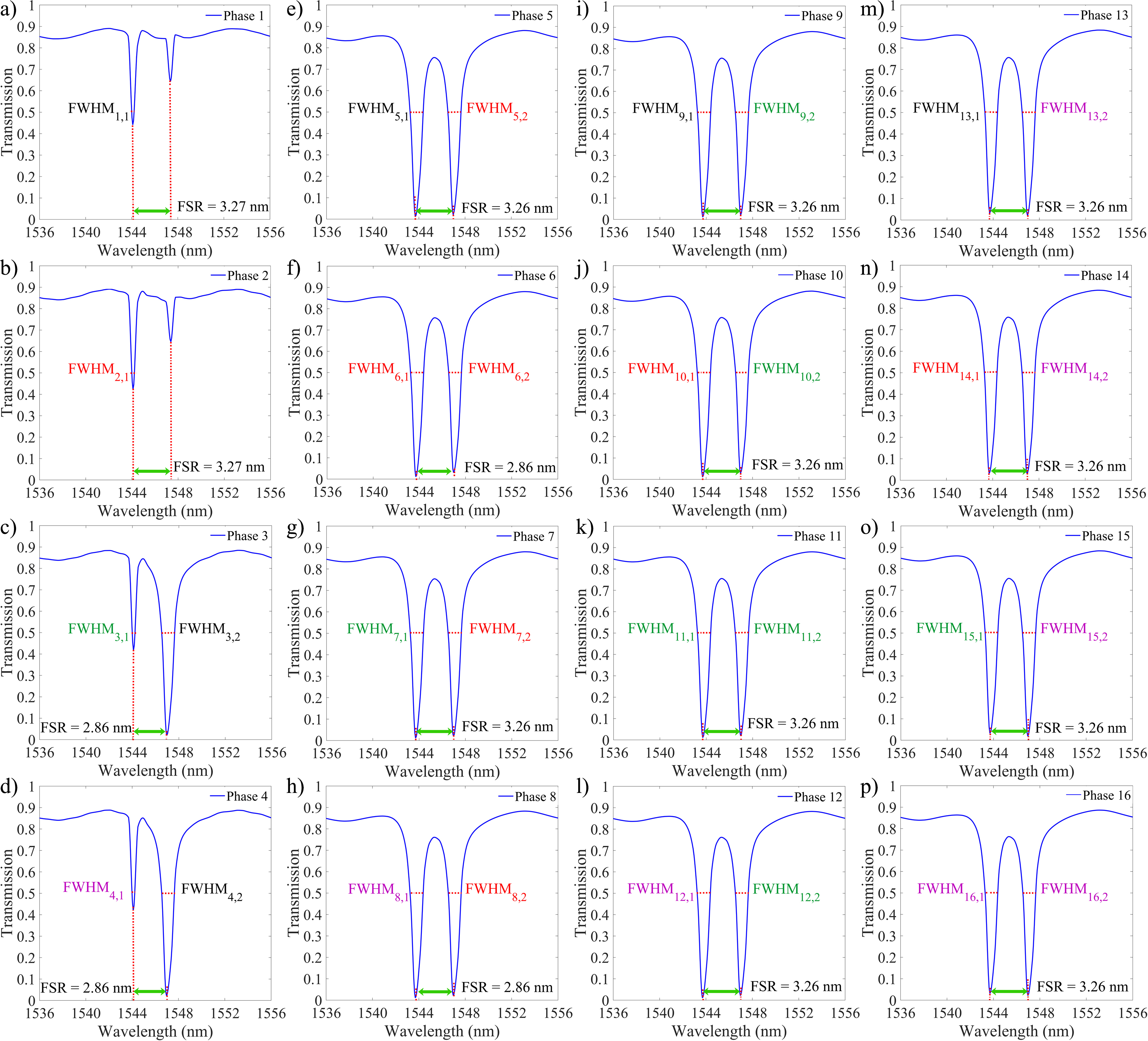
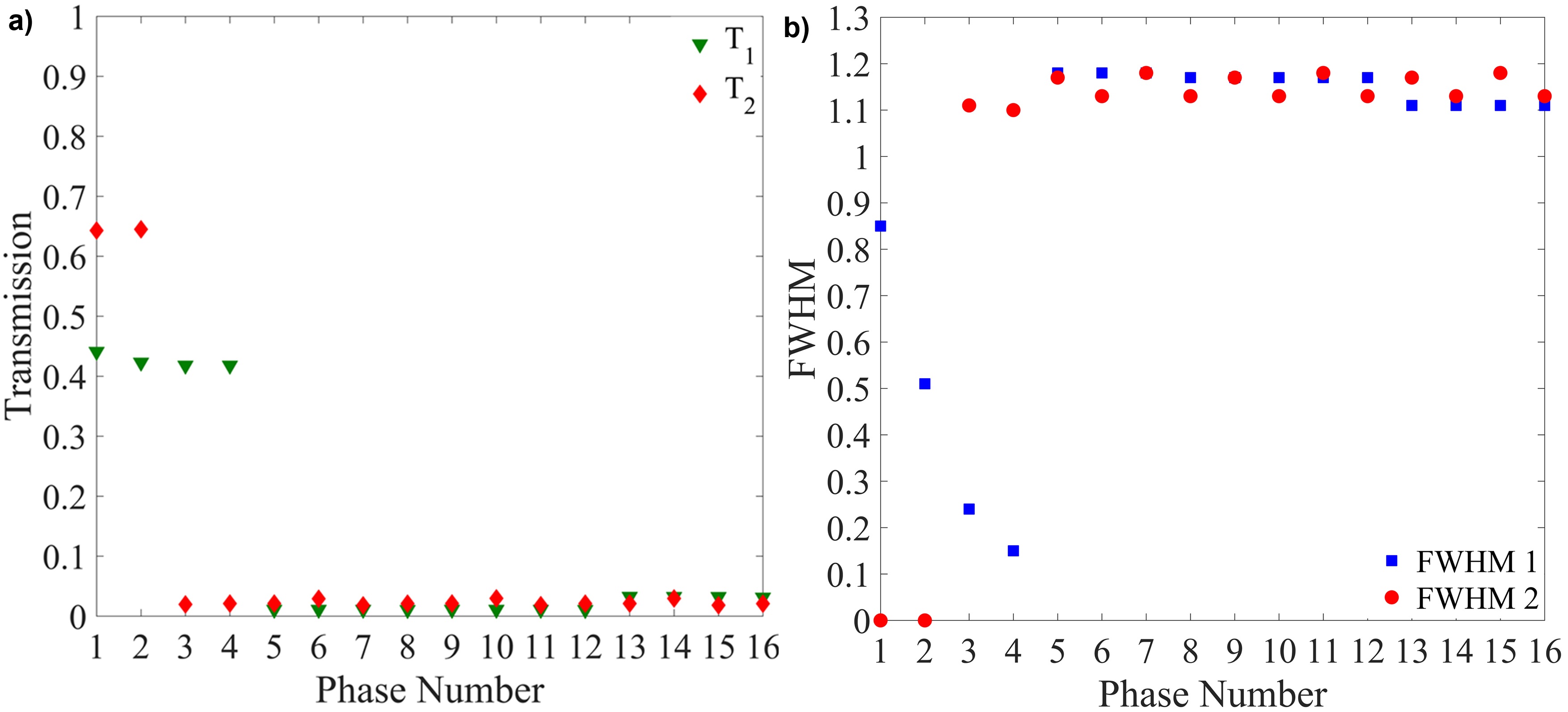
Fig. 4 reveals the critical relationship between transmission coefficients and spectral response in our GST-based ring resonator device. The transmission characteristics (Fig. 4a) demonstrate two distinct coefficients ( and ) representing light propagation through the first and second ring resonators, respectively. The steady decline in transmission coefficients across phase configurations (~0.4, ~0.65 in phases 1-4 dropping to near-zero in later phases) indicates increasingly effective optical mode confinement and GST-mediated absorption as the angular positions are optimized. The spectral characteristics, quantified by FWHM (Fig. 4b), expose a fundamental design trade-off inherent to ring resonator systems. Phases 1-4 achieve exceptionally narrow spectral widths ( ~0.2) due to strong resonant confinement, but their high transmission coefficients make them unsuitable for switching applications where high on-off contrast is essential. This behavior suggests that while these phases achieve excellent wavelength selectivity through constructive interference in the ring cavities, they fail to fully exploit GST’s phase-change properties for transmission modulation.
Notably, phases 7, 8, 11, and 12 strike an optimal balance between competing requirements. These configurations maintain consistent values around 1.1-1.2, indicating stable resonant behavior, while simultaneously achieving the low transmission coefficients necessary for effective switching. This performance sweet spot arises from the precise angular positioning of GST segments that maximizes light-matter interaction without compromising the resonant nature of the cavities. Temperature-dependent characterization at (detailed in Supplementary Material Section S3, Table S2) confirms phase seven as the ideal configuration. This phase maintains superior performance metrics across temperature variations, demonstrating robust switching behavior essential for practical neuromorphic computing applications. The resilience of phase seven to thermal variations suggests optimal alignment between the GST segments’ optical properties and the resonant modes of the coupled ring system. The transmission spectra for all 16 phase configurations, highlighting the effects of angular shifts in GST material within the rings, are detailed in Supplementary Material Section 3 (Figure S1).
Tolerance Analyzes
To optimize device performance and understand operational constraints, we conducted detailed investigations of structural and thermal parameters. Our analysis focused on two key aspects: dimensional variations in the ring resonators and temperature-dependent behavior of the GST material. We systematically investigated the impact of the second ring’s width variations on device performance, focusing on phase seven - our optimal configuration where GST materials in the first and second rings are positioned at and respectively (see Fig. 2). The width of the second ring was varied from 350 nm to 450 nm while maintaining other structural parameters: first ring width (410 nm), waveguide width (410 nm), ring radii and (both 5000 nm), coupling gaps (100 nm) and (400 nm), and GST segment dimensions L (70 nm) and H (500 nm). The thickness of the ring and the rectangular waveguide is 220 nm. Detailed transmission characteristics for these variations are provided in the Supplementary Material Section 4 (Table S3 and Figure S2).
The temperature-dependent behavior of our device reveals critical insights into its switching capabilities and operational stability. Fig. 5 demonstrates how temperature variation fundamentally alters the device’s transmission characteristics through GST’s phase-change properties. As temperature increases from to , the GST material undergoes significant changes in its optical properties, with its refractive index shifting from 3.25+0.09i to 5.6+0.85i [55]. Fig. 5a illustrates the evolution of transmission spectra across multiple temperatures ( to ), revealing distinct behavioral regimes. At room temperature (), the device exhibits a broad transmission peak centered around 1547.1 nm with a maximum coefficient of approximately 0.85. As temperature increases, we observe a systematic transformation of the transmission spectrum: - The primary transmission dip deepens and slightly blue-shifts - The spectral profile becomes more pronounced and asymmetric - Secondary features emerge at longer wavelengths The temperature-dependent transmission characteristics, summarized in Fig. 5b, demonstrate exceptional switching contrast. The transmission coefficient shows a dramatic modulation: - 0.643 at (initial state) - Drops to 0.00391 at (optimal switching point) - Partially recovers to 0.587 at - Stabilizes at 0.507 by This behavior suggests a complex interplay between GST’s phase transition and the resonant modes of our ring structure. The sharp transition observed corresponds to GST’s crystallization temperature, where the material undergoes significant changes in its optical properties. The subsequent partial recovery in transmission at higher temperatures indicates a refinement of the crystalline structure, offering additional degrees of control over the device’s optical response.
Fig. 6 reveals the temperature-dependent switching characteristics of phase seven, demonstrating enhanced performance compared to the baseline configuration. The spectral response (Fig. 6a) shows distinct temperature-dependent transmission features across the 1546-1553 nm wavelength range. At room temperature (), the device exhibits low transmission (0.0194) at 1547 nm, indicating strong optical confinement. As temperature increases to , we observe a dramatic shift in behavior with transmission peaking at 0.85 near 1551 nm, representing a remarkable 0.83 change in transmission coefficient across a 4 nm spectral window. The resonance wavelength shift from 1547.7 nm to 1550 nm across the range indicates controlled modification of the effective optical path length through GST’s thermo-optic response. Fig. 6b), shows that the transmission coefficient at is 0.0194 and increases to 0.376 while the temperature is and then decreases to 0.0.459 at , and finally increases to 0.435 at . The lower switching temperature () of phase seven not only improves energy efficiency but also enhances device longevity by operating well below GST’s crystallization temperature. The broader spectral response (4 nm) additionally provides more robust operation against thermal fluctuations and fabrication tolerances. The precise control over both spectral position and transmission amplitude demonstrates the potential for multi-level switching operations in neuromorphic computing applications.
The thermal behavior of our device, crucial for reliable switching operations, was characterized through detailed temporal and spatial analysis. Fig. 7 illustrates the cyclic temperature evolution during device operation, revealing precisely controlled thermal excursions between room temperature (Blue Line) and the operational maximum () - well below GST’s melting point of (Red Line). The temporal temperature evolution follows a modified exponential relationship[56].
| (1) |
Where is the initial temperature and here it is , is the temperature changes while the temperature increased from initial temperature to the peak value, which is called thermalization of the electrons and the lattice and it is . Also, is the cooling temperature amplitude (), , and are the heating and cooling rates, respectively. This asymmetric thermal response, with rapid heating and controlled cooling, enables efficient switching while preventing thermal degradation. The device demonstrates remarkable thermal cycling capability with a 0.5 ns cooling period, enabling switching rates up to 2 GHz. Each thermal cycle maintains precise control between the operational extremes, as evidenced by the consistent peak temperatures and baseline recovery shown in Fig. 7. The temperature-dependent transmission characteristics for all 16 GST phase configurations, including the significant changes in transmission coefficients between and , are detailed in Supplementary Material Figure S4 (Section 5).
The spatial heat distribution, visualized in Fig. 8, reveals distinct thermal profiles at operational extremes: - At Fig. 8a): Intense localized heating within the GST segments, with controlled thermal spreading ensuring sharp switching transitions - At (Fig. 8b): Minimal residual heating, confirming complete thermal recovery and system readiness for subsequent switching cycles This thermal characterization confirms our device’s capability for reliable high-speed switching while maintaining thermal stability - crucial requirements for neuromorphic computing applications.
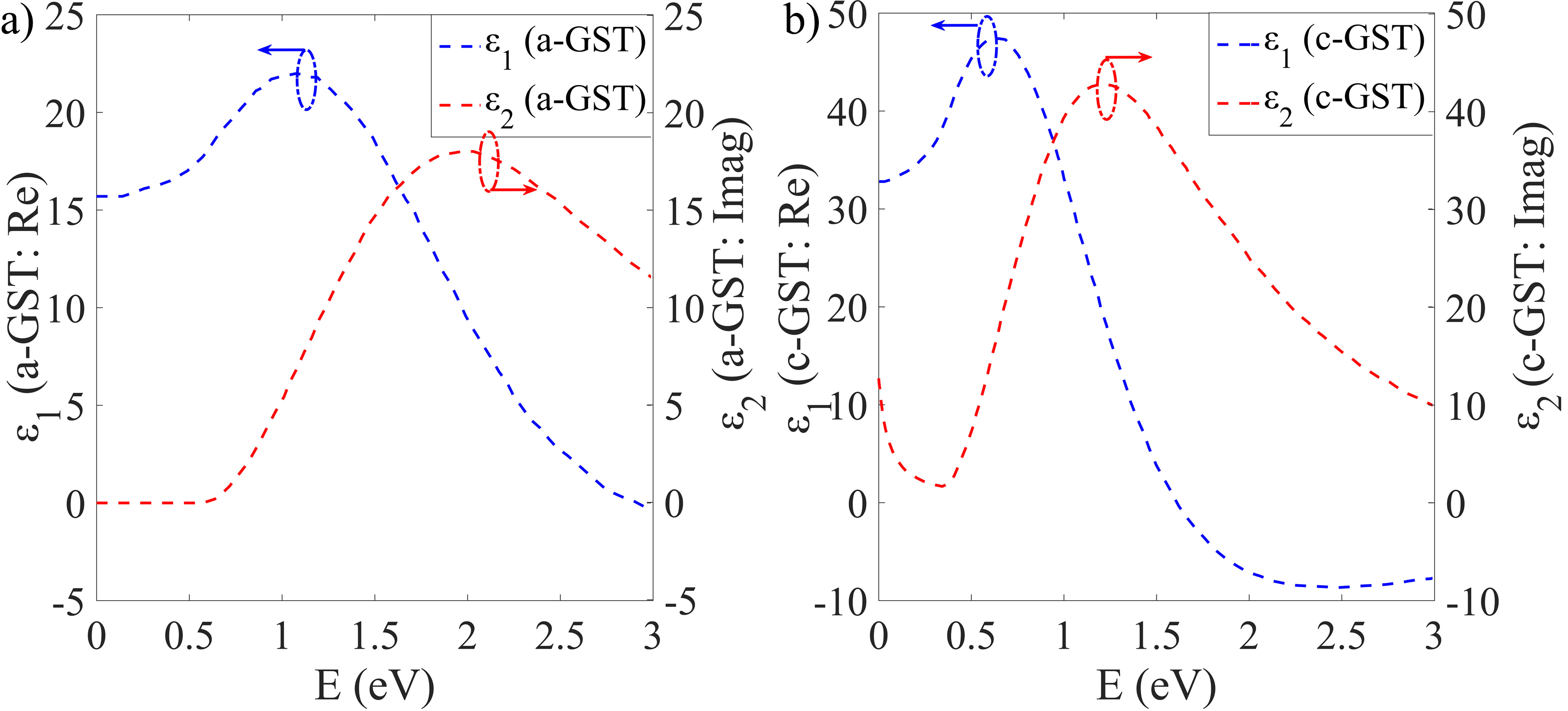
Fig. 9 reveals the fundamental optical properties of GST through its complex dielectric function () in both amorphous and crystalline states, providing insight into the material’s phase-dependent light-matter interactions. In the amorphous state (, Fig. 9a), we observe distinct behavior across different energy regimes: - Low-energy region (0-0.5 eV): The material exhibits minimal optical losses () with a positive real permittivity (), indicating dielectric behavior - Mid-energy region (0.5-1.5 eV): The imaginary component increases steadily while reaches its maximum (~22), suggesting enhanced light-matter interaction - High-energy region (>1.5 eV): decreases dramatically while maintains significant values, indicating strong optical absorption.
The crystalline state (, Fig. 9b) demonstrates markedly different characteristics: - Enhanced magnitude of both components ( peaks at ~48, reaches ~43) - Sharper transitions between energy regions - Notable transition to negative values above 1.5 eV, indicating metallic-like optical response. This phase-dependent evolution of dielectric properties enables our device’s switching functionality by providing significantly different optical responses at our operating wavelength (1550 nm 0.8 eV). The transition from positive to negative in the crystalline state is particularly significant when the energy exceeds from 1.5 eV, as it fundamentally alters the material’s interaction with incident light, enabling effective optical switching. The refractive index and dielectric function of GST material in both amorphous and crystalline states, critical for understanding the optical switching behavior, are analyzed in Supplementary Material Figures S6 and S7 (Section 7).
Discussion
Our work advances the field of neuromorphic computing by demonstrating how phase-change materials can be precisely engineered to emulate neural functionality at the hardware level. The developed GST-based double micro-ring resonator represents a fundamental building block for optical neural networks, offering several key advantages over traditional electronic implementations while more closely mimicking biological neural behavior.
The achievement of 0.5 ns switching speeds with our device architecture brings us closer to the temporal dynamics of biological neurons, while operating at significantly lower power due to the optical domain implementation. More importantly, the demonstrated ability to precisely control transmission characteristics through both thermal and geometric parameters provides a pathway for implementing complex neural functions. The combination of ultra-narrow band transmission (FWHM of 0.47 nm) and high switching contrast mirrors the all-or-nothing firing behavior of biological neurons, while the continuous tunability enables the weighted signal processing essential for neural computation.
A particularly significant finding is how the angular positioning of GST segments influences device characteristics. The optimal configuration (phase seven) achieves a delicate balance between switching contrast and spectral selectivity - analogous to how biological neurons maintain sensitivity while preventing spurious activation. This precise control over optical transmission, achieved through both material phase changes and geometric design, enables the implementation of nonlinear activation functions crucial for neural processing. The electric field distribution for Phase Seven, illustrating the field confinement at resonant wavelengths, is provided in Supplementary Material Figure S5 (Section 6).
The temperature-dependent operation of our device ( to ) demonstrates robust functionality well below GST’s melting point, suggesting practical feasibility for large-scale integration. The ability to achieve stable switching at relatively low temperatures () with rapid thermal cycling (2 GHz capability) addresses one of the key challenges in neuromorphic hardware: maintaining reliability while operating at speeds relevant to real-world applications.
Looking beyond individual device performance, our work has broader implications for neuromorphic computing:
1. The demonstrated integration of phase-change materials in photonic circuits provides a scalable approach for building dense neural networks. The double micro-ring architecture with precisely controlled GST angular positioning provides unprecedented control over switching characteristics while maintaining ultra-narrow band transmission (0.47 nm FWHM), enabling more precise neural activation functions than previous single-ring designs.
2. The achievement of multi-level switching capabilities through precise thermal control enables the implementation of synaptic plasticity. Our device achieves robust switching at lower operating temperatures () compared to conventional GST implementations (), while maintaining high contrast ratios - a critical advancement for practical neural network integration.
3. The combination of high switching speeds and spectral selectivity opens possibilities for wavelength-division multiplexing in neural networks. The distinctive combination of angular GST positioning and thermal control in our design enables independent optimization of spectral selectivity and switching contrast, offering new degrees of freedom for neural response tuning.
4. The low thermal budget and efficient switching behavior suggest potential for energy-efficient, large-scale neural systems. The demonstrated 0.5 ns cooling time with our optimized thermal management approach enables switching rates up to 2 GHz while maintaining stability well below GST’s melting point, addressing key speed-reliability trade-offs in neuromorphic systems
These capabilities, particularly the combination of precise spectral control and efficient thermal switching, establish a new approach to implementing optical neural functions that could overcome current limitations in scalability and energy efficiency. While existing photonic neuromorphic systems often sacrifice either switching speed or spectral selectivity, our design demonstrates that both can be simultaneously optimized through careful consideration of material positioning and thermal management.
The success of our GST-based double micro-ring resonator architecture opens exciting pathways for further development of neuromorphic photonic systems. Our demonstrated capabilities in precise thermal control and angular-dependent switching provide a robust foundation for advancing this technology. Building upon our validated switching approach, future work can extend these principles to implement additional neural functionalities, leveraging the demonstrated thermal stability and spectral precision. The proven design principles can be scaled to create larger networks that take full advantage of the achieved ultra-narrow band transmission characteristics. Our established thermal management techniques enable opportunities for coordinated operation of multiple resonator elements, while our high-speed optical switching capabilities can be integrated with existing control systems to maximize practical impact.
These directions leverage the fundamental advances demonstrated in our work - particularly the achievement of precise switching control through optimized GST positioning and thermal management - to advance the field of neuromorphic photonic computing. Our results establish a clear path forward for realizing practical, scalable optical neural networks, bringing us closer to the goal of efficient, brain-inspired computing architectures. This work represents a significant step toward realizing practical neuromorphic systems that can approach the efficiency and capability of biological neural networks. By demonstrating precise control over neural-like behavior in a photonic platform, we establish a promising direction for future brain-inspired computing architectures that could fundamentally transform how we process information.
Conclusion
We have demonstrated a novel approach to neuromorphic photonic computing through a GST-based double micro-ring resonator that achieves precise optical switching with unprecedented control over both spectral and thermal characteristics. By optimizing the angular positioning of GST segments within the ring resonators, we achieved ultra-narrow band transmission (FWHM of 0.47 nm) while maintaining high switching contrast - a combination that has proven challenging in previous implementations. The device operates efficiently at lower temperatures () than conventional GST-based systems, with switching speeds of 0.5 ns and thermal cycling capabilities up to 2 GHz. The key innovation lies in our dual-ring architecture’s ability to independently tune spectral selectivity and switching contrast through precise geometric and thermal control. This capability, combined with stable operation well below GST’s melting point and complete thermal recovery between switching cycles, addresses critical challenges in developing practical neuromorphic photonic devices. Our results establish that careful consideration of material positioning and thermal management can simultaneously optimize multiple performance metrics without the trade-offs typically encountered in photonic neuromorphic systems. This work not only advances the state of all-optical nonlinear activation functions but also provides a practical pathway toward scalable, energy-efficient neuromorphic computing architectures that more closely approximate biological neural processing..
Methods
Material Properties
The GST material can be used in both of the crystalline and amorphous states. The refractive index of the GST material can be changed from 3.25+0.09i to 5.6+0.85i. The refractive index of the GST material was taken from [57] and are available online in the Supplementary Material.
Fabrication Process
is a wafer layer, and 220 nm-thick layer of Si rectangular waveguide and ring resonators are placed on substrate layer with beam evaporation and lift-up process. Finally, ring resonators etched with exposing UV light and inserting nano-mask to embed GST layers inside the ring resonators. The length and width of the etching area is 70 nm and 500 nm, respectively. 220 nm-thick GST materials can be embedded with thermal evaporation inside the ring resonators.
Simulation
The finite element method is used to simulate the ring resonators with a structure of Si and GST material.
Data Availability
The data supporting the findings of this study are available within the article and its Supplementary Material. Additional detail data are available from the authors upon request. Raw data (Refractive index and dielectric function for the GST material) can be found online: https://github.com/HosseinKarimkhani/GST-Material-Raw-Data-Refractive-Index-Epsilon-/blob/main/CodeUpload.m
References
- [1] Jeong, D. S., Kim, K. M., Kim, S., Choi, B. J. & Hwang, C. S. Memristors for energy-efficient new computing paradigms. \JournalTitleAdvanced Electronic Materials 2, 1600090 (2016).
- [2] Teo, T. Y. et al. Programmable chalcogenide-based all-optical deep neural networks. \JournalTitleNanophotonics 11, 4073–4088 (2022).
- [3] Miscuglio, M., Adam, G. C., Kuzum, D. & Sorger, V. J. Roadmap on material-function mapping for photonic-electronic hybrid neural networks. \JournalTitleApl Materials 7 (2019).
- [4] Goi, E., Zhang, Q., Chen, X., Luan, H. & Gu, M. Perspective on photonic memristive neuromorphic computing. \JournalTitlePhotoniX 1, 1–26 (2020).
- [5] Shastri, B. J. et al. Neuromorphic photonics, principles of. \JournalTitleEncyclopedia of Complexity and Systems Science 1–37 (2018).
- [6] Fok, M. P., Tian, Y., Rosenbluth, D. & Prucnal, P. R. Asynchronous spiking photonic neuron for lightwave neuromorphic signal processing. \JournalTitleOptics letters 37, 3309–3311 (2012).
- [7] Hughes, T. W., Minkov, M., Shi, Y. & Fan, S. Training of photonic neural networks through in situ backpropagation and gradient measurement. \JournalTitleOptica 5, 864–871 (2018).
- [8] Siddique, R., Eftimie, M. & Banad, Y. M. A comparative analysis of neuromorphic neuron circuits for enhanced power efficiency and spiking frequency in 22nm cmos technology. In 2024 IEEE 67th International Midwest Symposium on Circuits and Systems (MWSCAS), 1096–1100 (IEEE, 2024).
- [9] Eslami, M. R., Biswas, D., Takhtardeshir, S., Sharif, S. S. & Banad, Y. M. On-chip learning with memristor-based neural networks: Assessing accuracy and efficiency under device variations, conductance errors, and input noise. \JournalTitlearXiv preprint arXiv:2408.14680 (2024).
- [10] Xu, B. et al. Recent progress of neuromorphic computing based on silicon photonics: Electronic–photonic co-design, device, and architecture. In Photonics, vol. 9, 698 (MDPI, 2022).
- [11] Xiang, S., Zhang, Y., Guo, X., Wen, A. & Hao, Y. Photonic generation of neuron-like dynamics using vcsels subject to double polarized optical injection. \JournalTitleJournal of Lightwave Technology 36, 4227–4234 (2018).
- [12] Antonik, P., Marsal, N., Brunner, D. & Rontani, D. Human action recognition with a large-scale brain-inspired photonic computer. \JournalTitleNature Machine Intelligence 1, 530–537 (2019).
- [13] Pedretti, G. et al. Memristive neural network for on-line learning and tracking with brain-inspired spike timing dependent plasticity. \JournalTitleScientific reports 7, 5288 (2017).
- [14] Fu, Z. et al. Programmable low-power consumption all-optical nonlinear activation functions using a micro-ring resonator with phase-change materials. \JournalTitleOptics Express 30, 44943–44953 (2022).
- [15] Xu, X. et al. Photonic perceptron based on a kerr microcomb for high-speed, scalable, optical neural networks. \JournalTitleLaser & Photonics Reviews 14, 2000070 (2020).
- [16] Zhou, H. et al. Photonic matrix multiplication lights up photonic accelerator and beyond. \JournalTitleLight: Science & Applications 11, 30 (2022).
- [17] Shastri, B. J. et al. Photonics for artificial intelligence and neuromorphic computing. \JournalTitleNature Photonics 15, 102–114 (2021).
- [18] Shen, B. et al. Integrated turnkey soliton microcombs. \JournalTitleNature 582, 365–369 (2020).
- [19] Xu, X. et al. 11 tops photonic convolutional accelerator for optical neural networks. \JournalTitleNature 589, 44–51 (2021).
- [20] Dupuis, N. et al. Nanosecond-scale mach–zehnder-based cmos photonic switch fabrics. \JournalTitleJournal of Lightwave Technology 35, 615–623 (2016).
- [21] Zheng, J. et al. Gst-on-silicon hybrid nanophotonic integrated circuits: a non-volatile quasi-continuously reprogrammable platform. \JournalTitleOptical Materials Express 8, 1551–1561 (2018).
- [22] Zhang, Q., Yu, H., Barbiero, M., Wang, B. & Gu, M. Artificial neural networks enabled by nanophotonics. \JournalTitleLight: Science & Applications 8, 42 (2019).
- [23] Nahmias, M. A., Shastri, B. J., Tait, A. N., De Lima, T. F. & Prucnal, P. R. Neuromorphic photonics. \JournalTitleOptics and Photonics News 29, 34–41 (2018).
- [24] Ferreira de Lima, T., Shastri, B. J., Tait, A. N., Nahmias, M. A. & Prucnal, P. R. Progress in neuromorphic photonics. \JournalTitleNanophotonics 6, 577–599 (2017).
- [25] Chen, Z. et al. Deep learning with coherent vcsel neural networks. \JournalTitleNature Photonics 17, 723–730 (2023).
- [26] Diehl, P. U. et al. Fast-classifying, high-accuracy spiking deep networks through weight and threshold balancing. In 2015 International joint conference on neural networks (IJCNN), 1–8 (ieee, 2015).
- [27] Zhang, H. et al. An optical neural chip for implementing complex-valued neural network. \JournalTitleNature communications 12, 457 (2021).
- [28] Chakraborty, I., Saha, G., Sengupta, A. & Roy, K. Toward fast neural computing using all-photonic phase change spiking neurons. \JournalTitleScientific reports 8, 12980 (2018).
- [29] Li, T. et al. Neuromorphic photonics based on phase change materials. \JournalTitleNanomaterials 13, 1756 (2023).
- [30] AbouHassan, I., Kasabov, N. K., Jagtap, V. & Kulkarni, P. Spiking neural networks for predictive and explainable modelling of multimodal streaming data with a case study on financial time series and online news. \JournalTitleScientific Reports 13, 18367 (2023).
- [31] Shiflett, K., Wright, D., Karanth, A. & Louri, A. Pixel: Photonic neural network accelerator. In 2020 IEEE International Symposium on High Performance Computer Architecture (HPCA), 474–487 (IEEE, 2020).
- [32] Feldmann, J., Youngblood, N., Wright, C. D., Bhaskaran, H. & Pernice, W. H. All-optical spiking neurosynaptic networks with self-learning capabilities. \JournalTitleNature 569, 208–214 (2019).
- [33] Ovshinsky, S. R. Reversible electrical switching phenomena in disordered structures. \JournalTitlePhysical review letters 21, 1450 (1968).
- [34] Abdollahramezani, S. et al. Tunable nanophotonics enabled by chalcogenide phase-change materials. \JournalTitleNanophotonics 9, 1189–1241 (2020).
- [35] Meinders, E. R., Mijiritskii, A. V., van Pieterson, L. & Wuttig, M. Optical data storage: Phase-change media and recording, vol. 4 (Springer Science & Business Media, 2006).
- [36] Yamada, N. et al. High speed overwritable phase change optical disk material. \JournalTitleJapanese Journal of Applied Physics 26, 61 (1987).
- [37] Stegmaier, M., Ríos, C., Bhaskaran, H., Wright, C. D. & Pernice, W. H. Nonvolatile all-optical 1 2 switch for chipscale photonic networks. \JournalTitleAdvanced Optical Materials 5, 1600346 (2017).
- [38] Wuttig, M., Bhaskaran, H. & Taubner, T. Phase-change materials for non-volatile photonic applications. \JournalTitleNature photonics 11, 465–476 (2017).
- [39] Cheng, Z., Ríos, C., Pernice, W. H., Wright, C. D. & Bhaskaran, H. On-chip photonic synapse. \JournalTitleScience advances 3, e1700160 (2017).
- [40] Ríos, C. et al. Integrated all-photonic non-volatile multi-level memory. \JournalTitleNature photonics 9, 725–732 (2015).
- [41] Yu, T. et al. All-chalcogenide programmable all-optical deep neural networks. \JournalTitlearXiv preprint arXiv:2102.10398 (2021).
- [42] Liu, B. et al. Universal memory based on phase-change materials: From phase-change random access memory to optoelectronic hybrid storage. \JournalTitleChinese Physics B 30, 058504 (2021).
- [43] Rasmussen, T. S., Yu, Y. & Mork, J. All-optical non-linear activation function for neuromorphic photonic computing using semiconductor fano lasers. \JournalTitleOptics Letters 45, 3844–3847 (2020).
- [44] Psaltis, D. & Farhat, N. Optical information processing based on an associative-memory model of neural nets with thresholding and feedback. \JournalTitleOptics Letters 10, 98–100 (1985).
- [45] Jutamulia, S. & Yu, F. Overview of hybrid optical neural networks. \JournalTitleOptics & Laser Technology 28, 59–72 (1996).
- [46] Rosenbluth, D., Kravtsov, K., Fok, M. P. & Prucnal, P. R. A high performance photonic pulse processing device. \JournalTitleOptics express 17, 22767–22772 (2009).
- [47] Gholipour, B. et al. Amorphous metal-sulphide microfibers enable photonic synapses for brain-like computing. \JournalTitleAdvanced Optical Materials 3, 635–641 (2015).
- [48] Luo, L. Principles of neurobiology (Garland Science, 2020).
- [49] Karimkhani, H., Attariabad, A. & Vahed, H. High sensitive plasmonic sensor with simple design of the ring and the disk resonators. \JournalTitleOptical and Quantum Electronics 54, 344 (2022).
- [50] Zhang, W. et al. Harnessing plasma absorption in silicon mos ring modulators. \JournalTitleNature Photonics 17, 273–279 (2023).
- [51] Aghdasinia, S., Allahverdizadeh, H., Afkari, E., Ahmadpour, B. & Bemani, M. Optimizing an electromagnetic wave absorber for bi-anisotropic metasurfaces based on toroidal modes. \JournalTitleScientific Reports 14, 8783 (2024).
- [52] Sharif, S. S., Karimkhani, H. & Banad, Y. M. Exploring nonlinear activation function within microring resonators for all-photonic neuromorphic computing. In Physics and Simulation of Optoelectronic Devices XXXII, vol. 12880, 189–193 (SPIE, 2024).
- [53] Banad, Y. M., Hasan, S. M. A., Sharif, S. S., Veronis, G. & Gartia, M. R. Optical properties and behavior of whispering gallery mode resonators in complex microsphere configurations: Insights for sensing and information processing applications. \JournalTitleNano Select 5, 2300184 (2024).
- [54] Cai, L., Lu, Y. & Zhu, H. Performance enhancement of on-chip optical switch and memory using ge2sb2te5 slot-assisted microring resonator. \JournalTitleOptics and Lasers in Engineering 162, 107436 (2023).
- [55] Xu, Z. et al. Optical constants acquisition and phase change properties of ge 2 sb 2 te 5 thin films based on spectroscopy. \JournalTitleRSC advances 8, 21040–21046 (2018).
- [56] Waldecker, L. et al. Time-domain separation of optical properties from structural transitions in resonantly bonded materials. \JournalTitleNature materials 14, 991–995 (2015).
- [57] Kim, H. J., Sohn, J.-w., Hong, N., Williams, C. & Humphreys, W. Pcm-net: a refractive index database of chalcogenide phase change materials for tunable nanophotonic device modelling. \JournalTitleJournal of Physics: Photonics 3, 024008 (2021).
Author contributions statement
Must include all authors, identified by initials, for example: A.A. conceived the experiment(s), A.A. and B.A. conducted the experiment(s), C.A. and D.A. analysed the results. All authors reviewed the manuscript.
Additional information
Supplementary information accompanies this paper at.
Raw data (Refractive index and dielectric function for the GST material) can be found online: GST-Material-Raw-Data-Refractive-Index-Epsilon
The corresponding author is responsible for submitting a competing interests statement on behalf of all authors of the paper. This statement must be included in the submitted article file.