Inverse Rashba-Edelstein THz emission modulation induced by ferroelectricity in CoFeB/PtSe2/MoSe2//LiNbO3 systems
Abstract
Spintronic Terahertz emitters, based on optically triggered spin-to-charge interconversion processes, have recently emerged as novel route towards compact and efficient THz sources. Yet, the next challenge for further technologically-relevant devices remains to modulate the emission, with low-energy consumption operation. To this aim, ferroelectric materials coupled to active spin-orbit layers such as two-dimensional transition metal dichalcogenides are suitable candidates. In this work, we present the realization of a large area heterostructure of CoFeB/PtSe2/MoSe2 on a bi-domain LiNbO3 substrate. Using THz time-domain spectroscopy, we show that the ferroelectric polarization direction induces a sizeable modulation of the THz emission. We rationalise these experimental results by using band structure and spin accumulation calculations that are consistent with an interfacial spin-to-charge conversion mediated by inverse Rashba-Edelstein effect at the MoSe2/PtSe2 interface and being tuned by ferroelectricity in the adjacent LiNbO3 surface. This work points out the relevance of field effect spin-orbit architectures for novel THz technologies.
Introduction
Over the last decade, huge efforts have been put forward in the development of novel kind of THz sources based on ultrafast spin-to-charge interconversion, thus referred as spintronic THz emitters. These emitters are defined, in their simplest form, by a heterostructure made of nanometer thick ferromagnetic (FM)/non-magnetic (NM) junctions. When excited by an ultrashort optical pulse, an out-of-equilibrium spin current is generated in the FM layer that is diffused and converted to a transient charge current on the NM side. This layer acts as an active spin-orbit layer and subsequently leads to the generation of a linearly polarized THz pulse [1]. The spin-to-charge conversion (SCC) is driven by the inverse spin-Hall effect in the case of bulk spin-orbit materials like heavy metals [2], and/or mediated by the inverse Rashba-Edelstein effect (IREE) at the FM/NM interface in the presence of a spin-polarized texture [3, 4], e.g. on the surface of topological insulators [5, 6, 7].
Such ultrathin emitters exhibit broadband and gap-less THz emission spectrum over a few tens of THz, and their polarization direction can be easily controlled by a small applied magnetic field oriented in the sample plane. Many works have been subsequently carried out in order to increase the absolute emitter power by optimizing multisequenced stacks, thicknesses and the nature of FM and NM in the heterostructure [8, 9]. This progress has led to optimized emitters with performance already surpassing usual THz sources such as non-linear crystals [10], making spintronic emitters concrete candidates for the development of THz technologies. In particular, the THz spectral band is expected to be of paramount importance in the development of the next generation telecommunication standard [11], with various applications such as high speed wireless communication, nano-networks and networks-on-a-chip. However, these applications require controlling the emission with an external degree of freedom in order to encode information. Due to the recent emergence of spintronic emitters, only a few works have addressed this crucial need towards different strategies like patterning the emitter itself or using complex optical excitation schemes [12, 13]. Nevertheless, such methods remain limited as they permanently affect the design of the emitter or require bulky and energy-consuming equipments, thus reducing device scalability and adaptability.
Another relevant approach relies on the combination of ferroelectric materials with 2D electron gas, such as one made of an ultrathin 2D material with strong spin-orbit coupling [14]. These field effect spin-orbit (FESO) devices allow to control the spin-orbit coupling in the 2D layer via ferroelectricity, which could be switched externally by the application of a gate voltage [15]. It is thus particularly appealing for the development of low-consumption THz devices to couple such non-volatile voltage-controlled switching with a source of spin-current, in order to generate and modulate THz emission.
The key ingredients for this aim are therefore (i) a stabilized and technologically relevant ferroelectric material (ii) a suitable 2D material with spin textures modulated by electric field, which could be easily grown or transferred onto the ferroelectric material and (iii) an entire heterostructure with a mm-sized active surface for an easy activation by optical pulses.
On one hand, lithium niobate (LiNbO3) is a well known ferroelectric material, hosting a polarization pointing along the c-axis of the hexagonal unit cell. Owing to its THz emission properties [16, 17], it has been extensively studied at THz frequencies, and is widely used in optoelectronic devices for telecommunication, allowing high modulation speed up to several tens of GHz in the C-band [18]. On the other hand, ultrathin layers of transition metal dichalcogenide (TMD) such as PtSe2 possess several advantages to tackle the aforementioned (ii) requirement. The electronic and optical properties of such van der Walls (vdW) heterostructures can be tuned by the number of stacked layers [19], they possess strong spin-orbit coupling and their band structure can be strongly modified in contact with a ferroelectric material [20]. Additionally, single crystal PtSe2 of controlled thickness can be grown by molecular beam epitaxy (MBE) over waver-scale dimensions, in contrast with exfoliated layers. Yet, a direct growth of high quality TMD layers over large ferroelectric substrates remains challenging in terms of chemical compatibilities, and secondly as growth temperature conditions may alter ferroelectricity.
In this work, we present the realization of a field effect spin-orbit structure made of CoFeB/PtSe2/MoSe2 on a bi-domain LiNbO3 substrate, allowing to modulate THz emission via ferroelectricity while excited by ultrashort optical pulses. The samples were prepared by transferring high quality MBE-grown TMD layers on a single LiNbO3 wafer with cm-scale out-of-plane pre-poled areas in opposite directions. Using THz time-domain spectroscopy, we first show that the poled areas can be clearly identified in the non-magnetic THz signature, and that the ferroelectric polarization direction leads to a sizeable modulation of the magnetic THz emission. We then interpret this result by a spin-to-charge conversion mediated by IREE, with the existence of ferroelectrically-controlled Rashba states at the PtSe2/MoSe2 interface. Using Density Functional Theory calculations, we finally demonstrate that the ferroelectricity direction shifts accordingly the TMD bands, thus supporting our experimental results and subsequent analysis.
I Fabrication and characterization.
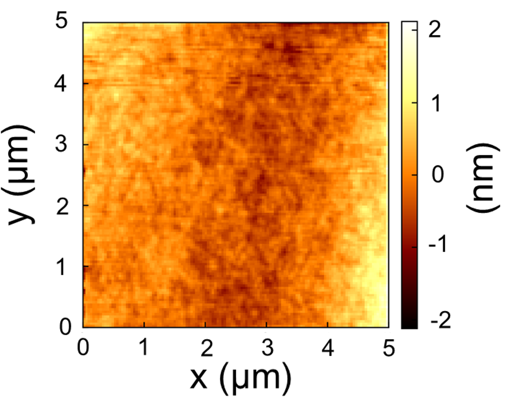
Samples were first prepared from a LiNbO3 wafer provided by Covesion, with pre-poled out-of-plane polarization areas along opposite directions. The wafer was cut into 10x10 mm² coupons, with half the area hosting a polarization towards the surface (up area) and half towards its back (down area). As depicted in Fig. 1a-b, piezoresponse force microscopy characterization confirms the existence of well-defined up and down polarization areas over a large scale, with a very low roughness surface (RMS=0.33 nm, see Suppl. Info. A).
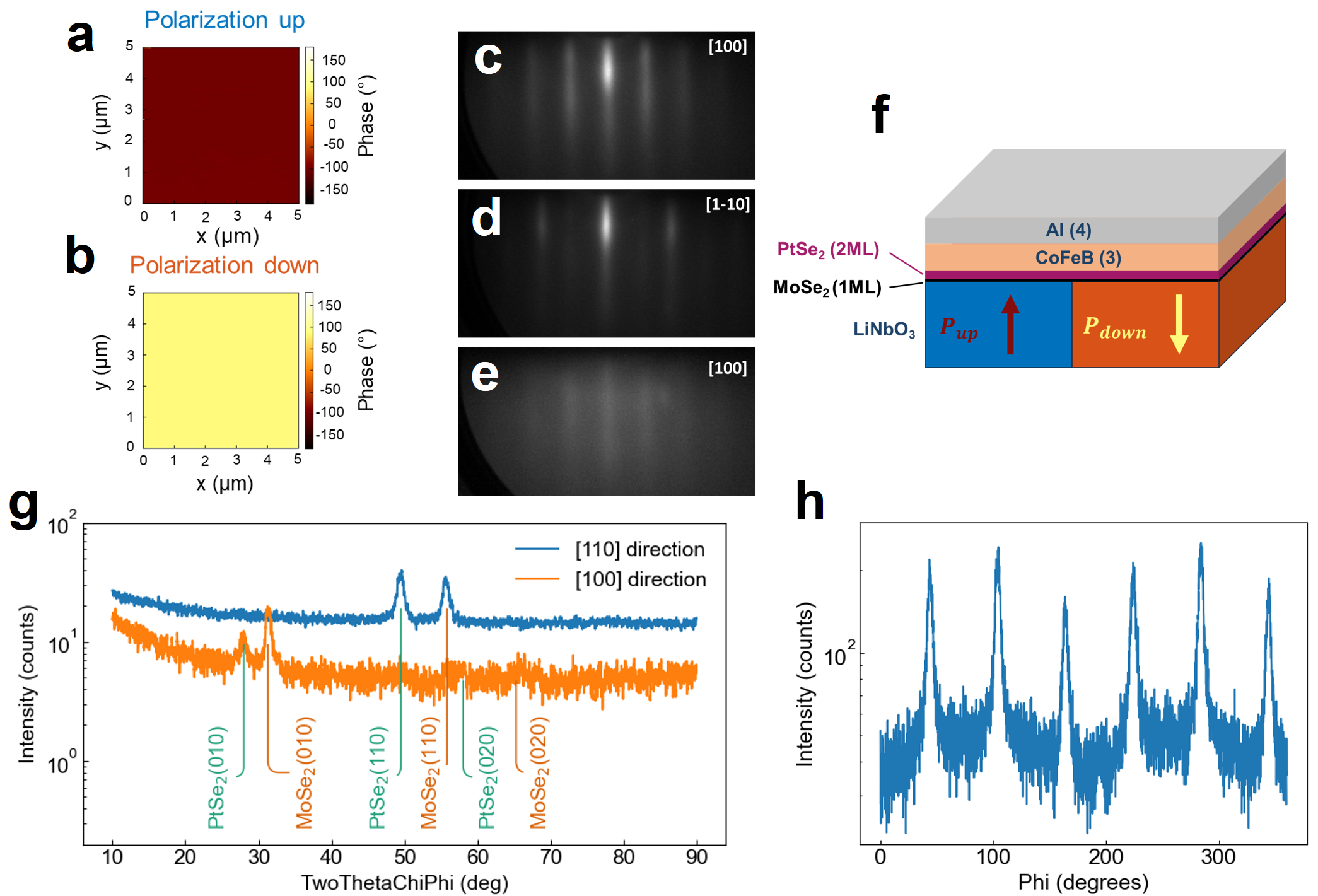
The 2D layers constituting the MoSe2/PtSe2 vdW heterostructure were grown using molecular beam epitaxy. Molybdenum and Platinum were evaporated with a rastered electron beam and directed onto a Mica substrate under Selenium flux. A calibrated quartz crystal balance was used to accurately measure the layer thickness such that 1 monolayer (1ML) of MoSe2 could be grown, followed by 2 monolayers (2ML) of PtSe2, and the quality of the growth was monitored in-situ with reflected high-energy electron diffraction (RHEED). Fig. 1c shows the RHEED pattern along the [100] direction directly after growth, with clear diffraction rods indicating true 2-dimensional growth of the TMD layers. The complementary diffraction pattern in Fig. 1d indicates anisotropy in the diffracted signal and is testament to the single crystal nature of the 2-dimensional growth by MBE. The process to delaminate the 2D material in an aqueous environment that allows for cm-scale layers to be transferred from one substrate to another, has been outlined elsewhere [21, 20]. This procedure was carried out to transfer the PtSe2(2 ML)/MoSe2(1 ML) heterostructure onto the LiNbO3 substrate, thus ensuring the same fabrication conditions for up and down areas. The sample is followingly annealed by slowly ramping up to around 250°C in increments and held there for around an hour before cooling down, allowing to improve the surface flatness between LiNbO3 and the 2D layers while preventing alteration of the ferroelectric substrate. Finally, a 3 nm-thick ferromagnetic layer made of CoFeB is deposited by sputtering without breaking vacuum, followed by 4 nm of Al to prevent oxidation, defining the heterostructure depicted in Fig. 1f. We confirm that the full stack is preserved after the transfer by in-plane X-ray diffraction measurements, which show the main characteristic diffraction peaks for each layers (Fig. 1g). An azimuthal scan of the PtSe2 [110] diffraction peak (Fig. 1h), showing a clear six-fold symmetry, finally confirms that crystallinity is preserved after the transfer process.
II THz-time domain spectroscopy characterization.
We now turn to the optical characterization of our sample, using standard THz time-domain spectroscopy technique in transmission mode. The heterostructure is excited from the substrate side (LiNbO3) at normal incidence by linearly polarized 80 fs-long pulses centered at 800 nm, delivered by a Yb-doped solid state femtosecond laser coupled to an optical parametric amplifier, while applying a small in-plane magnetic field (20mT). The repetition rate is 150 kHz and the beam waist on the sample is 250 µm. The emitted THz pulses are then detected orthogonally to the magnetic field by electro-optic sampling [22] with a 200 µm-thick ZnTe crystal, using the main output of the oscillator (130 fs pulses centered at 1030 nm).
Note that there are two possible sources of THz radiation within the heterostructure, each relying on different mechanisms. Under near infrared ultrafast excitation, the ferroelectric layer leads to THz emission via optical rectification, whereas the ultrafast demagnetization of the CoFeB is expected to generate THz via SCC. Pumping the sample through its substrate and detecting the emission in transmission geometry thus avoids the THz signature originating from SCC to be altered by LiNbO3 absorption at THz frequencies [23].
In order to extract the underlying symmetries of the system, we probe up and down ferroelectric areas while rotating the sample along its azimuthal axis, for two opposite directions of the magnetic field (i.e. setting the magnetization of CoFeB layer in the direction of the field). Such measurements allow to extract the non-magnetic and magnetic contributions to the THz emission by performing the sum and difference of the time traces, respectively [24].
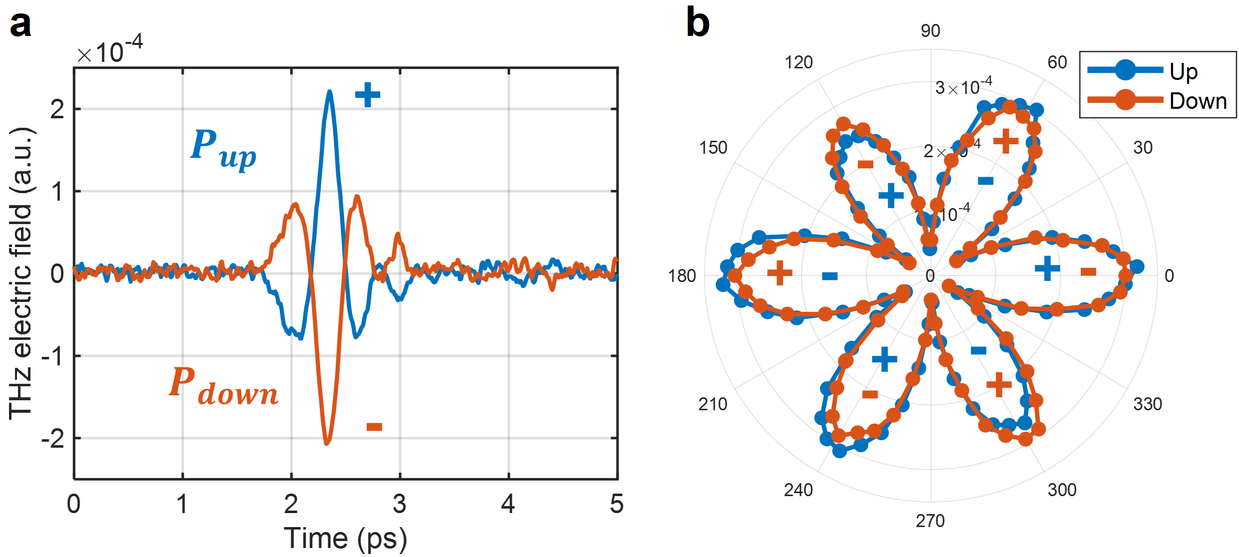
We first focus on the non-magnetic contribution to the THz emission. In Fig. 2a, the measured THz time trace is exhibiting a full phase reversal by switching between up and down ferroelectric areas. As the non-magnetic part originates from a non-linear second order effect ( of LiNbO3) [25], reversing the ferroelectric polarization is equivalent to flip the sample, i.e. inverting the dielectric tensor, thus reversing the phase of THz emission. This property is also preserved for any azimuthal angle, as depicted in Fig. 2b. While rotating the sample and reporting the peak-to-peak THz amplitude on a polar plot, we recover a three-fold symmetry for both pre-poled areas, characteristic of optical rectification in Z-cut LiNbO3 crystals, with reversed phase in each lobe. Thanks to this observation, we can clearly identify the ferroelectric state of the probed area.
We now move to the magnetic part of the THz emission. The measured temporal THz profiles obtained from the excitation of up and down ferroelectric areas are displayed in Fig. 3a. The two time traces have the same positive phase, and we observe a sizable increase of the THz emission in the up-poled area compared to the down one. This result shows that the ultrafast spin current generated in the FM layer under illumination is efficiently converted into a charge current into adjacent layers, in the vicinity of LiNbO3/2D interface. Note that in that case, the SCC process is isotropic as expected [6, 24, 19]. The influence of incident power is then investigated to further characterize the magnetic emission process, as depicted in Fig. 3b. The power dependence shows a typical behavior for SCC, linear at low power and starting to saturate above 80 mW. Interestingly, the magnetic THz contribution remains always higher for the up area over the entire power range, corroborating the influence of ferroelectricity direction on SCC efficiency. We evaluate the induced ferroelectric modulation on SCC to be about 15-20 (see top of Fig. 3b).
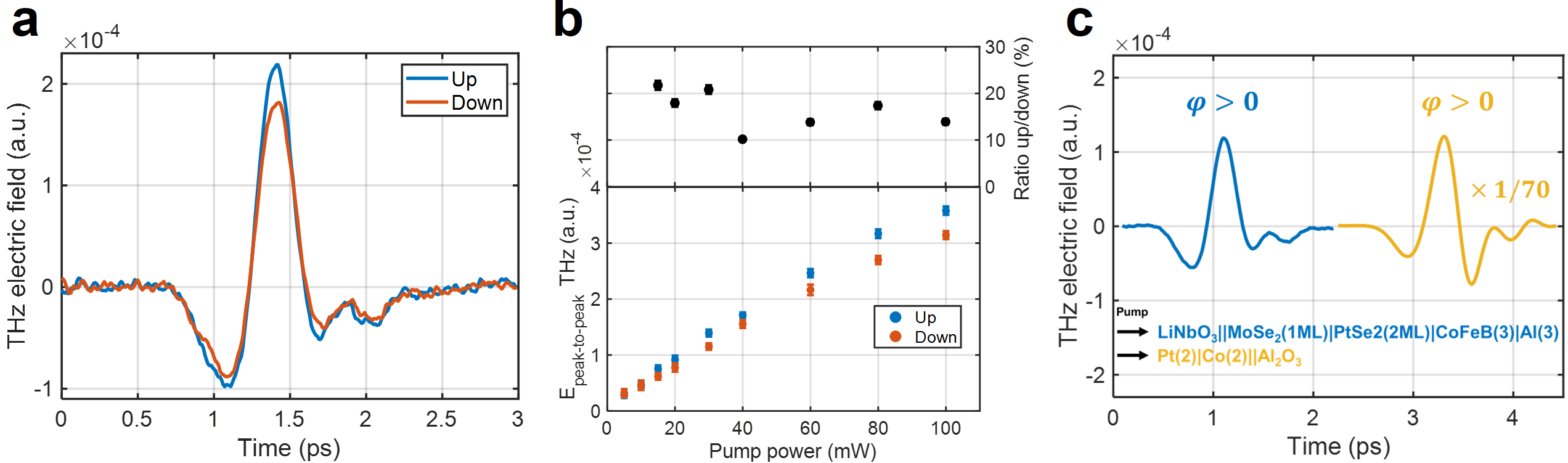
In order to gain more insight into the source of SCC, the THz emission amplitude and phase of our stack are further compared to a standard spintronic THz emitter made of Pt/Co grown on a sapphire substrate (Fig. 3c). Since the conversion occurs in the proximity of LiNbO3/2D interface - which is further supported by our calculations shown afterwards - both samples are probed while keeping the same stacking order between spin convertor (Pt for standard emitter) and spin injector (FM layer), with respect to incident optical excitation. We observe a positive phase for the two systems, and the amplitude is about 70 times larger for Pt/Co compared to our heterostructure. According to previous experimental reports on CoFeB/PtSe2 as a function of the TMD thickness [19], the THz magnetic emission is reduced by a factor 10 by reducing the number of TMD MLs from 10 to 2, transitioning from a SCC mediated by ISHE to IREE. Additionally, Pt and PtSe2 share the same conversion sign with a reduced emission by a factor 7 considering the same Pt thickness. Taking into account the sign and amplitude of THz emission, our results thus strongly indicate that the conversion mainly occurs in the vicinity of PtSe2 through IREE interfacial conversion.
III Density Functionnal Theory calculations.
We now turn to Density Functional Theory of SCC phenomena in these systems. The band structures, spin texture and SCC linear response (Rashba-Edelstein tensor) were calculated by a home-made procedure using the Hamiltonian and overlap matrices, based on methods and equations described in Suplementary Information B. Our first major results suggest that the SCC mainly occurs at the interface between MoSe2 and PtSe2, from states lying in a finite energy window of the valence band, as discussed in the following. In Fig. 4a, we first refer to the projected density of states on each layers forming the vdW heterostructure, extracted from the projected band structure (see Supl. Info. C). We recover the main feature of each layer, namely the presence of semi-conducting gap, together with an increase of MoSe2 density of states in an energy window between -2 and -1 eV (dashed red rectangle). The charge density map in the inset of Fig. 4a additionally highlights the conversion location in the heterostructure, showing a strong hybridization between MoSe2 and PtSe2 layers. Since MoSe2 takes part to the inversion symmetry breaking, it lifts the degeneracy present in PtSe2 leading to a Rashba effect as already reported in the case of PtSe2/Gr bilayers [19], in which SCC also occurs in the valence band.
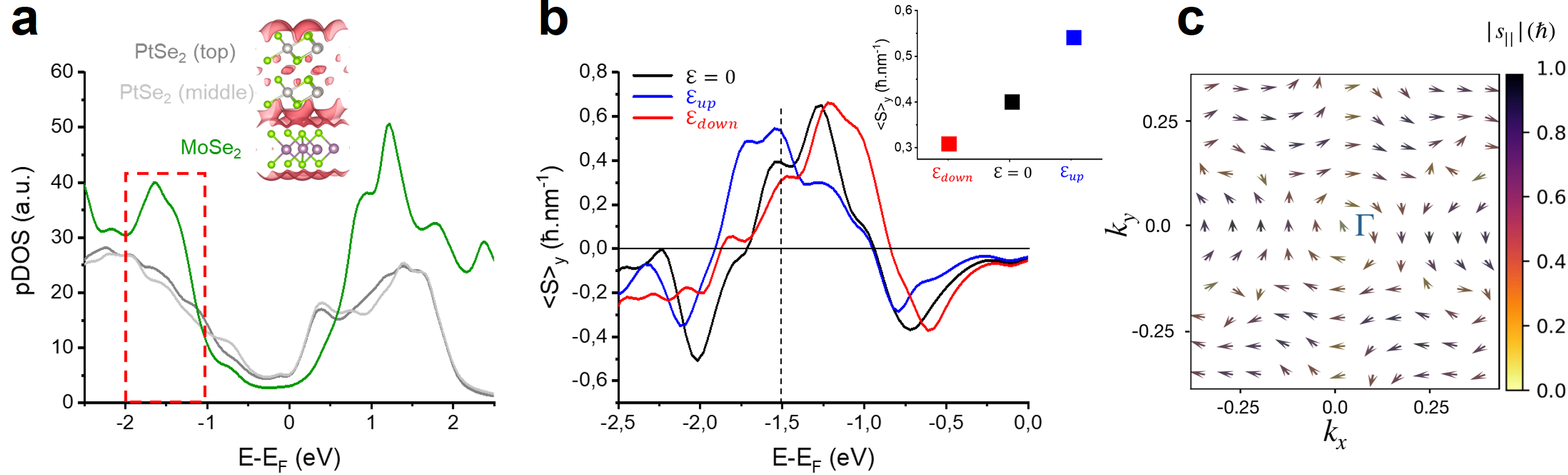
In order to quantify the Rashba effect modulation induced by ferroelectricity, we evaluate in Fig. 4b the spin accumulation response, related to the Rashba Edelstein tensor and thus THz emission, at equilibrium and for an electric field pointing either up or down, in agreement with our experiment. The electric field amplitude is set to 0.25 V/Å, taking into account that LiNbO3 has a larger ferroelectric polarization compared to BaTiO3 and CaO [28, 29]. In the absence of any additional polarization field (=0), a strong and positive spin accumulation is observed in the previously identified energy window, i.e. in the valence band. In the presence of an electric field pointing up (respectively down), the spin accumulation remains positive and is shifted towards lower energy (respectively higher energy), resulting in a total energy shift of about 0.32 eV. Such shift is interpreted from the semi-conducting nature of the layers, which prevents field screening from the substrate, and is in agreement with previous experimental observation of energy shift in ferroelectric/TMD structure [20]. Secondly, we further confirm that in this energy window, there is large range from -2 to -1.4 eV where the spin up accumulation becomes larger than the down one, as depicted in inset of Fig. 4b, in qualitative agreement with our experimental results. The photon energy of our pump laser (1.55eV) corresponds as well to this energy window in the valence band. Interestingly, our results also indicate that the up/down ratio and thus the THz modulation depth could be increased up to 2 by acting on the Fermi level position. Finally, we further confirm that the SCC occurs at MoSe2/PtSe2 interface as the spin accumulation in pristine PtSe2 is negligible (see Suppl. Info. D), in agreement with previous reports [30].
This net spin accumulation results from the existence of Rashba states which are clearly visible when plotting the spin texture in that energy range (Fig. 4c). We thus interpret the observed THz emission change in up and down areas to arise from SCC mediated by IREE at the interface between MoSe2 and PtSe2, and modulated by ferroelectricity. This effect results from a positive spin accumulation and gives the same sign as in the case of Pt, as shown experimentally (Fig. 3c) and confirmed theoretically (see Suppl. Info. E).
Conclusion.
In conclusion, we have presented a large scale heterostructure made of FM/TMD junction on a bi-domain ferroelectric substrate. Using time-domain THz spectroscopy, we found that the THz emission could be modulated by the direction of the out-of-plane ferroelectric polarization. From DFT simulations, we found that the SCC is driven by IREE at the MoSe2/PtSe2 interface, and that the electric field direction allows to shift the semi-conducting bands, resulting in a sizeable change of THz emission. Our results show that the modulation depth could be further increased by varying the Fermi level position, which is reachable by gating the system and applying a voltage to the 2D layers. These findings open very interesting perspectives for the realization of efficient THz modulators based on field effect spin-orbit devices.
Acknowledgements.
The authors acknowledge funding from European Union’s Horizon 2020 research and innovation program under grant agreement No 964735 (FET-OPEN EXTREME-IR). The French National Research Agency (ANR) is acknowledged for its support through the ANR-21-CE24-0011 TRAPIST, ANR-22-EXSP-0003 TOAST, ANR-22-EXSP-0009 SPINTHEORY and ESR/EQUIPEX+ ANR-21-ESRE-0025 2D-MAG projects. The authors also thanks F. Ibrahim, V. Libor and M. Chshiev from SPINTEC for their fruitful help into the calculation of electric field polarization in the 2D materials.The authors declare no competing interests.
References
- Seifert et al. [2022] T. S. Seifert, L. Cheng, Z. Wei, T. Kampfrath, and J. Qi, “Spintronic sources of ultrashort terahertz electromagnetic pulses,” Applied Physics Letters 120, 180401 (2022).
- Seifert et al. [2016] T. Seifert, S. Jaiswal, U. Martens, J. Hannegan, L. Braun, P. Maldonado, F. Freimuth, A. Kronenberg, J. Henrizi, I. Radu, E. Beaurepaire, Y. Mokrousov, P. M. Oppeneer, M. Jourdan, G. Jakob, D. Turchinovich, L. M. Hayden, M. Wolf, M. Münzenberg, M. Kläui, and T. Kampfrath, “Efficient metallic spintronic emitters of ultrabroadband terahertz radiation,” Nature Photonics 10, 483–488 (2016).
- Jungfleisch et al. [2018] M. B. Jungfleisch, Q. Zhang, W. Zhang, J. E. Pearson, R. D. Schaller, H. Wen, and A. Hoffmann, “Control of Terahertz Emission by Ultrafast Spin-Charge Current Conversion at Rashba Interfaces,” Physical Review Letters 120, 207207 (2018).
- Zhou et al. [2018] C. Zhou, Y. Liu, Z. Wang, S. Ma, M. Jia, R. Wu, L. Zhou, W. Zhang, M. Liu, Y. Wu, and J. Qi, “Broadband Terahertz Generation via the Interface Inverse Rashba-Edelstein Effect,” Physical Review Letters 121, 086801 (2018).
- Chen et al. [2019] M. Chen, Y. Wu, Y. Liu, K. Lee, X. Qiu, P. He, J. Yu, and H. Yang, “Current-Enhanced Broadband THz Emission from Spintronic Devices,” Advanced Optical Materials 7, 1801608 (2019).
- Rongione et al. [2023] E. Rongione, L. Baringthon, D. She, G. Patriarche, R. Lebrun, A. Lemaître, M. Morassi, N. Reyren, M. Mičica, J. Mangeney, J. Tignon, F. Bertran, S. Dhillon, P. Le Févre, H. Jaffrès, and J. George, “Spin-Momentum Locking and Ultrafast Spin-Charge Conversion in Ultrathin Epitaxial Bi Sb Topological Insulator,” Advanced Science 10, 2301124 (2023).
- Rho et al. [2023] S. Rho, H. Park, J. Park, K. Jeong, H. Kim, S. Hong, J. Kim, H. W. Lim, Y. Yi, C. Kang, and M. Cho, “Exceptional Spin-to-Charge Conversion in Selective Band Topology of Bi/Bi Sb with Spintronic Singularity,” Advanced Functional Materials 33, 2300175 (2023).
- Gueckstock et al. [2021] O. Gueckstock, L. Nádvorník, M. Gradhand, T. S. Seifert, G. Bierhance, R. Rouzegar, M. Wolf, M. Vafaee, J. Cramer, M. A. Syskaki, G. Woltersdorf, I. Mertig, G. Jakob, M. Kläui, and T. Kampfrath, “Terahertz Spin-to-Charge Conversion by Interfacial Skew Scattering in Metallic Bilayers,” Advanced Materials 33, 2006281 (2021).
- Hawecker et al. [2022] J. Hawecker, E. Rongione, A. Markou, S. Krishnia, F. Godel, S. Collin, R. Lebrun, J. Tignon, J. Mangeney, T. Boulier, J.-M. George, C. Felser, H. Jaffrès, and S. Dhillon, “Spintronic THz emitters based on transition metals and semi-metals/Pt multilayers,” Applied Physics Letters 120, 122406 (2022).
- Rouzegar et al. [2023] R. Rouzegar, A. Chekhov, Y. Behovits, B. Serrano, M. Syskaki, C. Lambert, D. Engel, U. Martens, M. Münzenberg, M. Wolf, G. Jakob, M. Kläui, T. Seifert, and T. Kampfrath, “Broadband Spintronic Terahertz Source with Peak Electric Fields Exceeding 1.5 MV/cm,” Physical Review Applied 19, 034018 (2023).
- Leitenstorfer et al. [2023] A. Leitenstorfer, A. S. Moskalenko, T. Kampfrath, J. Kono, E. Castro-Camus, K. Peng, N. Qureshi, D. Turchinovich, K. Tanaka, A. G. Markelz, M. Havenith, C. Hough, H. J. Joyce, W. J. Padilla, B. Zhou, K.-Y. Kim, X.-C. Zhang, P. U. Jepsen, S. Dhillon, M. Vitiello, E. Linfield, A. G. Davies, M. C. Hoffmann, R. Lewis, M. Tonouchi, P. Klarskov, T. S. Seifert, Y. A. Gerasimenko, D. Mihailovic, R. Huber, J. L. Boland, O. Mitrofanov, P. Dean, B. N. Ellison, P. G. Huggard, S. P. Rea, C. Walker, D. T. Leisawitz, J. R. Gao, C. Li, Q. Chen, G. Valušis, V. P. Wallace, E. Pickwell-MacPherson, X. Shang, J. Hesler, N. Ridler, C. C. Renaud, I. Kallfass, T. Nagatsuma, J. A. Zeitler, D. Arnone, M. B. Johnston, and J. Cunningham, “The 2023 terahertz science and technology roadmap,” Journal of Physics D: Applied Physics 56, 223001 (2023).
- Ji et al. [2023] R. Ji, M. T. Hibberd, C.-H. Lin, D. A. Walsh, T. Thomson, P. W. Nutter, and D. M. Graham, “Tunable multi-cycle terahertz pulse generation from a spintronic emitter,” Applied Physics Letters 123, 212402 (2023).
- Nkeck et al. [2022] J. E. Nkeck, L.-P. Béliveau, X. Ropagnol, D. Deslandes, D. Morris, and F. Blanchard, “Parallel generation and coding of a terahertz pulse train,” APL Photonics 7, 126105 (2022).
- Ning et al. [2022] S. Ning, H. Liu, J. Wu, and F. Luo, “Challenges and opportunities for spintronics based on spin orbit torque,” Fundamental Research 2, 535–538 (2022).
- Noël et al. [2020] P. Noël, F. Trier, L. M. Vicente Arche, J. Bréhin, D. C. Vaz, V. Garcia, S. Fusil, A. Barthélémy, L. Vila, M. Bibes, and J.-P. Attané, “Non-volatile electric control of spin–charge conversion in a SrTiO3 Rashba system,” Nature 580, 483–486 (2020).
- Hirori et al. [2011] H. Hirori, A. Doi, F. Blanchard, and K. Tanaka, “Single-cycle terahertz pulses with amplitudes exceeding 1 MV/cm generated by optical rectification in LiNbO3,” Applied Physics Letters 98, 091106 (2011).
- Zhang et al. [2021] B. Zhang, Z. Ma, J. Ma, X. Wu, C. Ouyang, D. Kong, T. Hong, X. Wang, P. Yang, L. Chen, Y. Li, and J. Zhang, “1.4-mJ High Energy Terahertz Radiation from Lithium Niobates,” Laser & Photonics Reviews 15, 2000295 (2021).
- Rao et al. [2016] A. Rao, A. Patil, P. Rabiei, A. Honardoost, R. DeSalvo, A. Paolella, and S. Fathpour, “High-performance and linear thin-film lithium niobate Mach–Zehnder modulators on silicon up to 50 GHz,” Optics Letters 41, 5700 (2016).
- Abdukayumov et al. [2024] K. Abdukayumov, M. Mičica, F. Ibrahim, L. Vojáček, C. Vergnaud, A. Marty, J. Veuillen, P. Mallet, I. G. De Moraes, D. Dosenovic, S. Gambarelli, V. Maurel, A. Wright, J. Tignon, J. Mangeney, A. Ouerghi, V. Renard, F. Mesple, J. Li, F. Bonell, H. Okuno, M. Chshiev, J. George, H. Jaffrès, S. Dhillon, and M. Jamet, “Atomic-Layer Controlled Transition from Inverse Rashba–Edelstein Effect to Inverse Spin Hall Effect in 2D PtSe Probed by THz Spintronic Emission,” Advanced Materials 36, 2304243 (2024).
- Salazar et al. [2022] R. Salazar, S. Varotto, C. Vergnaud, V. Garcia, S. Fusil, J. Chaste, T. Maroutian, A. Marty, F. Bonell, D. Pierucci, A. Ouerghi, F. Bertran, P. Le Fèvre, M. Jamet, M. Bibes, and J. Rault, “Visualizing Giant Ferroelectric Gating Effects in Large-Scale WSe /BiFeO Heterostructures,” Nano Letters 22, 9260–9267 (2022).
- Dau et al. [2019] M. T. Dau, C. Vergnaud, M. Gay, C. J. Alvarez, A. Marty, C. Beigné, D. Jalabert, J.-F. Jacquot, O. Renault, H. Okuno, and M. Jamet, “van der Waals epitaxy of Mn-doped MoSe2 on mica,” APL Materials 7, 051111 (2019).
- Dang et al. [2020] T. H. Dang, J. Hawecker, E. Rongione, G. Baez Flores, D. Q. To, J. C. Rojas-Sanchez, H. Nong, J. Mangeney, J. Tignon, F. Godel, S. Collin, P. Seneor, M. Bibes, A. Fert, M. Anane, J.-M. George, L. Vila, M. Cosset-Cheneau, D. Dolfi, R. Lebrun, P. Bortolotti, K. Belashchenko, S. Dhillon, and H. Jaffrès, “Ultrafast spin-currents and charge conversion at 3 d -5 d interfaces probed by time-domain terahertz spectroscopy,” Applied Physics Reviews 7, 041409 (2020), number: 4.
- Li et al. [2009] D. Li, G. Ma, J. Ge, S. Hu, and N. Dai, “Terahertz pulse shaping via birefringence in lithium niobate crystal,” Applied Physics B 94, 623–628 (2009).
- Rongione et al. [2022] E. Rongione, S. Fragkos, L. Baringthon, J. Hawecker, E. Xenogiannopoulou, P. Tsipas, C. Song, M. Mičica, J. Mangeney, J. Tignon, T. Boulier, N. Reyren, R. Lebrun, J. George, P. Le Fèvre, S. Dhillon, A. Dimoulas, and H. Jaffrès, “Ultrafast Spin-Charge Conversion at SnBi Te /Co Topological Insulator Interfaces Probed by Terahertz Emission Spectroscopy,” Advanced Optical Materials 10, 2102061 (2022).
- Carletti et al. [2023] L. Carletti, C. McDonnell, U. Arregui Leon, D. Rocco, M. Finazzi, A. Toma, T. Ellenbogen, G. Della Valle, M. Celebrano, and C. De Angelis, “Nonlinear THz Generation through Optical Rectification Enhanced by Phonon–Polaritons in Lithium Niobate Thin Films,” ACS Photonics 10, 3419–3425 (2023).
- Xu et al. [2024] L. Xu, Q. Zeng, S. Xiong, Y. Zhang, L. Cao, J. Tao, Z. Li, L.-L. Wang, and K. Dong, “Two-dimensional mose2/ptse2 van der waals type-ii heterostructure: Promising visible light photocatalyst for overall water splitting,” International Journal of Hydrogen Energy 50, 352–364 (2024).
- Kandemir et al. [2018] A. Kandemir, B. Akbali, Z. Kahraman, S. V. Badalov, M. Ozcan, F. Iyikanat, and H. Sahin, “Structural, electronic and phononic properties of ptse2: from monolayer to bulk,” Semiconductor Science and Technology 33, 085002 (2018).
- Vyas, Patel, and Bhatt [2023] P. Vyas, A. B. Patel, and N. K. Bhatt, “First-principles study of thermoelasticity and structural phase diagram of CaO,” Physical Review B 107, 014107 (2023).
- Novak, Pirc, and Kutnjak [2014] N. Novak, R. Pirc, and Z. Kutnjak, “Effect of Electric Field on Ferroelectric Phase Transition in BaTiO Ferroelectric,” Ferroelectrics 469, 61–66 (2014).
- Mudgal et al. [2023] R. Mudgal, A. Jakhar, P. Gupta, R. S. Yadav, B. Biswal, P. Sahu, H. Bangar, A. Kumar, N. Chowdhury, B. Satpati, B. R. Kumar Nanda, S. Satpathy, S. Das, and P. K. Muduli, “Magnetic-proximity-induced efficient charge-to-spin conversion in large-area ptse2/ni80fe20 heterostructures,” Nano Letters 23, 11925–11931 (2023).
- Perdew et al. [1992] J. P. Perdew, J. A. Chevary, S. H. Vosko, K. A. Jackson, M. R. Pederson, D. J. Singh, and C. Fiolhais, “Atoms, molecules, solids, and surfaces: Applications of the generalized gradient approximation for exchange and correlation,” Phys. Rev. B 46, 6671–6687 (1992).
- Perdew, Burke, and Ernzerhof [1996] J. P. Perdew, K. Burke, and M. Ernzerhof, “Generalized gradient approximation made simple,” Phys. Rev. Lett. 77, 3865–3868 (1996).
- Soler et al. [2002] J. M. Soler, E. Artacho, J. D. Gale, A. García, J. Junquera, P. Ordejón, and D. Sánchez-Portal, “The siesta method for ab initio order- n materials simulation,” J. Phys.: Condens. Matter 14, 2745 (2002).
- Fernández-Seivane et al. [2007] L. Fernández-Seivane, M. A. Oliveira, S. Sanvito, and J. Ferrer, “On-site approximation for spin–orbit coupling in linear combination of atomic orbitals density functional methods,” J. Phys.: Condens. Matter 19, 489001 (2007).
- Troullier and Martins [1991] N. Troullier and J. L. Martins, “Efficient pseudopotentials for plane-wave calculations,” Phys. Rev. B 43, 1993–2006 (1991).
Supplementary Material of "Inverse Rashba Edelstein THz emission modulation induced by ferroelectricity in CoFeB/PtSe2/MoSe2//LiNbO3 systems". January 7, 2025
S. Massabeau
O. Paull
A. Pezo
F. Miljevic
M. Mičica
A. Grisard
P. Morfin
R. Lebrun
H. Jaffrès
S. Dhillon
J.-M. George
M. Jamet
M. Bibes
Appendix A Surface characterization
In order to ensure the MoSe2/PtSe2 interface quality after the transfer process, We first check on the LiNbO3 surface quality before transfer. As depicted in Fig. 5, we found a very low roughness with a RMS of 0.33 nm.
Appendix B Spin accumulation and spin texture calculations
DFT simulations were carried out using the Perdew-Burke-Ernzerhof (PBE) [31, 32] exchange-correlation functional. We perform the geometry optimizations employing a localized atomic basis based on SIESTA [33] with an atom-centered double- plus polarization (DZP) basis sets considering an energy cut-off for the real-space mesh of 400 Ry. Relativistic effects were introduced via the off-site approximation [34] using fully-relativistic norm-conserving pseudopotentials [35]. The system’s ground state properties are obtained after performing a full self-consistent cycle converged on a -points sampling of the Brillouin zone, using a 25 Å vacuum distance between periodic images to avoid spurious effects. The lattice constant is fixed to that of PtSe2, corresponding to a supercell of size 6.57 Å having a MoSe2 supercell. We used the conjugate gradient algorithm to minimize the atomic forces below 0.01 eV/Å with the inclusion of VdW corrections as implemented in the DFT code.
The spin texture shown in Fig. 4c was calculated using:
where is an eigenstate of the Hamiltonian and the Overlap matrix has to be considered as the basis is non-orthogonal. The matrices are the usual spin operator matrices proportional to the Pauli matrices. Analogously, the spin accumulations was obtained by using linear response theory:
| (1) |
where is the velocity operator modified for treating a non-orthogonal basis as:
| (2) |
which for our case was taken in the parallel to bilayer structure representing the external perturbation and is the operator corresponding to the spin degree of freedom. In order to achieve convergence in the transport calculations we have considered a mesh-grid for sampling the Brillouin Zone (BZ) where 1 was integrated.
Appendix C Band structure of the trilayer system
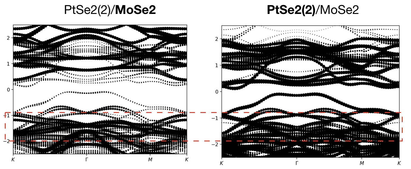
We present on Fig. 6 the band structure of the MoSe2(1ML)/PtSe2(2ML) trilayer, projecter either on MoSe2 (left) or PtSe2 (right). From our DFT simulations, we see that by considering a PtSe2 bilayer we get a reduced gap, in agreement with previous studies [27]. This would allow spin-to-charge conversion near the Fermi level, provided the existence of PtSe2 states. On the other hand, when MoSe2 is considered, overlap between states coming from both systems occur only below -1 eV (dashed red rectangle) and for higher energies above the Fermi level. This characteristic is also highlighted by calculating the projected density of states, as shown in Fig. 4.a in the main text.
Appendix D Spin accumulation in pristine PtSe2
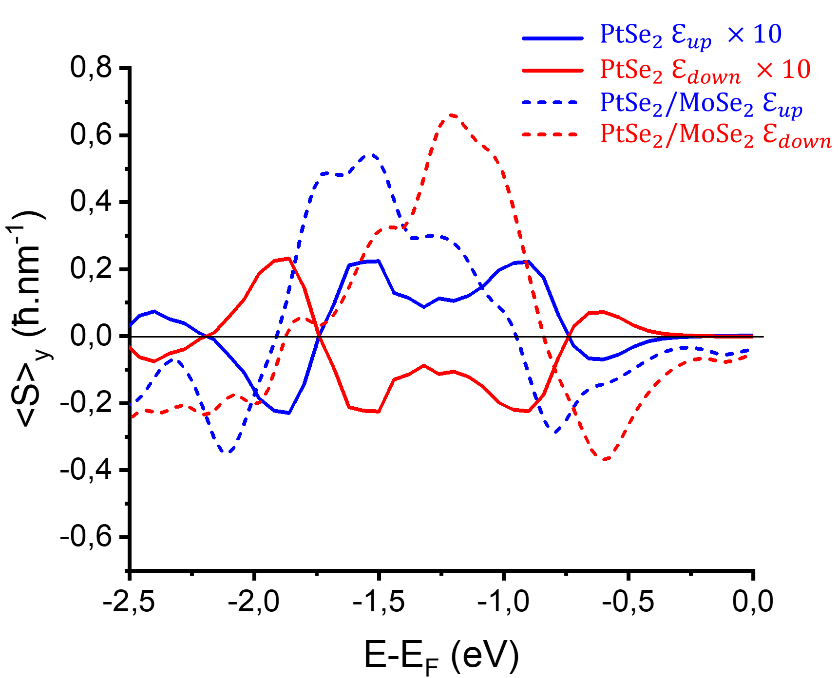
In Fig. 7, we show the calculation of spin accumulation, related to the Rashba Edelstein tensor, for pure PtSe2 when an electric field is applied, using the same electric field as that in the main text for the trilayer system MoSe2(1ML)/PtSe2(2ML). Although the inversion symmetry breaking on PtSe2 leads to a non-vanishing value of the spin accumulation (plain lines), its value is at least one order of magnitude smaller than the effect when MoSe2 is added (dashed lines), meaning that the main effect responsible for the SCC in the trilayer system comes from the hybridized orbitals between PtSe2 and MoSe2. Furthermore, we clearly see a reversal of the REE tensor when the electric field is reversed in the case of pure PtSe2, since the Rashba effect captures the chirality related to the direction on which inversion symmetry is broken. This is contrast with the situation depicted in the MoSe2(1ML)/PtSe2(2ML) trilayer where there’s no such reversal in the sign of the tensor. This result is in agreement with previous report on negligible Rashba effect in FM/PtSe2 structures [30], and further corroborates our assumption that SCC happens in the valence bands [19] due to a strong orbital hybridization between PtSe2 and MoSe2.
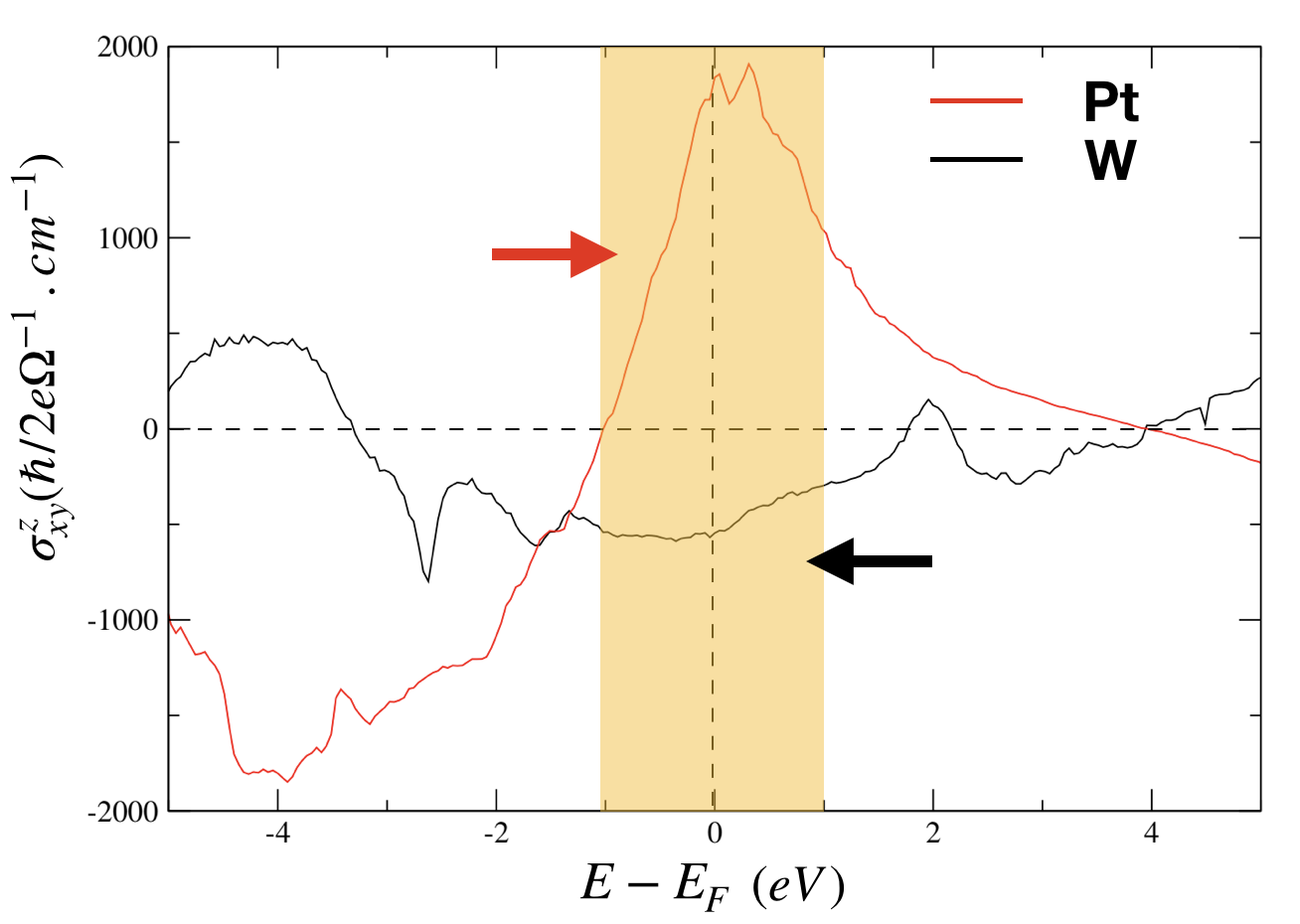
Appendix E Conversion sign comparison with Pt and Co
In order to compare the conversion sign obtained from spin accumulation modelling in MoSe2(1ML)/PtSe2(2ML) systems, we calculate the spin Hall conductivity of Pt and W. In the case of systems made of FM/Pt and FM/W, the SCC is driven by Inverse Spin Hall Effect, and the THz emission is directly proportionnal to the spin Hall conductivity, with a positive value for Pt (sets by convention) and an opposite one (negative) for W.
From our calculation, we recover Pt spin Hall conductivity to be positive, with W exhibiting an opposite phase, nearby the Fermi level. As we experimentally found SCC in our heterostructure to be the same sign as of Pt, we conclude that positive values for spin accumulation define the relevant energy window involved in the conversion process.