Two superconducting thin films systems with potential integration of different quantum functionalities
Abstract
Quantum computation based on superconducting circuits utilizes superconducting qubits with Josephson tunnel junctions. Engineering high-coherence qubits requires materials optimization. In this work, we present two superconducting thin film systems, grown on silicon (Si), and one obtained from the other via annealing. Cobalt (Co) thin films grown on Si were found to be superconducting [EPL 131 (2020) 47001]. These films also happen to be a self-organised hybrid superconductor/ferromagnet/superconductor (S/F/S) structure. The S/F/S hybrids are important for superconducting -qubits [PRL 95 (2005) 097001] and in quantum information processing. Here we present our results on the superconductivity of a hybrid Co film followed by the superconductivity of a CoSi2 film, which was prepared by annealing the Co film. CoSi2, with its noise about three orders of magnitude smaller compared to the most commonly used superconductor aluminium (Al), is a promising material for high-coherence qubits. The hybrid Co film revealed superconducting transition temperature = 5 K and anisotropy in the upper critical field between the in-plane and out-of-plane directions. The anisotropy was of the order of ratio of lateral dimensions to thickness of the superconducting Co grains, suggesting a quasi-2D nature of superconductivity. On the other hand, CoSi2 film showed a of 900 mK. In the resistivity vs. temperature curve, we observe a peak near . Magnetic field scan as a function of shows a monotonic increase in intensity of this peak with temperature. The origin of the peak has been explained in terms of parallel resistive model for the particular measurement configuration. Although our CoSi2 film contains grain boundaries, we observed a perpendicular critical field of 15 mT and a critical current density of 3.8107 A/m2, comparable with epitaxial CoSi2 films.
Keywords: Superconductivity, upper critical field, critical current, van der Pauw, inhomogeneity, coherence length
1 Introduction
Superconductivity plays a pivotal role in quantum technology, especially in quantum computers. The basic unit of a quantum computer is a quantum bit (or qubit), which can be implemented via several physical platforms. However, superconducting qubit is one of the most promising approaches towards building a scalable fault-tolerant quantum computer [1, 2]. Superconducting qubit technology uses several superconducting materials, such as Al, Nb, Ta etc. for the fabrication of qubits, capacitor pads and resonators. One of the major aims of materials research in this area is to develop superior qubits with longer decoherence time. The main component of a superconducting qubit is a Josephson junction (JJ), which is a superconductor/insulator/superconductor (S/I/S) heterostructure [3]. Although, several superconductors are used for building superconducting quantum computers, Al is the most widely used superconducting material for the fabrication of qubits and quantum processors. Aluminum-based qubits use Al/AlOx/Al heterostructures as JJs. Since the quantum states are intrinsically fragile, interactions of qubits with the environment result in various sources of noise which lead to decoherence. Suppressing decoherence, or increasing decoherence time, involves a synchronous optimization of both electromagnetic design and materials quality [4]. Besides the improvement of qubit design and microwave engineering, it is desirable to use superconductors with superior material properties. One important source of noise, responsible for qubit decoherence, is the noise [4] originating from the interfaces and surfaces of the materials and heterostructures used for fabricating the qubits. Recently it was shown that cobalt disilicide (CoSi2), a superconductor with comparable superconducting transition temperature () to that of Al [5], has two to three orders of magnitude less noise compared to Al. It was conjectured that CoSi2 films may provide superior qubits with longer decoherence time compared to Al [5].
CoSi2 has already been used for decades as metallic contacts in semiconductor technology [6, 7]. CoSi2 is usually produced by depositing thin films of cobalt (Co) on silicon (Si) followed by post-deposition annealing [6, 8], or by directly depositing Co on hot Si substrates [9, 10]. Out of these two materials - Co and CoSi2 - although CoSi2 is a superconductor [5, 11], Co was neither known nor expected to be a superconductor as cobalt is a ferromagnetic metal, and materials possessing long range magnetic order do not exhibit superconductivity [12]. In some cases, such ferromagnetic materials, for example iron (Fe), can show superconductivity under high pressure [13]. However, bulk Co was not shown to be a superconductor under any condition. Very recently, superconductivity was discovered in Co thin films grown on Si [14]. Normal Co has a hexagonal close packed (hcp) crystal structure and is ferromagnetic. In the thin films, grown on clean Si substrates, a high-density non-magnetic (HDNM) face-centered cubic (fcc) phase of Co was found to have grown [15, 16]. While normal Co is not superconducting, this HDNM phase of Co is superconducting [14]. Earlier, theoretically it was predicted that at a high-density the fcc phase of Co would lose magnetism [17], although no superconductivity was predicted. However, the theoretical work carried out together with the experimental discovery of superconductivity in Co shows that at certain densities of fcc Co, it becomes non-magnetic as well as superconducting, and a detailed phase diagram has been produced. This phase diagram shows the range of densities and strains in the thin films for which superconductivity would be observed [14]. Another interesting aspect of these Co films is that the whole film is not superconducting. The films have a self-organised hybrid three-layer structure HDNM-Co/Normal-Co/HDNM-Co [15, 16]. While the normal-Co is a ferromagnet (F), the HDNM-Co layers are superconductors (S). Thus, the Co films have an S/F/S hybrid structure. Such S/F/S hybrid structures have superconducting-spintronic and other applications in quantum technology, such as in quantum information processing [18, 19]. S/F/S structures have also shown 0- quantum phase transition [20]. An S/F/S structure forms a ferromagnetic JJ (or -JJ), which can be used to fabricate a superconducting -qubit with a long decoherence time. Such a superconducting -qubit may be a superconducting ring with one -JJ and one normal JJ (or 0-JJ) structures [21]. 0- qubits can be implemented in different ways. Recently, an intrinsically error-protected superconducting 0- qubit with a long decoherence time (1.6 ms) has been experimentally realized [22].
Thus, both the superconducting systems, Co and CoSi2, have potential applications in quantum technology. With the possibility of localized pulsed laser annealing of a Co film on Si to form CoSi2 [23], realization of devices incorporating functionalities of both the superconductors Co and CoSi2, on the same Si substrate can be envisaged.
In this article, we explore the conversion of one superconducting system (Co) to another superconductor (CoSi2), achieved via annealing and compare their superconducting properties with a view to utilize the latter in superconducting quantum circuits.
2 Experimental methods
Co films were deposited using electron beam evaporation onto a (100)-oriented n-type Si substrate (resistivity 3 - 8.5 .cm) at room temperature under high vacuum. Prior to deposition, the Si substrate was cleaned in 1% aq. HF solution to etch-off the native oxide (SiOx) layer. Earlier investigations have shown that this method of growth produces polycrystalline Co films, which are also superconducting [14, 15]. To investigate the superconductivity in the Co film, electrical resistivity measurements were performed using conventional linear four-probe technique (with indium-silver solder contacts) under externally applied magnetic fields inside a commercial physical property measurement system (PPMS of M/s. Quantum Design) down to low temperature (2 K). To apply magnetic fields along different directions with respect to the film (sample) plane, the sample was rotated using a rotator-puck/sample-insert provided with the PPMS. This has allowed us to measure critical field anisotropy, which was not investigated in earlier studies [14].
Following that, the superconducting Co film was converted into a superconducting CoSi2 film via annealing at 850 oC under high vacuum (HV) conditions ( 5 mbar) for 1.5 hours. To investigate the superconductivity of the CoSi2 film, resistivity measurements were carried out using van der Pauw (vdP) technique inside a dilution refrigerator that could cool down to 30 millikelvin. The contact pads for the vdP configuration were prepared by thermal evaporation of Ti/Au, patterned by lift-off photolithography. The magnetic field could only be applied in the out-of-plane direction with the available sample space configuration inside the dilution refrigerator.
X-ray characterizations of both the Co film and the CoSi2 film were done at room temperature in a Rigaku SmartLab diffractometer with Cu-Kα x-rays ( = 1.5406 Å). X-ray reflectivity (XRR) was performed on the Co film to determine its thickness, roughness and electron densitiy distribution (layer structure), while grazing incidence x-ray diffraction (GIXRD) was performed on both the Co and the CoSi2 films to identify their phases. Moreover, cross-sectional high resolution transmission electron microscopy (HRTEM) was performed on the CoSi2 film to investigate the thickness and crystal orientation of the film with respect to the substrate.
3 Results and Discussions
3.1 Cobalt film
3.1.1 Characterization
Figure 1 (a) shows GIXRD of the film, indicating the (0002) peak of Co. This indicates that the hcp phase of normal Co dominates the film. On the other hand, in order to get the information of the overall film stack (i.e., thickness, individual layer densities, surface and interfacial roughness), XRR data were carefully analyzed, since it can reveal the electron scattering length density (ESLD) or electron density depth profile (proportional to mass density depth profile) with very high depth resolution ( 1 Å), and rms roughness parameters in the direction normal to the film plane.
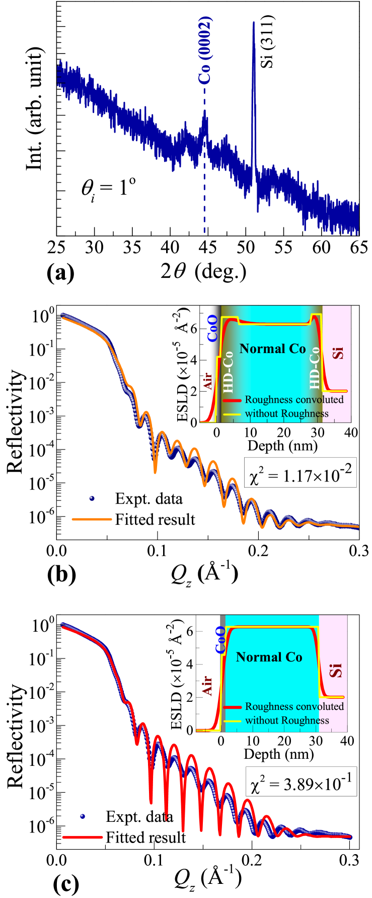
We obtained a total thickness of 30.89(3) nm for the Co film from the XRR measurement. The best fit to the XRR data ( = 1.17), as shown by solid orange-colored line in Fig. 1(b), was obtained by considering a ESLD profile that shows
| Layer |
|
|
|
||||||
|---|---|---|---|---|---|---|---|---|---|
| CoO | 1.27(9) | 4.53(7) | 1.4(6) | ||||||
| HD-Co | 1.61(7) | 6.87(1) | 1.2(9) | ||||||
| Normal Co | 24.47(2) | 6.27(3) | 1.0(0) | ||||||
| HD-Co | 3.52(5) | 6.70(5) | 0.5(5) | ||||||
| Si substrate | — | 2.01(5) | 1.0(3) |
higher ESLDs at the Co/Si interface as well as near the Co/CoO interface (shown in the inset of the the panel) [A CoO layer (2 nm) naturally grows on the Co film after removing it from the vacuum chamber following film deposition]. This kind of hybrid three-layer structure HDNM-Co/Normal-Co/HDNM-Co forms in a self-organised manner, similar to those reported in Ref. [15, 16]. The method of detailed analysis may be found in Refs. [15, 16]. The ESLD, thickness and roughness parameters obtained from XRR of the present sample are given in Table 1. In our case, we obtained a layer of ESLD = 6.87(0) 10-5 Å-2 (of thickness 1.27(9) nm) close to the Co/CoO interface and another layer of ESLD = 6.70(5) 10-5 Å-2 (of thickness 3.52(5) nm) at the Co/Si interface, both of which are higher in density compared to that of Normal-Co layer (of thickness 24.47(2) nm) in the middle. [For comparison, we show that the XRR data could not be fitted properly assuming a single uniform density Normal Co layer (ESLD = 6.27(3) 10-5 Å-2) (with obvious CoO layer on top) along the whole depth of the film, as shown in Fig. 1 (c)]. Such HDNM Co layers in the obtained tri-layer structure are non-magnetic with nanoscale grains [15, 16] and show inhomogeneous superconductivity as reported in Ref. [14]. Since the nature of superconductivity was reported to be inhomogeneous in nature, this stimulated us to investigate the superconducting behavior with variation of direction of magnetic field, as described below.
3.1.2 Transport properties
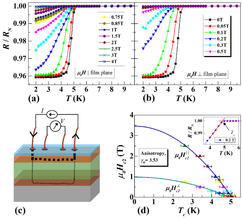
To investigate the nature of superconductivity, we measure the temperature variation of resistance (down to = 2 K only) under various magnetic field strengths applied parallel (IP) and perpendicular (OOP) to the film plane. The results are presented in Fig. 2(a) and (b). We observe that the superconductivity is remarkably suppressed by a magnetic field of 2 T and 0.5 T applied IP and OOP, respectively.
However, one of the important features of these resistance () vs temperature () (or ) curves is the non-vanishing resistance in the superconducting state (i.e., below , even in the absence of magnetic field). There can be three possibile contributions to this non-zero resistance: (i) due to presence of a comparatively higher resistive CoO layer at the top; (ii) due to contact resistance of the probes and sensitivity of the measuring instruments [24]; or (iii) due to granular nature of the sample itself [25, 26]. Moreover, our sample has superconducting Co layers in the background of a normal Co layer. In our sample, there is only 4 drop in resistance in the superconducting state with respect to the normal state. This can be explained considering the resistance contribution from the CoO layer and the normal Co layer [schematically shown in Fig. 2(c)], even if we neglect the contact resistance. It should be noted that the non-zero resistance in the superconducting state of granular metals might also be attributed to Josephson coupling between an increasing number of pairs of grains with decreasing temperature [25, 26, 27, 28].
By virtue of competition between the Josephson coupling energy () and capacitive coupling energy () between the grains, the superconducting state appears when .
To generate the phase diagram, we first define the critical temperature () as the temperature where superconductivity sets in (onset of superconductivity) (as shown in the inset of Fig. 2(d) with an arrow). Thus we generate the phase diagram from the plots as shown in the main panel of Fig. 2(d), which reveals a clear anisotropy in the upper critical field along the two directions. We determine these upper critical fields namely (0) and (0) from fitting, using the BCS model:
| (1) |
where (0) is the zero temperature upper critical field and is the absolute critical temperature. We also define the anisotropy in the upper critical field as:
| (2) |
|
|
|
|
|||||||||
|---|---|---|---|---|---|---|---|---|---|---|---|---|
| IP () | 3.46(6) | 5.03(1) | 3.53 | 9.75(3) | ||||||||
| OOP () | 0.98(4) | 4.94(5) | 18.32(2) |
The obtained values are summarized in Table 2. In comparison to robust 2D superconducting systems where anisotropy is quite strong ( 10), the anisotropy of our system ( 3.5) indicates a quasi-2D nature of superconductivity in it. We have layered superconducting regions (or grains) of HDNM Co whose aspect ratio of lateral dimension ( 10 nm) to thickness ( 3 nm) [15] is almost 3. Therefore it is expected that the coherence length along the film-normal is longer than that along the film-plane, which induces an anisotropic pair-breaking mechanism depending on the direction of the magnetic field applied to the film. This explains anisotropy in the upper critical fields.
In case of the orbital-limiting effect, which is dominant under perpendicular (OOP) magnetic fields, Cooper pair breaking is induced by the momentum, , where is the vector potential, and eventually, the kinetic energy of supercurrent exceeds the superconducting gap energy [29, 30]. Thus, the upper critical field is recognized as the orbital-limiting field, = /(), which depends on the coherence length of Cooper pair, . Here is the magnetic flux quantum.
On the other hand, for a 2D weak coupling BCS superconductor, the upper critical field becomes limited by the so called Pauli paramagnetic limit (or the Chandrasekhar-Clogston limit) [31, 32], where the Zeeman splitting energy of individual electron spin exceeds the superconducting energy gap and thus Cooper pair becomes energetically unstable. This Pauli limiting field becomes important under parallel (IP) magnetic fields and is given by , where and are the Boltzmann’s constant and Bohr magneton, respectively. Taking = 5 K, we have = 9.2 T, which is way larger than the (0) of our Co film suggesting a very weak coupling regime of superconductivity.
3.2 CoSi2 film
We now turn towards the CoSi2 film formed by annealing of the Co / Si thin film system discussed so far.
3.2.1 Characterization
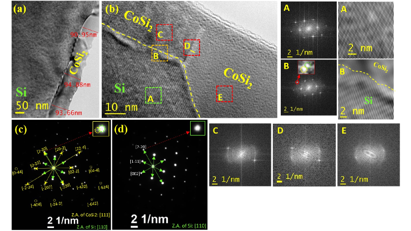
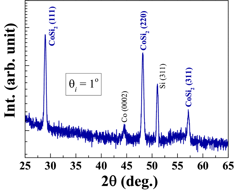
Figure 3 shows the GIXRD pattern of the annealed sample. The peaks at 28.84o, 48.12o and 57.18o correspond to the (111), (220), and (311) orientations of CoSi2 and confirm that the CoSi2 phase has already formed with 1.5 hours of annealing at 850 oC and manifest good crystallinity of the film. To get further information about the crystalline nature of the film, the cross-sectional HRTEM of the film has been performed, as shown in Fig. 4(a)-(d). From the low magnification image [Fig. 4(a)], the overall film thickness is found to be around 90 nm. The high magnification HRTEM image in Fig. 4(b) further confirms that the film has multiple CoSi2 grains. The relative orientation of the CoSi2 film with respect to the Si substrate can be visualised from the SAED pattern in figure panel (c). For comparison the SAED pattern of the Si substrate is shown in panel (d). In this film, (111) planes of CoSi2 is parallel to (110) planes of Si. To get further insight into the detailed crystallinity, the fast Fourier transform (FFT) has been performed in various regions as marked by (A) to (E) of the image in Fig. 4(b) and are shown in the corresponding sub-panels. It is interesting to note the changes in the FFT diffraction patterns as we go from one grain to the other across the grain boundary [sub-panels (C) to (E)]. This confirms the different orientations of the two grains separated by the grain boundary. It should be noted that two such superconducting grains, separated by a grain boundary, can behave as an inherent Josephson junction, the effects of which can be seen in the resistivity and characteristics of the sample.
3.2.2 Transport Properties
A. Resistivity
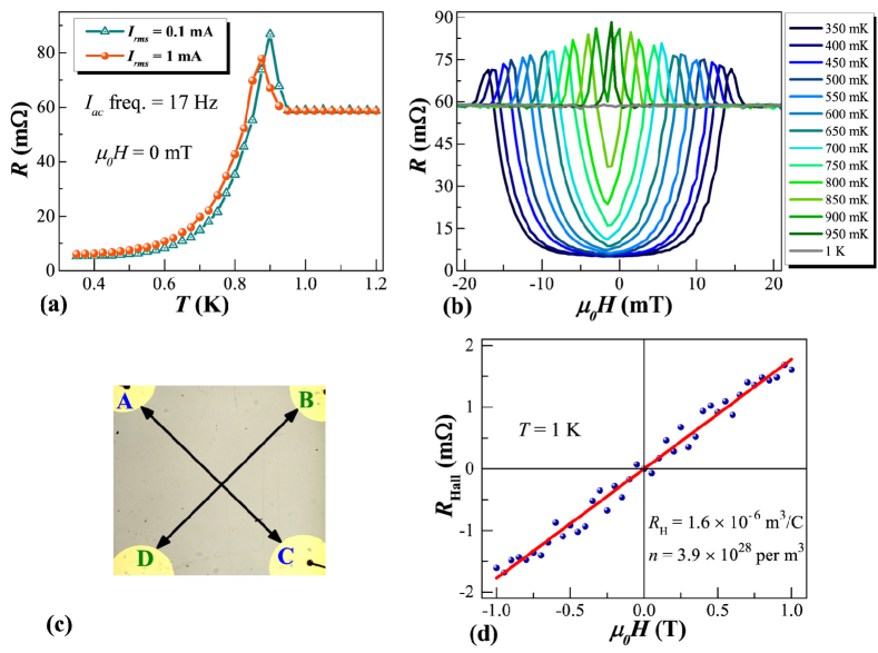
The temperature dependence of the resistance () of the CoSi2 film measured in van-der Pauw technique for two different currents under zero magnetic field is presented in Fig. 5 (a). Firstly, we observe a superconducting transition around 900 mK with a prominent peak near the transition temperature. Secondly, although there is almost an order of magnitude drop in resistance in the superconducting state with respect to the normal state, the resistance value in the superconducting state is still non-zero. This again hints towards the Josephson coupling between the superconducting grains, which we will discuss later.
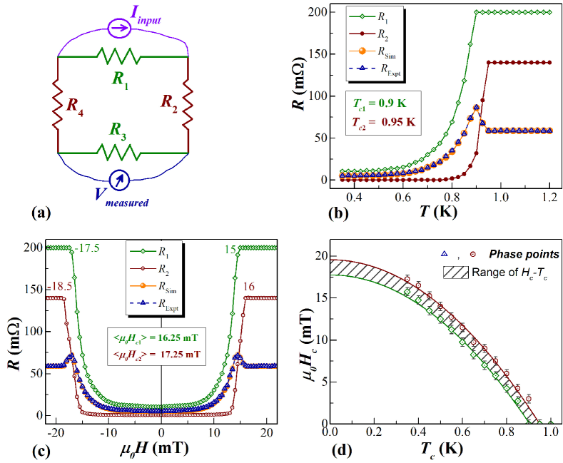
The peak in the resistive transition is easily reproduced by considering simultaneously the inhomogeneity of the sample and the geometry of the electrical probes. Assuming a simple equivalent circuit representation with normal state resistances , , , and between each couple of probes in the vdP configuration as in Fig. 6(a), the measured resistance = / is given by [33, 34]
| (3) |
Because of the inhomogeneity of our sample, the four resistors can have different . For simplicity, we further assume that = and = at all temperatures. Then, using Eq.3 we fit the zero-magnetic-field curve as shown in Fig. 6(b).
Similar to the curve in Fig. 5 (a), we notice a peak in resistance near the critical magnetic field in the curve in Fig. 5 (b). In order to explain this behaviour, it is reasonable to argue that two zones having different , as described in previous paragraph, are also characterized by different critical magnetic fields.
To fit the and curve we justify our arguments as follows:
(i) The regions with higher normal state resistance () behave as more inhomogeneous region with lower and lower ; and conversely the regions with low will have higher and higher [33, 26],
(ii) Apart from the measure of , the degree of inhomogeneity can be evaluated qualitatively from the width of the transition: a higher inhomogeneity implies a wider transition [35].
Considering the above arguments, we first fit the zero field curve by taking = 0.95 K = 0.9 K. Accordingly, we relate the slight difference of 50 mK to the presence of inhomogeneity/disorder [36], and thus have , where is the critical magnetic field of the zone described by the resistor . Using this argument, we fit the curve at zero temperature [see Fig. 6(c)]. From these fits, we note that the two ’s are located one at the peak point of the experimental curve and the other at the point where the normal state resistance is just reached. Utilizing this observation, we extract the pair of values of at different temperatures from the experimental curves and generate the phase diagram as shown in Fig. 6(d). We further note that the phase diagram does not present a sharp boundary between the normal and superconducting state, rather a broad region (shaded area in the figure), where the experimentally extracted values represent the two limits of the phase boundary. We then fit the data using the BCS model (as in Eq. 1) and find the highest critical field (0) 20 mT, comparable to previous results on CoSi2 films [37, 38].
We also measured the Hall effect in the CoSi2 film at normal state ( = 1 K) as shown in Fig. 5(c) and (d), which indicates that the charge carriers are holes, in consistency with previous results [5, 39]. We found the Hall coefficient = 1.6 10-6 /C, hole concentration = 3.9 1028 m-3 and a Hall mobility = 1.18 T-1. From this, we estimated the Fermi wave vector [= (3)1/3] 1.05 1010 m-1 and a Fermi velocity of 1.22 106 m/s [5, 40, 41]. We further calculated the mean free path, = 6.12 10-10 m from the longitudinal resistivity () using the relation: = 3/(), and estimated the disorder factor 6.43. Accordingly, the high value of = 1.6 10-6 /C in our CoSi2 film is consistent with the low value of in comparison with recent reports on polycrystalline CoSi2 film [39].
B. I-V characteristics

To find the critical current (), we measured the characteristics of the CoSi2 film at various temperatures under zero magnetic field, as shown in Fig. 7(a). Instead of a sharp transition to a normal state (recognised by linear region), we observe exponential type of behaviour, which probably is due to presence of inhomogeneity [42, 43]. The linear region above a certain (critical) current indicates the normal state region. Interestingly we also observe a peculiar hump near the critical current. By considering the equivalent resistor circuit as in Fig. 6(a), we can argue that the hump in characteristics occurs due to two different critical currents of the two different resistive regions [34] ( and ) as shown in Fig. 7(b) (left axis). The critical currents can be best extracted from the d/d vs curves as shown in Fig. 7(b) (right axis). From each curves in Fig. 7(a), we determine the corresponding and values and thus generate the phase diagram at zero magnetic field, as shown in Fig. 7(c). From the characteristics in Fig. 7(a), for each temperature, we also estimate the values of and (in mV units) (where 2 = , the energy gap) by taking the voltage values corresponding to and and generate the phase diagram which is shown in Fig. 7(d).
Next, in order to speculate the possibility of internal Josephson coupling from the curve, we take into account the Ambegaokar-Baratoff (AB) relation [42, 44]:
| (4) |
where is the temperature dependent energy gap. In order to do so, we first estimate the zero temperature energy gap, , for each region by fitting the vs curves (Fig. 7d) using an approximate formula that reproduces well the BCS behavior [42]:
| (5) |
We obtained = 0.185(2) mV and = 0.199(3) mV; however, these are somewhat higher when compared with (0) values calculated using the BCS prediction [45, 46]: (0)=1.76 for clean systems. This kind of situations have been encountered earlier due to the presence of inhomogeineity [47, 48]. Nonetheless, utilizing these in Equation 4, we fit the curve to obtain the zero temperature critical currents (0) = 3.44(6) mA and (0) = 3.93(9) mA. The fitting of the curves with Ambegaokar-Baratoff formula indicates the possibility of the presence of weak Josephson coupling between the polycrystalline regions, and is still under our scrutiny.
4 Conclusion
We have presented the conversion of one superconducting system (self-organized HDNM Cobalt film on Si) into another (CoSi2 film) by annealing the former under vacuum and compared their superconducting properties. The HDNM Co film, which had 5K showed anisotropy in the upper critical field with respect to its in-plane and out-of-plane directions, comparable to the HDNM Co grain dimensions. CoSi2 films showed around 0.9 K somewhat less compared to its epitaxial form. However, the critical current densities and upper critical fields were comparable with its previously reported results. Measurement performed in van-der Pauw geometry revealed some distinctive features near the transition temperature (also field and current) which were explained considering multiple-resistance model for polycrystalline regions (confirmed by HRTEM) of varying superconducting properties. Analysis of the critical current and energy gap parameter revealed possible presence of Josephson coupling between the polycrystalline CoSi2 regions. Superconducting materials with internal Josephson junctions, e.g., disordered superconductors or granular superconductors can have high kinetic inductance. While normal aluminium is commonly used for fabricating transmon qubits, granular aluminium superconductors, with their high kinetic inductance, are used in fabricating fluxonium qubits [49, 50], desirable for building quantum annealing computers. While the Co thin film superconductor is a disordered superconductor, recent studies suggest that CoSi2 is a valuable addition to the toolkit of materials for quantum circuit fabrication [51].
We further aim to develop both polycrystalline and epitaxial CoSi2 films by annealing such trilayer structured Co films, for fabricating superconducting quantum circuits in the near future. CoSi2, being resistant to oxidation, may also be valuable for the suppression of undesirable two-level-systems.
Acknowledgments
S.M, B.B and B.N.D acknowledge TCG CREST for funding. S.M and B.B also acknowledge help from Prof. Biswajit Karmakar of SINP during measurement in dilution refrigerator and Mr. Arnab Bhattacharya and Mr. Afsar Ahmed of SINP during measurement in PPMS.
References
References
- [1] Kjaergaard M, Schwartz M E, Braumüller J, Krantz P, Wang J I J, Gustavsson S and Oliver W D 2020 Annu. Rev. Condens. Matter Phys. 11 369–395
- [2] Lau J W Z, Lim K H, Shrotriya H and Kwek L C 2022 AAPPS Bulletin 32 27
- [3] Nakamura Y, Pashkin Y A and Tsai J 1999 Nature 398 786–788
- [4] Siddiqi I 2021 Nat. Rev. Mater. 6 875–891
- [5] Chiu S P, Yeh S S, Chiou C J, Chou Y C, Lin J J and Tsuei C C 2017 ACS Nano 11 516–525
- [6] Zhang S L and Östling M 2003 Crit. Rev. Solid State Mater. Sci. 28 1–129
- [7] Furukawa S and Ishiwara H 1983 Jpn. J. Appl. Phys. 22 21
- [8] Shi J, Irie T, Takahashi F and Hashimoto M 2000 Thin Solid Films 375 37–41
- [9] Mahato J C, Das D, Juluri R R, Batabyal R, Roy A, Satyam P V and Dev B N 2012 Appl. Phys. Lett. 100
- [10] Tung R, Bean J, Gibson J, Poate J and Jacobson D 1982 Appl. Phys. Lett. 40 684–686
- [11] Tsutsumi K, Takayanagi S and Hirano T 1997 Physica B 237 310–311
- [12] Kittel C and McEuen P 2018 Introduction to Solid State Physics 8th ed (John Wiley & Sons) ISBN 9780471415268, 047141526X, 0471680575
- [13] Shimizu K, Kimura T, Furomoto S, Takeda K, Kontani K, Onuki Y and Amaya K 2001 Nature 412 316–318
- [14] Banu N, Aslam M, Paul A, Banik S, Das S, Datta S, Roy A, Das I, Sheet G, Waghmare U et al. 2020 Europhys. Lett. 131 47001 ; 2017 arXiv preprint arXiv:1710.06114
- [15] Banu N, Singh S, Satpati B, Roy A, Basu S, Chakraborty P, Movva H C, Lauter V and Dev B 2017 Sci. Rep. 7 1–8
- [16] Banu N, Singh S, Basu S, Roy A, Movva H C, Lauter V, Satpati B and Dev B 2018 Nanotechnology 29 195703
- [17] Yoo C, Cynn H, Söderlind P and Iota V 2000 Phys. Rev. Lett. 84 4132
- [18] Baek B, Rippard W H, Benz S P, Russek S E and Dresselhaus P D 2014 Nat. Commun. 5 3888
- [19] Bhatia E and Senapati K 2022 Supercond. Sci. Technol. 35 094004
- [20] Pompeo N, Torokhtii K, Cirillo C, Samokhvalov A, Ilyina E, Attanasio C, Buzdin A I and Silva E 2014 Phys. Rev. B 90 064510
- [21] Yamashita T, Tanikawa K, Takahashi S and Maekawa S 2005 Phys. Rev. Lett. 95 097001
- [22] Gyenis A, Mundada P S, Di Paolo A, Hazard T M, You X, Schuster D I, Koch J, Blais A and Houck A A 2021 PRX Quantum 2 010339
- [23] Lee P S, Pey K L, Chow F, Tang L, Tung C H, Wang X and Lim G 2006 IEEE Electron Device Letters 27 237–239
- [24] Buckel W and Kleiner R 2008 Superconductivity: fundamentals and applications (John Wiley & Sons)
- [25] Adkins C, Thomas J and Young M 1980 J. Phys. C: Solid State Phys. 13 3427
- [26] Durkin M, Garrido-Menacho R, Gopalakrishnan S, Jaggi N K, Kwon J H, Zuo J M and Mason N 2020 Phys. Rev. B 101 035409
- [27] Abeles B 1977 Phys. Rev. B 15 2828
- [28] Dynes R, Garno J and Rowell J 1978 Phys. Rev. Lett. 40 479
- [29] Helfand E and Werthamer N 1966 Phys. Rev. 147 288
- [30] Werthamer N, Helfand E and Hohenberg P 1966 Phys. Rev. 147 295
- [31] Chandrasekhar B 1962 Appl. Phys. Lett. 1 7–8
- [32] Clogston A M 1962 Phys. Rev. Lett. 9 266
- [33] Vaglio R, Attanasio C, Maritato L and Ruosi A 1993 Phys. Rev. B 47 15302
- [34] Park M, Isaacson M and Parpia J 1997 Phys. Rev. B. 55 9067
- [35] Benfatto L, Castellani C and Giamarchi T 2009 Phys. Rev. B 80 214506
- [36] Kim J J, Kim J, Shin H J, Lee H J, Lee S, Park K W and Lee E H 1994 J. Phys.: Condens. Matter 6 7055
- [37] Chiu S P, Tsuei C, Yeh S S, Zhang F C, Kirchner S and Lin J J 2021 Sci. Adv. 7 eabg6569
- [38] Badoz P, Briggs A, Rosencher E and d’Avitaya F A 1985 J. Physique Lett. 46 979–983
- [39] Heredia E A, Chiu S P, Nguyen B A V, Wang R T, Wu C Y, Yeh S S and Lin J J 2024 Phys. Rev. B 110 024201
- [40] Radermacher K, Monroe D, White A E, Short K T and Jebasinski R 1993 Phys. Rev. B 48 8002
- [41] Krontiras C, Salmi J, Grönberg L, Suni I, Heleskivi J and Rissanen A 1985 Thin Solid Films 125 93–99
- [42] Venditti G, Biscaras J, Hurand S, Bergeal N, Lesueur J, Dogra A, Budhani R, Mondal M, Jesudasan J, Raychaudhuri P et al. 2019 Phys. Rev. B 100 064506
- [43] Veyrat A, Labracherie V, Bashlakov D L, Caglieris F, Facio J I, Shipunov G, Charvin T, Acharya R, Naidyuk Y, Giraud R et al. 2023 Nano Letters 23 1229–1235
- [44] Ambegaokar V and Baratoff A 1963 Phys. Rev. Lett. 10 486
- [45] Tinkham M 2004 Introduction to Superconductivity vol 1 (Dover, Mineola (New York))
- [46] Bardeen J, Cooper L N and Schrieffer J R 1957 Phys. Rev. 108 1175
- [47] Giaever I and Megerle K 1961 Phys. Rev. 122 1101
- [48] Douglass Jr D and Meservey R 1964 Phys. Rev. 135 A19
- [49] Grünhaupt L, Spiecker M, Gusenkova D, Maleeva N, Skacel S T, Takmakov I, Valenti F, Winkel P, Rotzinger H, Wernsdorfer W et al. 2019 Nat. Mater. 18 816–819
- [50] Winkel P, Borisov K, Grünhaupt L, Rieger D, Spiecker M, Valenti F, Ustinov A V, Wernsdorfer W and Pop I M 2020 Phys. Rev. X 10 031032
- [51] Mukhanova E, Zeng W, Heredia E A, Wu C W, Lilja I, Lin J J, Yeh S S and Hakonen P 2024 APL Materials 12