Imaging the transition from diffusive to Landauer resistivity dipoles
Abstract
A point-like defect in a uniform current-carrying conductor induces a dipole in the electrochemical potential, which counteracts the original transport field. If the mean free path of the carriers is much smaller than the size of the defect, the dipole results from the purely diffusive motion of the carriers around the defect. In the opposite limit, ballistic carriers scatter from the defect—for this situation Rolf Landauer postulated the emergence of a residual resistivity dipole (RRD) that is independent of the defect size and thus imposes a fundamental limit on the resistance of the parent conductor in the presence of defects. Here, we study resistivity dipoles around holes of different sizes in two-dimensional Bi films on Si(111). Using scanning tunneling potentiometry to image the dipoles in real space, we find a transition from linear to constant scaling behavior for small hole sizes, manifesting the transition from diffusive to Landauer dipoles. The extracted parameters of the transition allow us to estimate the Fermi wave vector and the carrier mean free path in our Bi films.
When a directed current flows through a conductor, the scattering of charge carriers at defects leads to charge accumulation in front of the defect (with respect to the overall current direction) and charge depletion behind the defect. This results in a local electric dipole that counteracts the overall transport field Landauer (1957); Feenstra and Briner (1998), causing a macroscopically observable increase in electrical resistance Feenstra and Briner (1998); Lüpke et al. (2017). Scattering follows either diffusive or ballistic transport models, depending on whether the size of the (quasi zero-dimensional or point-like) defect is larger or smaller than the mean free path of the carriers. While diffusive transport around such defects is covered by the Drude model, the ballistic scattering regime was first described by Rolf Landauer, who showed that it leads to residual resistivity dipoles, which impose fundamental limits on charge transport Landauer (1957).
With the advent of scanning tunneling potentiometry (STP)Muralt and Pohl (1986), it became possible to image resistivity dipoles at nanoscale defects with great precision, by passing a current through a sample and imaging the resulting voltage drop with a scanning tunneling tip. Since then, STP has been used to study resistivity dipoles in metallic thin filmsMuralt and Pohl (1986); Briner et al. (1996); Feenstra and Briner (1998), reconstructed semiconductor surfacesBannani et al. (2008); Lüpke et al. (2015); Lüpke (2018), grapheneJi et al. (2012); Willke et al. (2015, 2017); Momeni Pakdehi et al. (2018); Mogi et al. (2019); Sinterhauf et al. (2021); Krebs et al. (2023, 2024), and topological insulatorsBauer and Bobisch (2016); Lüpke et al. (2017). However, it has become clear that the observed dipoles around point-like defects often cannot be unambiguously assigned to either the diffusive or ballistic transport regimes. Possible reasons for this are defect shapes that are not captured by textbook theory, or defect sizes that are close to the carrier mean free path and thus in the transition region between diffusive and ballistic transport. While there are recent theoretical efforts to capture transport in the transition region between diffusive and ballistic transportGeng et al. (2016); Morr (2016), experimental studies of scattering at single defects that cover both regimes, and the transition between them, are lacking.
Here we present a systematic analysis of resistivity dipoles at holes in a thin metallic Bi film, clearly demonstrating the transition from diffusive to Landauer resistivity dipoles as the defect size decreases below the carrier mean free path. Our results thus provide real-space evidence for the fundamental transport limit postulated by Landauer more than 60 years ago. For our work, we used the Jülich multi-tip scanning tunneling microscopy (STM) platformCherepanov et al. (2012); Lüpke et al. (2015); Voigtländer et al. (2018) to perform in situ transport measurements on the as-grown films.
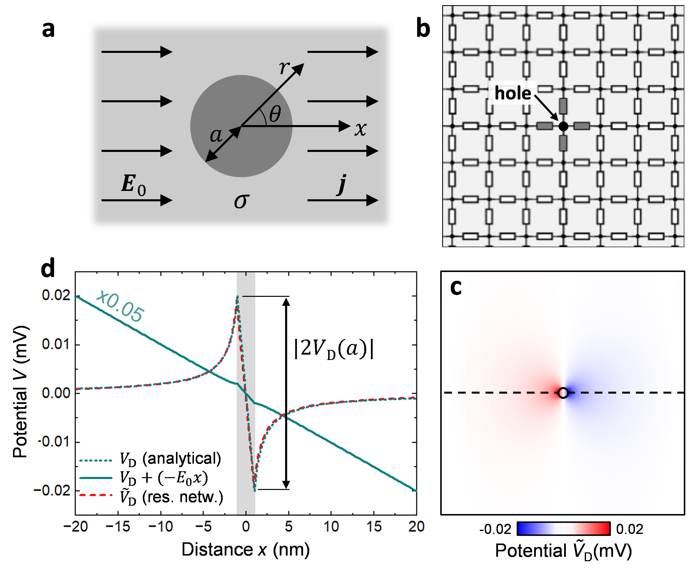
The scattering of charge carriers from a circular defect (such as a hole) of radius in a plane of conductivity (modeled as a two-dimensional electron gas, 2DEG), through which a current is driven in the direction (see Fig. 1a), results in a transport dipole moment . This dipole moment generates a potentialJackson (2021)
| (1) |
in the plane around the defect, in addition to the externally applied potential that drives the current in the first place. Here, is the angle with respect to the current direction and is the distance to the center of the defect. In the diffusive limit , where is the mean free path of the carriers, the dipole moment can be calculated by solving the Laplace equation for the potential in the plane in which the current density spreads out (the conductivity in the defect is assumed to be zero). Since there are no sources and drains in the area of interest (the current is injected and extracted far away from the defect), the normal component of the current density at the defect boundary must be zero, while the potential (and thus also its tangential gradient ) must be continuous. With these boundary conditions, the transport dipole moment in the diffusive limit becomes Jackson (2021)
| (2) |
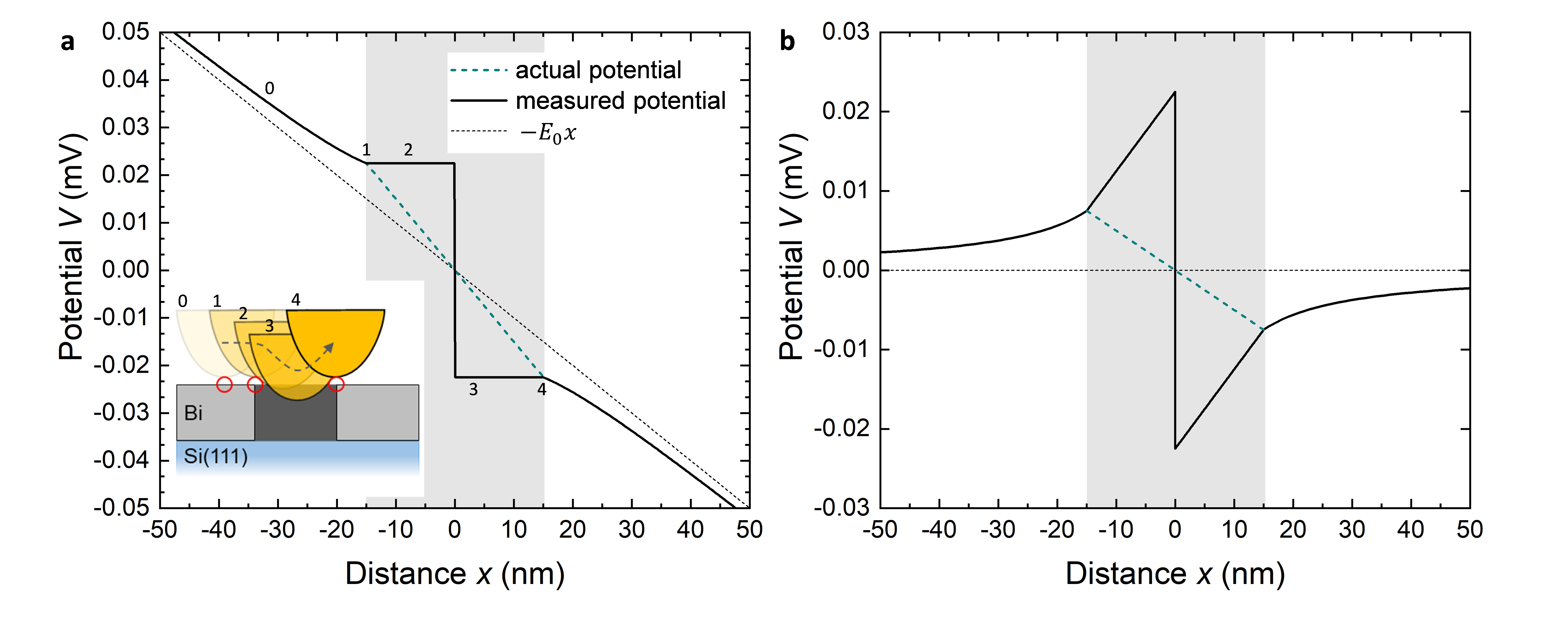
i.e, it scales linearly with the area of the defect and the driving electric field. Inserting into Eq. 1 results in a potential around the defect which reaches at the edges of the defect (Fig. 1)d. The origin of the dipole is the accumulation of carriers in front of and the depletion behind the defect, which in turn has two consequences: Inside the defect, the electric field is constant and twice as large as (potential ), while outside the defect, a local electric field arises that is opposite to the driving field . Thus, the (diffusive) current around the defect is reduced, leading to an increase in resistance in its vicinity. As Fig. 1b-c shows, the resistivity dipole in the diffusive regime can be calculated in the model of a resistor network Cuma (2023), in excellent agreement with the analytical solution in Eqs. 1 and 2.
As defects become smaller, the diffusive resistivity dipole is expected to decrease (Eq. 2). However, once the defect size approaches the carrier mean free path, the model of diffusive transport reaches its limits. Finally, when , the defect interacts with ballistically (rather than diffusively) moving carriers. In this limit, the quasi-Fermi level (electrochemical potential) of right-moving carriers changes sharply (almost discontinuously) across the defect Datta (1997), which now acts as a point scatterer. Since the quasi-Fermi level is a measure of the number of carriers per unit area (carrier density ), the latter also drops sharply at the scatterer, creating an electrostatic potential across the defect. Due to the finite screening length in the 2DEG, the bottom of the band, which in principle must follow the electrostatic potential, cannot follow it on the short length scale . In front of (behind) the defect an accumulation (depletion) of carriers thus occurs, creating the famous Landauer dipole (far away from the defect the carrier concentration equilibrates to a common value) Landauer (1957). To estimate the size of , we observe that it must scale with the scattering cross section, which can be approximated by the transverse linear extension of the defect. At the same time, (as a transport dipole) should to lowest order also scale linearly with the driving field , i.e., . The different scaling behavior of diffusive and Landauer dipoles with defect size implies that at a certain threshold size , the function must cross (with for ). We can expect that . Equating , we find and thus . Inserting and using the conductivity and the carrier density of a 2DEG, we obtain . A more detailed analysis Sorbello and Chu (1988) reveals and thus
| (3) |
where is the Fermi vector.
Analyzing the dipole potential (Eq. 1) at the edges of defects () parallel to the current direction (, we expect from Eqs. 2 and 3 distinct dependencies on the defect sizeFeenstra and Briner (1998): but . Thus, it should be possible to observe the different transport regimes in one and the same sample, as long as it contains defects of different sizes. In such a sample, the defect size can be used as an externally defined length scale on which the scattering behavior in the conducting film, and in particular the transport dipoles, can be observed. We realized this scenario by depositing four monolayers (4 ML) of Bi on a Si(111)- substrate (see Methods section for details). The resulting Bi thin films have a (012) surface orientation and are in the black-phosphorus phase (inset in Fig. 2b), showing large atomically flat terraces (gray in Fig. 2a) with naturally occurring holes (dark) and a small number of adislands (bright) Nagao et al. (2005); Yaginuma et al. (2007). A histogram of the STM topography is displayed in Fig. 2b, showing a dominant peak at 4 ML, and less pronounced peaks for 5, 6, and 8 ML above the background, which stems from the island step edges and the inside of the holes. The holes are irregularly shaped and their sizes vary from to 50 nm (Fig. 2a). For the STP measurements we used our home-built multi-tip scanning tunneling microscope, which allows to analyze the freshly prepared sample under UHV conditions Lüpke et al. (2015, 2017); Voigtländer et al. (2018); Lüpke (2018). This is critical because standard lithography and transport methods are not compatible with the air-sensitive Bi films. To pass a current through the film, we brought two tips into contact with the sample surface and applied a voltage between them (Fig. 2c,d). We then used a third tip in tunneling contact, positioned between source and drain, to map the electrochemical potential (see Methods section for details).
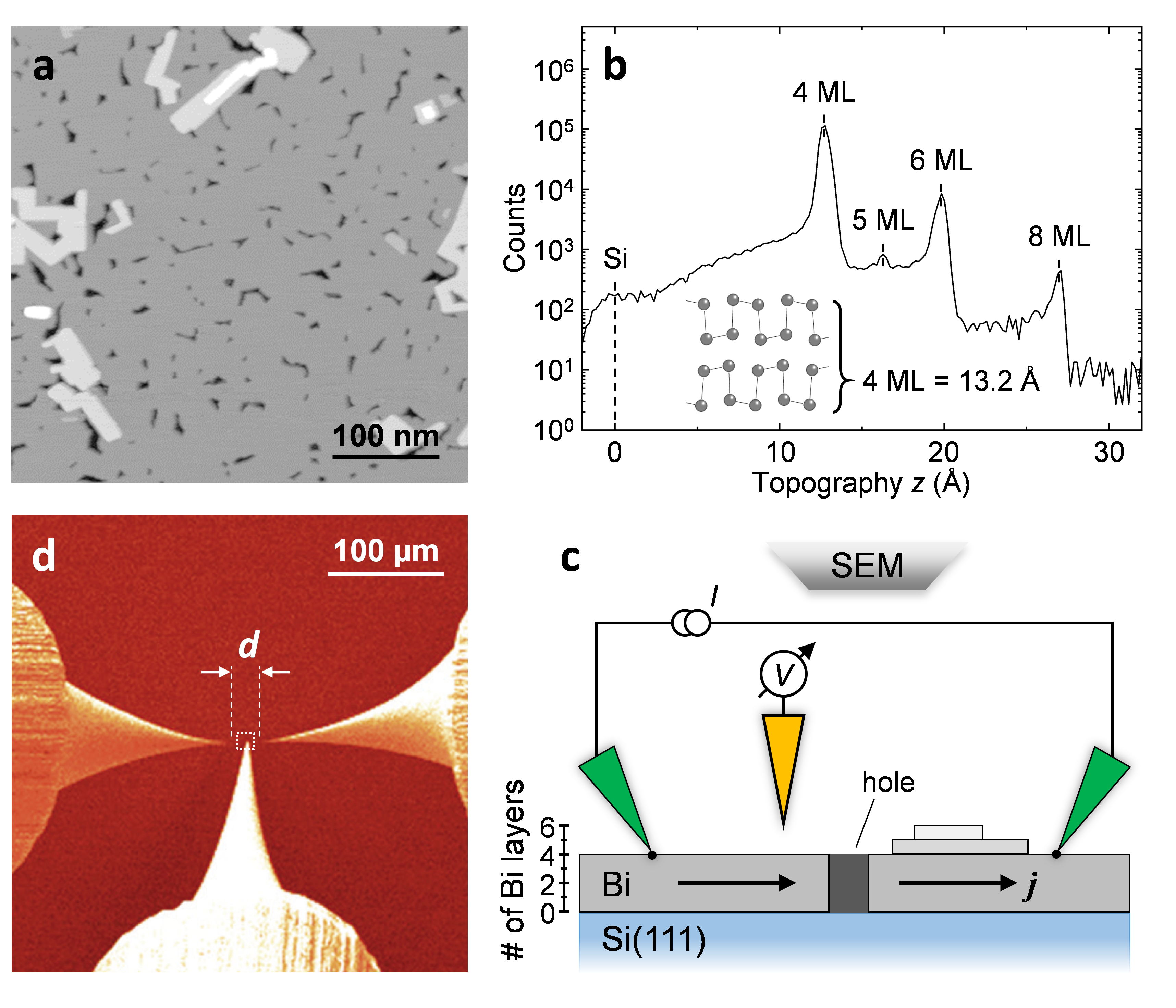
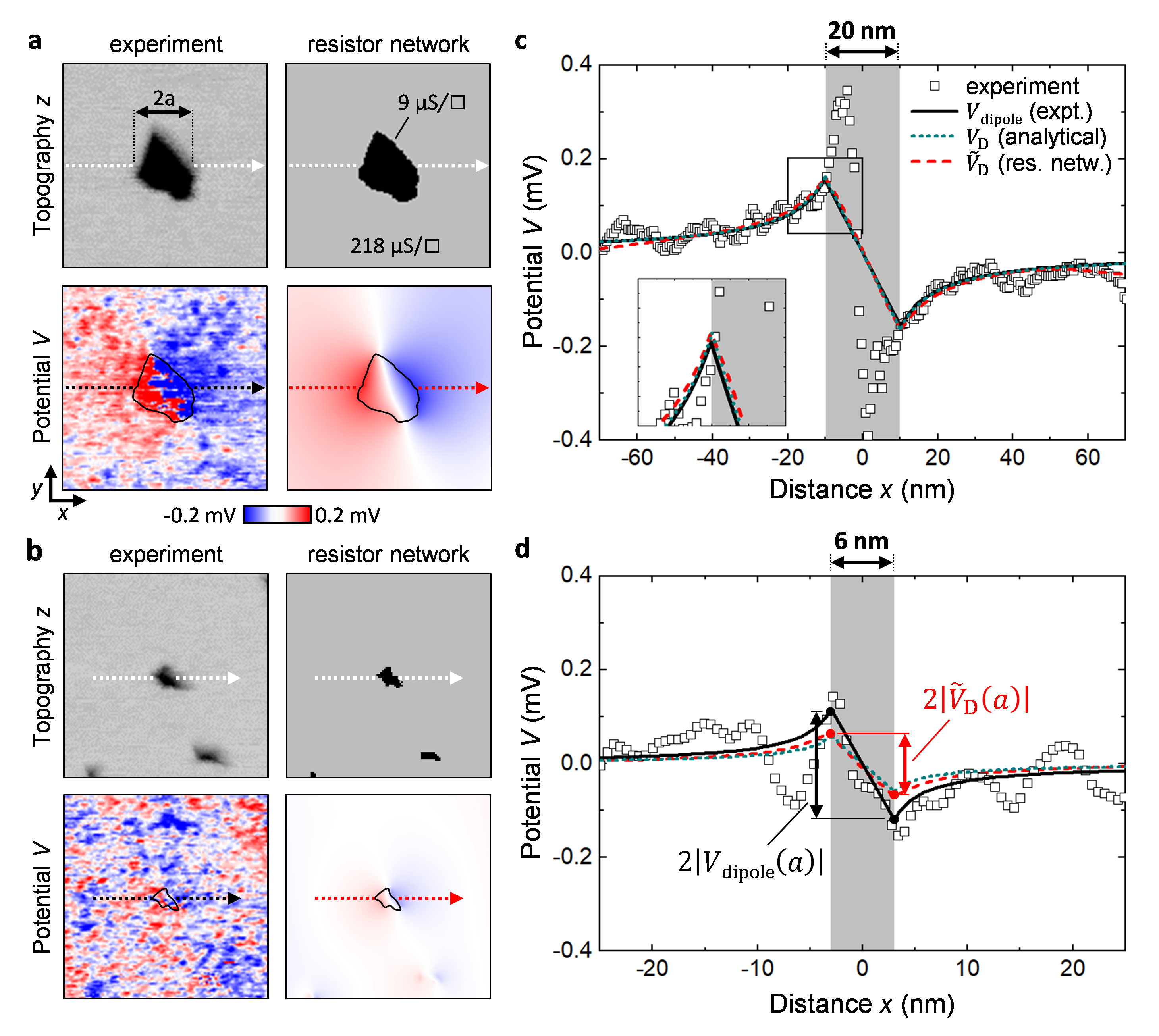
Figure 3a,b shows the measured potential maps (after linear background subtraction, compare Fig. 1) of two exemplary holes, one large ( nm) and one small ( nm). For the purpose of determining the size of the holes, we used a standard threshold detection algorithm (see Methods section for details), resulting in the hole maps shown to the right of the experimental topography images in Figs. 3a,b. We then identified the hole size as half of the extension of hole map in the cross sections, corresponding to the gray shaded areas in Fig. 3c,d. To analyze the dipoles associated with each of the holes, we plotted cross sections of the potential maps parallel to the axis and through the center of the holes () (squares in Figs. 3c,d) and fitted Eq. 1 to the measured potential on the flat Bi film outside the holes, because inside the holes measurement artifacts are present (see Refs. Pelz and Koch, 1990; Cuma, 2023 and the Methods section). This yielded the solid black curves in Fig. 3c,d. Next, we used the hole sizes from the threshold detection algorithm to calculate the analytical diffusive dipole potential (Eqs. 1 and 2), which we then compared to the experimental data as represented by the fitted . For the large hole we see an excellent agreement between (blue dotted curve) and (Fig. 3c). For the small hole, however, is significantly smaller than (Fig. 3b). While this could be an indication that the resistivity dipole at this hole cannot be described by diffusive transport theory, we note that the analytical description of the diffusive dipole () considers a circular hole. The discrepancy between and could therefore also be a consequence of the hole shape.
To account for the influence of the hole shapes on the observed dipoles, we performed resistor network calculations, which allowed us to determine the diffusive resistivity dipole around arbitrarily shaped defects Lüpke et al. (2017); Homoth et al. (2009); Lüpke (2018). For the resistor network calculations we used the same hole maps as before, resulting from the threshold detection algorithm mentioned above. We set the sheet conductivity inside the hole to that of the Si substrate µ (Ref. Just et al., 2015), while for the Bi film we determined the sheet conductivity from the transport field , which yielded µ (see Methods section for more details). The potential maps resulting from the resistor network calculations can be directly compared with the experimental potentiometry data (bottom row of images in Fig. 3a,b). For the cross section of the large hole, we found that our resistor network calculation is in excellent agreement with both the experiment and the analytically determined diffusive dipole (Fig. 3c), confirming that the transport around this defect can be described by the diffusive transport theory. In contrast, for the small hole, the resistor network calculation yielded a larger dipole than predicted by the analytical solution for a circular hole in the diffusive regime (difference between the dashed red and dotted blue curves in Fig. 3d). However, the calculated dipole is still significantly smaller than what was observed experimentally (solid black curve), confirming the discrepancies between experiment and predictions based on diffusive transport theory, no matter whether the latter are based on analytical or resistor network calculations.
To check whether this deviation is systematic, we evaluated the resistivity dipoles of 19 different holes of widely different sizes. For the purpose of comparing experimental resistivity dipoles with the ones resulting from the resistor network calculation, we defined the corresponding dipole potentials as the averages of the positive and negative values at the opposite hole boundaries , as indicated in Fig. 3c,d: . In the inset of Fig. 4 we have plotted the resulting experimental dipoles against the corresponding diffusive dipoles from the resistor network calculations. We find that dipoles mV fall on a line of slope 1, as expected for diffusive transport. In contrast, smaller defects show systematically larger dipoles .
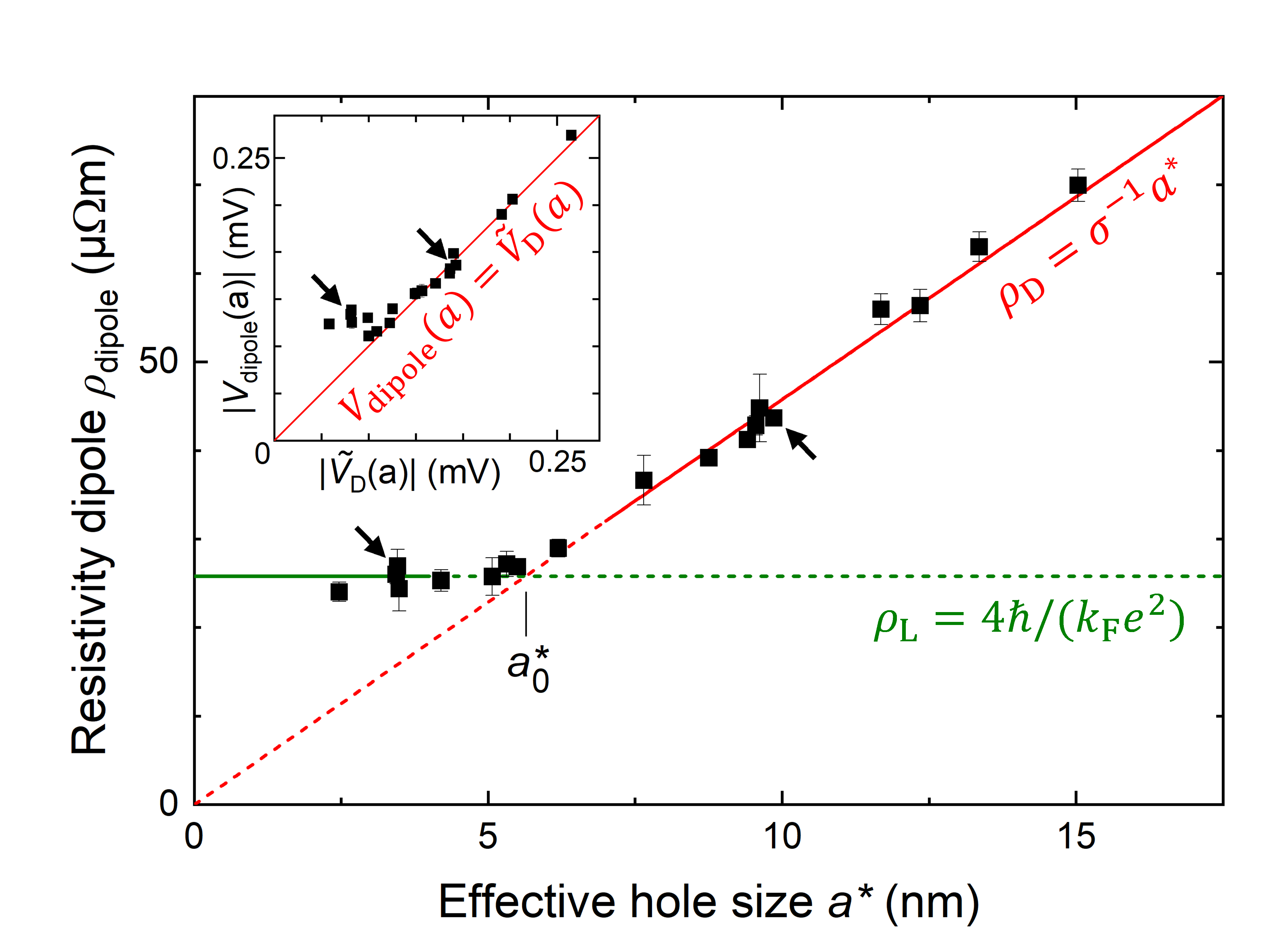
For a quantitative analysis, we need to account for variations in current density between different measurements. To compensate for this, we divided the observed by the current density, resulting in the resistivity dipole . At the same time, we converted as calculated by the resistor network to an effective hole size . The result is shown in the main panel of Fig. 4. For nm the data points clearly show a linear behavior, following , which proves that the scattering at defects of this size can be described by diffusive transport theory. In contrast, for nm, the resistivity dipoles are above the diffusive slope and tend towards a constant resistivity dipole µ. This constant resistivity is a key signature of the Landauer dipole, confirming that defects of this size indeed scatter ballistic carriers. By fitting the constant resistivity of the Landauer dipole (Eqs. 1 and 3), we extracted the Fermi wave vector in the Bi film to be . This value is in agreement with photoemission measurements of corresponding Bi films, which indicate to (Ref. Bian et al., 2014), although theoretical calculations predict a larger nm-1 (Ref. Yaginuma et al., 2007; Bian et al., 2014; Lu et al., 2015). This discrepancy between theory and experiment is most likely caused by a combination of hole doping and disorder, both of which may originate from substrate interactions. Finally, from the hole size at which the transition between the diffusive and ballistic regimes occurs, we estimate a mean free path of . This value is in the range of to reported in the literature for Bi films on Si(111)- Feenstra and Briner (1998); Hirahara et al. (2007); Briner et al. (1996). We further note that the theoretical conductivity of the 2DEG in the Drude model is (Ref. Datta, 1997), where we used the values for and extracted from our analysis. This result is in excellent agreement with our experimental sheet conductivity of , confirming the correctness of the diffusive dipole slope in Fig. 4 and, more generally, corroborating the consistency of our analysis.
In conclusion, we have provided compelling evidence for the transition between diffusive and ballistic resistivity dipoles around defects in ultra-thin Bi films as a function of defect size. The moderate mean free paths in our samples proved amenable to identifying defects in both limits, allowing us to unambiguously pinpoint the transition and consistently extract crucial material parameters of our Bi films: the sheet conductivity from the slope of the diffusive resistivity dipole as function of the hole size, the mean free path from the defect size at which the transition to the ballistic scattering regime occurs, and the Fermi wave vector from the saturation value of the Landauer residual resistivity dipole at small defect size. Notably, our resistor network calculations take into account the significant influence of the irregular defect shapes in the diffusive regime, allowing us to exclude the latter as a source of the observed deviations from the analytical solution for circular holes. We foresee that the particularly clear picture of the resistivity dipoles as reported here, obtained by combining in situ growth of Bi films on Si(111)- with scanning tunneling potentiometry in ultra-high vacuum, will facilitate further investigations in at least two directions: First, because a decrease in temperature will shift the transition between the diffusive and ballistic regimes to larger defects, a detailed study of temperature-dependent transport (including means free paths) will become possible. Such low-temperature STP experiments also promise to resolve the transition in even more detail, because of further improvements in experimental resolution Lüpke et al. (2015) and access to more detailed information of the Fermi surface Wexler (1966); Allen (2006); Popov and Gorbunov (1963). Second, our clear identification scheme of the ballistic regime will greatly benefit the search for current-induced oscillations in the carrier density Zwerger et al. (1991); Kramer (2012), which are expected around defects in addition to the Landauer resistivity dipole and the well-known (and often observed) Friedel oscillations at zero current Friedel (1954). It is interesting to note that already our potentiometry measurement in Fig. 3d shows conspicuous oscillations, the nature of which is currently unclear and therefore requires further study.
I Methods
I.1 Sample preparation
An 8 4 mm2 piece of Si(111) (miscut , ) was degassed under ultra-high vacuum (UHV) conditions at for several hours, followed by repeated flash-annealing cycles at for 30 s each. After flashing, the sample was first quenched to , followed by cooling to at a relatively slow rate of . The sample was then quenched a second time, this time to and held at this temperature for 30 min to form a well ordered Si(111)- surface structure, followed by a final quench to room temperature. During sample preparation, the direction of the heating current (technical current direction) was in the ”step-up” direction, so that the resulting Si(111)- surface showed parallel step bunches with several hundred nanometer wide flat terraces in between Gibbons (2006); Romanyuk (2009). 4 ML of Bi were deposited on the Si(111)- surface at room temperature from a Knudsen effusion cell at a deposition rate of , where (Ref. Nagao et al., 2005).
I.2 Scanning tunneling potentiometry
After preparation, the sample was transferred to the room-temperature multi-tip STM equipped with electrochemically etched tungsten tips cleaned in situ by resistive heating. The pressure during the measurements was mbar and we did not observe any surface contamination even a few weeks after the measurements. The STP measurements were performed on flat terraces away from step bunches, where the flow of a lateral current is not influenced by any substrate steps. The sample surface was contacted with two tips to inject a lateral current in the range to mA at a tip-to-tip distance of to µ. At this tip distance and given the chosen resistivity of the Si wafer (see above), no significant current is expected to flow through the Si substrate Just et al. (2015). We then used a third tip to simultaneously map the topography and electrochemical potential in the central region between the two current-injecting tips, where the current density is given by , by scanning the tip in tunneling contact using an interrupted feedback technique: The local sample topography and potential at each pixel were determined by alternating measurements with first topography feedback and then potential feedback. For potential feedback, the tip was held at a constant height above the sample while the voltage applied to the tip was adjusted by a software feedback loop until the tunneling current disappeared. The voltage at which this occurred was recorded as the local potential of the sample. The initial tip bias was then restored and the scan continued to the next scan position. The resulting spatial and potential resolution was as low as Å and µV for typical tunneling parameters , . For details on the implementation of this technique, see Refs. Lüpke et al. (2015); Lüpke (2018). Cross sections of the measured potential maps were averaged over a 6 pixel wide stripe.
I.3 Hole detection
To detect the holes, we used a standard threshold detection algorithm on the STM topography data. The latter were acquired simultaneously with the potential data. Due to the finite tip radius in our experiments (which is expected to be large compared to the smallest holes), the edges of the holes are smeared out in the STM topography, requiring a careful choice of the threshold. We found Å below the flat terraces surrounding the holes to be a suitable threshold for detecting the holes. This value was determined by comparing the experimental data with the resistor network calculations of large holes; both must coincide because the latter are deep in the diffusive regime.
We note that the finite tip radii can also lead to an apparent extension of the potential dipole into the holes, because the sharp hole edge makes the tunneling channel move across the surface of the blunt tip. This behavior is observed for example in Fig. 2c, and is schematically explained in Supplemental Fig. S1. The tunneling setpoint current maintains a constant tip-sample distance corresponding to the radius of the red circles in the inset of Fig. S1a. Outside of the hole (tip position 0), the tunneling contact is always between the tip apex and the flat surface (left red circle). However, due to the tip shape, once the tip apex is in the hole the tunneling current still flows from the left edge of the hole (middle red circle) but to different positions on the tip surface (tip positions 1, 2). Beyond the half-way point across the hole (tip position 3), the tunneling contact jumps to the opposite edge of the hole (right red circle), where it remains until the tip is outside the hole again (tip position 4). As a result, the measured potential within the hole is determined by the tip shape and the potential at the hole edges. In detail, as the tip enters the hole from the left, a constant potential corresponding to the potential at the left hole edge is measured for a certain range of values into the hole, until a sudden jump to a second constant value corresponding to the potential at the right hole edge occurs, which in turn continues until the tip exits the hole. After subtracting the linear background (Fig. S1b), the measured potential inside the hole shows an upward slope which is opposite to the actual potential inside the hole (dashed blue line), disrupted by a sharp step where the tunneling contact jumps from the left to the right hole edge. It is important to note, however, that the effect of the finite tip radius does not play a role in the determination of , which exclusively takes into account the potential measured on the flat surface outside of the holes.
I.4 Resistor network calculation
Resistor network calculations were implemented on a square lattice where neighboring nodes are connected by resistors. The resistance value of each resistor corresponded to either the Bi-film conductivity or, inside the holes, the Si(111)--substrate conductivity; the corresponding conductances between neighboring nodes were entered into a conductivity matrix . We then imposed a current between the left and right boundaries of the system and used Kirchhoff’s current law to numerically solve the linear system of equations for the potential distribution . We plot the resulting potential distribution as images in which each pixel corresponds to one node. Such model simulations accurately reproduce diffusive transport around a defect when the node-to-node distance is significantly smaller than the mean free path of the charge carriers (Fig. 1). Further details can be found in Refs. Lüpke, 2018; Cuma, 2023.
References
- Landauer (1957) R. Landauer, IBM J. Res. Dev. 1, 223 (1957).
- Feenstra and Briner (1998) R. Feenstra and B. Briner, Superlattices Microstruct. 23, 699 (1998).
- Lüpke et al. (2017) F. Lüpke, M. Eschbach, T. Heider, M. Lanius, P. Schüffelgen, D. Rosenbach, N. von den Driesch, V. Cherepanov, G. Mussler, L. Plucinski, D. Grützmacher, C. M. Schneider, and B. Voigtländer, Nat. Commun. 8 (2017).
- Muralt and Pohl (1986) P. Muralt and D. Pohl, Appl. Phys. Lett. 48, 514 (1986).
- Briner et al. (1996) B. G. Briner, R. M. Feenstra, T. P. Chin, and J. M. Woodall, Phys. Rev. B 54, R5283 (1996).
- Bannani et al. (2008) A. Bannani, C. Bobisch, and R. Möller, Rev. Sci. Instrum. 79 (2008).
- Lüpke et al. (2015) F. Lüpke, S. Korte, V. Cherepanov, and B. Voigtländer, Rev. Sci. Instrum. 86, 123701 (2015).
- Lüpke (2018) F. Lüpke, Scanning tunneling potentiometry at nanoscale defects in thin films, Ph.D. thesis, RWTH Aachen University (2018).
- Ji et al. (2012) S.-H. Ji, J. B. Hannon, R. Tromp, V. Perebeinos, J. Tersoff, and F. M. Ross, Nat. Mater. 11, 114 (2012).
- Willke et al. (2015) P. Willke, T. Druga, R. G. Ulbrich, M. A. Schneider, and M. Wenderoth, Nat. Commun. 6, 6399 (2015).
- Willke et al. (2017) P. Willke, T. Kotzott, T. Pruschke, and M. Wenderoth, Nat. Commun. 8, 15283 (2017).
- Momeni Pakdehi et al. (2018) D. Momeni Pakdehi, J. Aprojanz, A. Sinterhauf, K. Pierz, M. Kruskopf, P. Willke, J. Baringhaus, J. Stöckmann, G. Traeger, F. Hohls, C. Tegenkamp, M. Wenderoth, F. Ahlers, and H. Schumacher, ACS Appl. Mater. Interfaces 10, 6039 (2018).
- Mogi et al. (2019) H. Mogi, T. Bamba, M. Murakami, Y. Kawashima, M. Yoshimura, A. Taninaka, S. Yoshida, O. Takeuchi, H. Oigawa, and H. Shigekawa, ACS Appl. Electron. Mater. 1, 1762 (2019).
- Sinterhauf et al. (2021) A. Sinterhauf, G. A. Traeger, D. Momeni, K. Pierz, H. W. Schumacher, and M. Wenderoth, Carbon 184, 463 (2021).
- Krebs et al. (2023) Z. J. Krebs, W. A. Behn, S. Li, K. J. Smith, K. Watanabe, T. Taniguchi, A. Levchenko, and V. W. Brar, Science 379, 671 (2023).
- Krebs et al. (2024) Z. J. Krebs, W. A. Behn, K. J. Smith, M. A. Fortman, K. Watanabe, T. Taniguchi, P. S. Parashar, M. M. Fogler, and V. W. Brar, arXiv preprint arXiv:2409.19468 (2024).
- Bauer and Bobisch (2016) S. Bauer and C. A. Bobisch, Nat. Commun. 7, 11381 (2016).
- Geng et al. (2016) H. Geng, W.-Y. Deng, Y.-J. Ren, L. Sheng, and D.-Y. Xing, Chin. Phys. B 25, 097201 (2016).
- Morr (2016) D. K. Morr, Contemp. Phys. 57, 19 (2016).
- Cherepanov et al. (2012) V. Cherepanov, E. Zubkov, H. Junker, S. Korte, M. Blab, P. Coenen, and B. Voigtländer, Rev. Sci. Instrum. 83 (2012).
- Voigtländer et al. (2018) B. Voigtländer, V. Cherepanov, S. Korte, A. Leis, D. Cuma, S. Just, and F. Lüpke, Rev. Sci. Instrum. 89 (2018).
- Jackson (2021) J. Jackson, Classical Electrodynamics (Wiley, 2021).
- Cuma (2023) D. Cuma, Multi-tip scanning tunneling potentiometry on thin bismuth films and topological insulators in a cryogenic system, Ph.D. thesis, RWTH Aachen University (2023).
- Datta (1997) S. Datta, Electronic Transport in Mesoscopic Systems (Cambridge University Press, 1997).
- Sorbello and Chu (1988) R. S. Sorbello and C. S. Chu, IBM J. Res. Dev. 32, 58 (1988).
- Nagao et al. (2005) T. Nagao, S. Yaginuma, M. Saito, T. Kogure, J. Sadowski, T. Ohno, S. Hasegawa, and T. Sakurai, Surf. Sci. 590, 247 (2005).
- Yaginuma et al. (2007) S. Yaginuma, T. Nagao, J. Sadowski, M. Saito, K. Nagaoka, Y. Fujikawa, T. Sakurai, and T. Nakayama, Surf. Sci. 601, 3593 (2007).
- Pelz and Koch (1990) J. Pelz and R. Koch, Rhys. Rev. B 41, 1212 (1990).
- Homoth et al. (2009) J. Homoth, M. Wenderoth, T. Druga, L. Winking, R. G. Ulbrich, C. A. Bobisch, B. Weyers, A. Bannani, E. Zubkov, A. M. Bernhart, M. R. Kaspers, and R. Möller, Nano Lett. 9, 1588 (2009).
- Just et al. (2015) S. Just, M. Blab, S. Korte, V. Cherepanov, H. Soltner, and B. Voigtländer, Rhys. Rev. Lett. 115, 066801 (2015).
- Bian et al. (2014) G. Bian, X. Wang, T. Miller, T.-C. Chiang, P. J. Kowalczyk, O. Mahapatra, and S. Brown, Rhys. Rev. B 90, 195409 (2014).
- Lu et al. (2015) Y. Lu, W. Xu, M. Zeng, G. Yao, L. Shen, M. Yang, Z. Luo, F. Pan, K. Wu, T. Das, P. He, J. Jiang, J. Martin, Y. Ping Feng, H. Lin, and X.-s. Wang, Nano Lett. 15, 80 (2015).
- Hirahara et al. (2007) T. Hirahara, I. Matsuda, S. Yamazaki, N. Miyata, S. Hasegawa, and T. Nagao, Appl. Phys. Lett. 91, 202106 (2007).
- Wexler (1966) G. Wexler, Proc. Phys. Soc. 89, 927 (1966).
- Allen (2006) P. Allen, Conceptual Foundations of Materials (Elsevier, 2006) pp. 165–218.
- Popov and Gorbunov (1963) V. Popov and V. Gorbunov, Sov. Phys. J 16, 517 (1963).
- Zwerger et al. (1991) W. Zwerger, L. Bönig, and K. Schönhammer, Rhys. Rev. B 43, 6434 (1991).
- Kramer (2012) B. Kramer, Quantum transport in semiconductor submicron structures (Springer Science & Business Media, 2012).
- Friedel (1954) J. Friedel, Adv. Phys. 3, 446 (1954).
- Gibbons (2006) B. J. Gibbons, Electromigration induced step instabilities on silicon surfaces, Ph.D. thesis, The Ohio State University (2006).
- Romanyuk (2009) K. Romanyuk, Influence of the step properties on submonolayer growth of Ge and Si at the Si(111) surface, Ph.D. thesis, RWTH Aachen University (2009).