Consequences of magneto-electrical coupling in multiferroic VSe2Sc2CO2 heterostructures.
Abstract
Two-dimensional van der Waals heterostructures are potential game changers both in understanding the fundamental physics and in the realization of various devices that exploit magnetism at the nanoscale. Multiferroic heterostructures comprising a two-dimensional ferroelectric and a two-dimensional ferromagnet are ideal candidates for electrical control of properties of the ferromagnets that can lead to non-volatile memory devices, for example. Relatively new but immensely promising two-dimensional materials, MXene and transition metal dichalcogenides, can be effectively combined to achieve the goal as both have flexibilities in their structures and compositions that are tunable. In this work, using Density Functional Theory, we have investigated the magneto-electric coupling driven transitions in the electronic ground states of VSe2-Sc2CO2 bi-layer and tri-layer heterostructures. Our results demonstrate that the change in the ferroelectric polarisation in the MXene layer leads to changes in the spin-polarized band structures of the magnetic component VSe2 enabling a semiconductor to half-metal transition in these heterostructures. We propose several applications of this magneto-electric coupling in these multiferroic heterostructures that can lead to the efficient operation of Field Effect transistors and achieve non-volatility in memory devices at the nanoscale.
I Introduction
Lately, electronic devices for information and communications are in high demand as the storage of huge amounts of data and faster communication are the keys to success in an era of data-driven science and technology. Non-volatility of the hardware components is one basic requirement in this scheme so that a large cache of data can be retained every time the device is disconnected from the power supply [1]. With the advent of storage and various electrical devices that exploit the science of magnetism, remarkable advances have been possible in this direction [2, 3, 4, 5, 6, 7, 8]. At the same time, demand for miniaturization of the devices has led to the exploration of materials for devices in low dimensions. The discovery of magnetism in two-dimensions (2D) [9, 10, 11, 12, 13, 14] has given a substantial boost towards the realization of miniaturized magnetic storage and various electrical devices. At the heart of this is the electrical control of atomic-thick Ferromagnetism, in particular. The idea has been explored in cases of prototype 2D magnets like CrI3 [15, 16, 17], Cr2Ge2Te6 [18] and Fe2GeTe2 [19, 20]. Though promising, exploring them as non-volatile memory or storage devices is bound to fail as they require continuous electrical control for the sustenance of the states induced by electrical switching.
The non-volatile electrical control of magnetic devices can be realized in multiferroic materials where the magnetism is controlled by the Ferroelectric polarization. Since Ferroelectric materials are endowed with bi-stable polarized states, their electrical switching is completely non-volatile. Thus, if the magnetic properties can be coupled with the states of electric polarization, the resulting magneto-electric coupling will lead to non-volatile electrical control of magnetic states [21, 22, 23]. However, single-phase multiferroics are not very attractive for applications as none of the existing materials combine large and robust electric and magnetic polarizations at room temperature [24]. This has been circumvented by forming two-phase composites with a Ferroelectric and a Ferromagnetic component. The magneto-electric effect is significant if the coupling at the interface of the two is large. This is more effective if the area at the interface is large.
Making 2D Van der Waals (vdW) heterostructures with a 2D Ferroelectric and a 2D ferromagnet, thus, can be a useful way to achieve this. With the synthesis of several 2D Ferroelectrics [25, 26, 27, 28, 29, 30], construction of such heterostructures no longer remains a distant reality. Very recently, this idea has been demonstrated to be working as a proof of concept through Density Functional Theory [31] based calculations [32, 33, 34, 35, 36, 37]. In those calculations, MXene Sc2CO2, recently predicted to be possessing large out-of-plane Ferroelectric polarization [38] from DFT calculations, is considered to be the Ferroelectric component in the 2D heterostructure. Different 2D Ferromagnets having minimal lattice mismatch with Sc2CO2 have been used as the magnetic component. The calculations showed that the electronic ground states of the heterostructure can be altered between semiconducting and half-metallic upon changes in the Ferroelectric polarization. Taking a cue from these recent developments, in this work, we have explored the consequences of magneto-electrical coupling in bi-layer and tri-layer VSe2/Sc2CO2 heterostructures. The transition-metal dichalcogenide(TMDC)-MXene heterostructures have been considered as both have flexibilities in their compositions and structures that can be exploited to realize tunable functional properties. As the magnetic component of the heterostructures, we have considered the 2H phase of VSe2 as its monolayer has been synthesized recently [39]. Our results show that the electronic ground states of these heterostructures can be reversibly switched between semiconducting and half-metallic states upon switching electrical polarization of Sc2CO2. Based on these findings, we propose these heterostructures for multiple applications like bi-polar magnetic semiconductors, tunneling field effect transistors, and low-cost, power-efficient non-volatile memory devices.
II Computation Details
All calculations in this work are performed using Density Functional Theory (DFT)[31] as implemented in Vienna ab initio simulation package (VASP) [40]. The electron-ion interactions are described using projector augmented wave (PAW) basis set [41]. The exchange-correlation part of the Hamiltonian is approximated by generalized gradient approximation (GGA) as parameterized by Perdew-Burke-Ernzerhof (PBE) [42]. The kinetic energy cutoff of the plane wave is set to be 600 eV. The energy and force cutoff for structural optimization are eV and 0.01 eV/Å, respectively. To include the van-der-Waals interactions, the DFT-D3 method is employed [43]. The Brillouin zone is sampled using Monkhorst-Pack [44] -point mesh. Dipole corrections are also taken into account in all the calculations. A 20 Åvacuum is considered along -direction to avoid any interactions between the adjacent layers.
III RESULTS AND DISCUSSIONS
III.1 Ferroelectric polarisation driven modifications in the electronic properties of VSe2/Sc2CO2
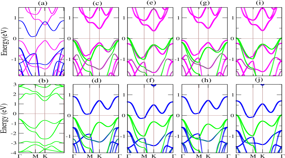
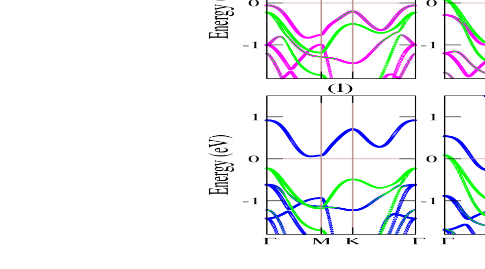
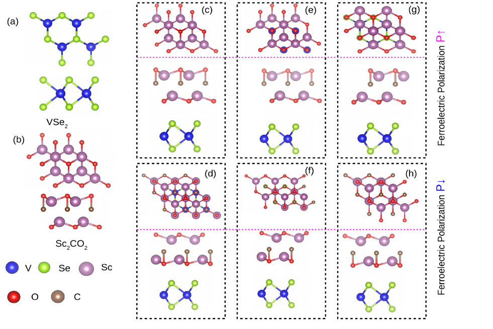
Figure 1(a) presents the top and side views of monolayer 2H-VSe2, the magnetic component of the heterostructure. It crystallizes in a honeycomb-like structure where each V(Se)-atom is surrounded by six(three) neighboring Se(V) atoms. The V atoms are in a trigonal prismatic crystal field formed by the surrounding ligands. This VSe2 phase exhibits ferromagnetism with a very high Curie temperature of 425 K [45]. Due to its high transition temperature, it can be directly used for applications above room temperature. The lattice constant of VSe2 from our calculation is 3.33 Å, which agrees very well with the reported result [46]. The magnetic moment of each V atom is 1 .
The ground state structure of MXene monolayer Sc2CO2, the ferroelectric component of the heterostructure, is shown in Figure 1(b). Monolayer Sc2CO2 possesses out-of-plane ferroelectricity with significantly large electric polarisation [38]. The structure lacks inversion symmetry. The O-atom on one of the surfaces occupies the hollow site associated with the Sc atom. The O-atom, on the other surface, occupies the hollow site associated with the C-atom. Consequently, the Sc atom on the lower surface (00-1 surface) is in an octahedral crystal field, while the Sc atom on the top surface (001 surface) is in a trigonal prismatic crystal field. The lattice parameter for Sc2CO2 from our calculations is 3.41 Å, in excellent agreement with the reported results [35, 47].
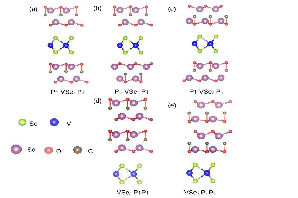
Our result demonstrates that the lattice mismatch between VSe2 and Sc2CO2 is nearly 2.4 % only. Hence, these two monolayers can be vertically stacked to form a 2D van der Waals (vdW) heterostructure. The two ferroelectric polarization states of Sc2CO2 are differentiated by the position of the C atom in the unit cell. When the C atom is close to the upper(lower) surface, the polarisation state is depicted as P(P). These two polarisation states can be reversibly switched by applying an electric field and occur through an intermediate antiferroelectric structure [38]. The heterostructure with VSe2 can be formed with either state of ferroelectric polarisation. Accordingly, we construct six different heterostructures, three each for a given ferroelectric polarisation: (i) AA: The O-atom closest to VSe2 is directly above the V-atom (Figure 1(c),(d)) (ii) BB: The O-atom closest to VSe2 is directly above the Se atom (Figure 1(e),(f)) and (iii) CC: The O-atom closest to VSe2 is above a V-Se bond in VSe2 (Figure 1(g),h)).
| Stacking | d (Å) | Eb (meV/Å2) | Band Gap(eV) |
| AA-P | 2.90 | -19.84 | 0.12 |
| AA-P | 2.81 | -31.50 | 0.00 |
| BB-P | 3.4 | -13.27 | 0.16 |
| BB-P | 3.35 | -17.5 | 0.00 |
| CC-P | 3.02 | -17.8 | 0.12 |
| CC-P | 2.93 | -31.4 | 0.00 |
The stability of the six heterostructures is assessed by calculating their binding energies given by
is the total energy of the heterostructure. and are the energies of pristine monolayers of VSe2 and Sc2CO2, respectively . is the surface area of the heterostructure. The results are presented in Table 1. The results imply that the heterostructures can be grown experimentally. The interlayer distance in each case is also given in Table 1. We find that the interlayer distances decrease when the ferroelectric polarisation of Sc2CO2 changes from P to P. For a given structural configuration, the maximum changes in the interlayer distances are about 3% only upon a change in the state of ferroelectric polarisation.
We next investigate the magneto-electric coupling in the bi-layer VSe2-Sc2CO2 by computations of band structures of the heterostructures considered in this work. In Figure 2(a) and 2(b), we show the band structures of monolayer VSe2 and Sc2CO2, respectively. VSe2 turns out to be a ferromagnetic semiconductor with a band gap of 0.75 eV(0.53 eV) in the spin-up(spin-down) channel, in agreement with existing results [46]. Our calculations show Sc2CO2 a semiconductor with an indirect band gap of 1.84 eV, in excellent agreement with other calculations[32]. The spin-projected band structures of bi-layer VSe2/Sc2CO2 for different heterostructures and different ferroelectric polarisations are shown in Figure 2(c)-(n). A common feature seen in all cases is that the band structure of the heterostructures is essentially a superposition of bands contributed by the constituents. This is the characteristic of 2D vdW heterostructures with weak coupling between the layers.
The other common feature connected to the magneto-electrical coupling in this system is the dependence of spin projected band structure on the ferroelectric polarisation of MXene Sc2CO2. In Figure 2 (c) and (d), we show the spin up and spin down bands of the AA heterostructure, respectively, when the ferroelectric polarisation is P. We find that the system behaves as a magnetic semiconductor with a band gap of 0.12 eV (Table 1). Here, both the valence band minima (VBM) and conduction band maxima (CBM) are due to contributions from VSe2, demonstrating a type-I band alignment. Such heterostructures with type-I band alignment are useful for confining electrons and holes, facilitating carrier recombination, and thus sought after for applications in optical devices. Significantly, the VBM and the CBM are composed of oppositely polarised spin bands. As such, the heterostructure behaves like a Bipolar Magnetic Semiconductor (BMS). In this system, a completely spin polarisation current with reversible spin polarisation can be created and controlled simply by applying a gate voltage [48]. When the polarisation state of Sc2CO2 ferroelectric is switched to P, the heterostructure behaves as a half-metal (Figure 2 (e),(f)). In the spin-up channel, the system remains semiconducting with little changes in the band structure (Figure 2(e)). Major changes are observed in the spin-down bands (Figure 2(f)). The spin-down band corresponding to VSe2, right above Fermi level in case of both monolayer VSe2 and the heterostructure with P ferroelectric state, is pushed towards lower energy, closing the semiconducting gap, leading to a half-metallic ground state of the heterostructure.
In experiments, switching between the two states, P and P, can be done by applying an electric field. Sc2CO2, being ferroelectric, is bistable. As a result, the application of an electric field can change its polarization state. It remains in a given state of polarisation even after removing the electric field, making the switching completely reversible and non-volatile. Figure 2, therefore, shows that the ground state of Sc2CO2/VSe2 heterostructure can be switched between a magnetic semiconductor and a half-metal by reversible switching of the ferroelectric polarisation.
III.2 Coupling Mechanism and interfacial interaction in VSe2/Sc2CO2 heterostructure
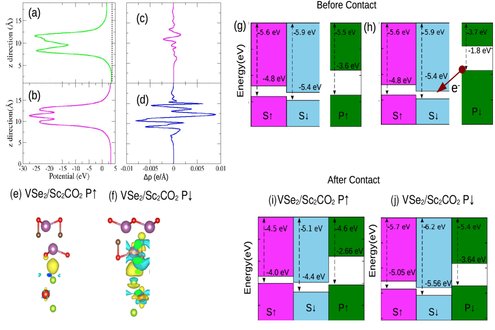
The observed changes in the electronic structures of VSe2/Sc2CO2 upon changing the ferroelectric polarisation state can be understood by analyzing the changes in the charge distribution or coupling across the monolayer interfaces. Due to broken spatial symmetry, the work function associated with two surfaces of Sc2CO2 is different by about 1.8 as seen from the plane-averaged potential versus distance in the -direction plot (Figure 3(a)). No such asymmetry across the surfaces is observed in the case of VSe2 (Figure 3(b)). The calculated Work functions of VSe2 monolayer, the Ctop side and Cbottom side of Sc2CO2 monolayer are -5.46 eV, -4.96 eV and -3.13 eV, respectively; Ctop(Cbottom) refers to the position of C-atom layer in Sc2CO2 when the ferroelectric polarisation is P(P). Thus, when VSe2 is stacked with Sc2CO2, depending on which surface of Sc2CO2 is used for stacking, charge transfer across the interface differs significantly. When Sc2CO2 is in the P polarisation state, the spin-up(S) and spin-down(S) valence band maxima (VBM) (conduction band minima(CBM)) of VSe2 are lower(higher) than the conduction band minima (CBM)(valence band maxima (VBM)) of Sc2CO2 (Figure3(g)). Thus, in VSe2/Sc2CO2(P) heterostructure, there is no electron transfer between Sc2CO2 and VSe2. Nevertheless, due to differences in the work functions of Sc2CO2 and VSe2 the interfacial interaction causes a spontaneous flow of electrons from Sc2CO2 to VSe2. Accordingly, the Fermi level of Sc2CO2 shifts slightly towards lower energy, and that of VSe2 shifts slightly towards higher energy, reaching a common level. As a result, a small amount of electron accumulates in VSe2, giving rise to an internal electric field. The charge transfer, however, is not sufficient to close the energy gap, resulting in a type I band alignment (Figure 3(i)). The variations in the plane-averaged differential charge density with distance along (Figure 3(c)) and charge density difference (Figure 3(e)) results corroborate this.
When the polarization of Sc2CO2 changes to P (Figure 3(h)),the VBM of Sc2CO2is at a higher position than CBM of VSe2 associated with either spin band. Therefore, electron transfer can occur from the valence band of Sc2CO2 to the conduction band of the spin-down channel of VSe2. Due to this, the spin-down conduction band of VSe2 is shifted towards lower energy considerably, closing the semiconducting gap in this spin channel and giving rise to metallic behavior (Figure 3(j)). The band alignment shown in Figure 3(j) indicates that this heterostructure exhibits an almost broken-gap type-III alignment. Heterostructures with such band alignment can facilitate tunneling of electrons directly from the VBM of Sc2CO2 to the CBM of VSe2. Therefore, band-to-band tunneling (BTBT) is possible, making these heterostructures highly desirable for tunnel field-effect transistors. The plane-averaged differential charge density (Figure 3(d)) and charge density difference(Figure 3(f)) plots show a significant amount of charge transfer across the interface justifying the band alignment described above. Such large charge transfer across the interface can be explained in terms of the significant difference in the Work functions of VSe2 and Cbottom side of the Sc2CO2 monolayer.
III.3 Ferroelectric polarisation driven modifications in the electronic properties of Sc2CO2/VSe2/Sc2CO2
| System | Eb |
| Sc2CO2(P)/VSe2/Sc2CO2(P) | -30.00 |
| Sc2CO2(P)/VSe2/Sc2CO2(P) | -21.75 |
| Sc2CO2(P)/VSe2/Sc2CO2(P) | -31.24 |
| VSe2/Sc2CO2(P)Sc2CO2(P) | -29.60 |
| VSe2/Sc2CO2(P)Sc2CO2(P) | -51.95 |
Next, we investigate the interrelations between a number of layers in the VSe2-Sc2CO2 heterostructure, the ferroelectric polarisation, and the ground state electronic structure. For this purpose, we construct a tri-layer Sc2CO2/VSe2/Sc2CO2 heterostructure. Since the AA stacking configuration has the lowest binding energy in the bi-layer heterostructure, and since a different stacking configuration did not produce any qualitatively different result, we have considered only the AA stacking configuration for this trilayer heterostructure. Three different arrangements, (a) Sc2CO2(P)/ VSe2/ Sc2CO2(P) (b)Sc2CO2(P)/ VSe2/ Sc2CO2(P) (c) Sc2CO2(P)/ VSe2/ Sc2CO2(P), are considered. Additionally,two more arrangements, Sc2CO2(P)/Sc2CO2(P)/VSe2 and Sc2CO2(P)/Sc2CO2(P)/VSe2 are considered for the purpose of comparison. The arrangements are shown in Figure 4. Binding energies corresponding to them are given in Table 2. The negative values of binding energies indicate that the heterostructures can form with these arrangements.
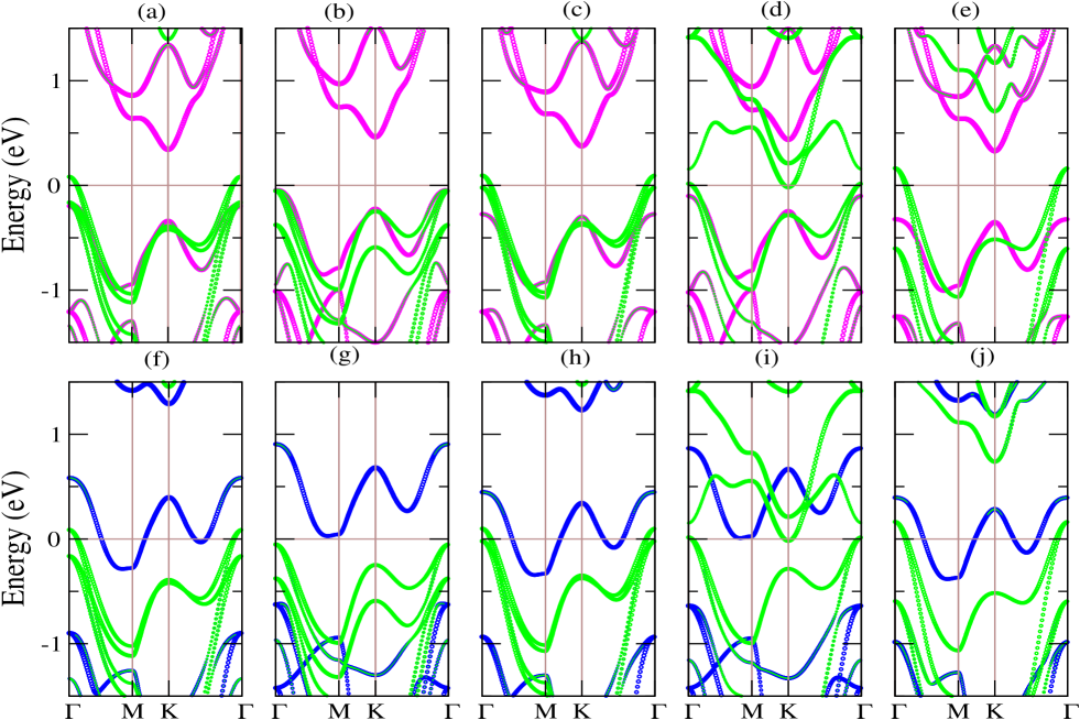
Figure 5 shows the spin-projected band structures of these trilayer arrangements of VSe2-Sc2CO2 heterostructure.Among the three arrangements with VSe2 as the intermediate layer, half-metallic ground state is observed for Sc2CO2(P)/VSe2/Sc2CO2(P) (Figure 5(a),(f)) and Sc2CO2(P)/VSe2/Sc2CO2(P)(Figure 5(c),(h)). In both cases, the spin-down(spin-up) band is metallic (semiconducting). In contrast, Sc2CO2(P)/ VSe2/ Sc2CO2(P) heterostructure is semi-conducting in both spin channels (Figure 5(b),(g)). Thus, semiconductor to half-metallic ground state can be realized in these tri-layer heterostructures by changing polarisations of the MXene layers through the application of an external electric field. This implies that the tri-layer heterostructures of Sc2CO2-VSe2 with the latter sandwiched between two MXene layers can act as a multiferroic. This is not so with the other two tri-layers, which basically are heterostructures of a bi-layer Sc2CO2 and a mono-layer of VSe2.Upon reversal of polarisation in the bi-layer Sc2CO2 from P to P, the heterostructure ground state changes from a semi-metallic to a metallic one only(Figures 5(d),(i) and 5(e),(j) ).
III.4 Coupling Mechanism and interfacial interaction in Sc2CO2/VSe2/Sc2CO2 heterostructure
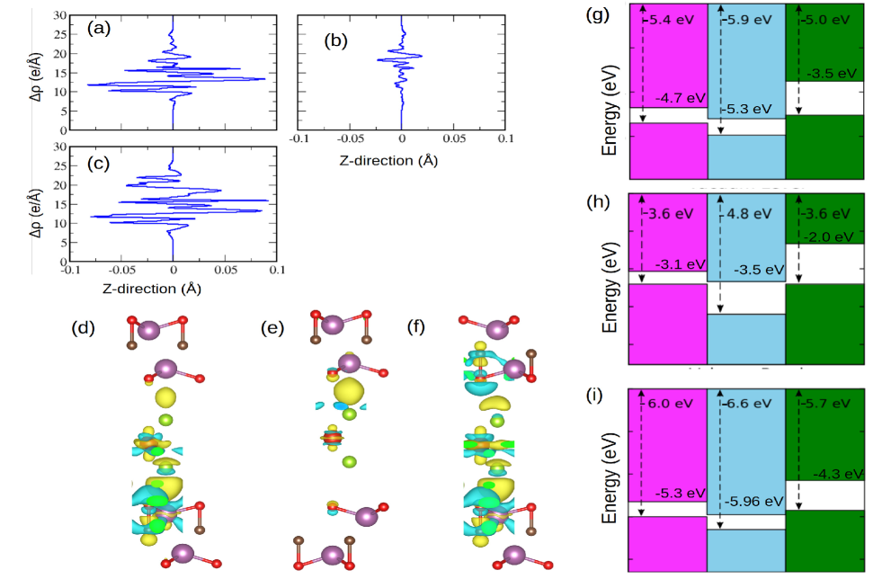
As observed in the case of the bilayer heterostructures, the changes in the electronic structures with stacking and/or electric polarization can be understood through an analysis of charge transfers across the interfaces. The stacking of layers in Sc2CO2(P)/VSe2/Sc2CO2(P) (Figure 4(a)) resembles a combination of two bi-layers VSe2-Sc2CO2(P) (Figure 1(g)) and VSe2-Sc2CO2(P) (Figure 1(h)). The top (bottom) surface of the tri-layer has the Cbottom(Ctop) side of MXene Sc2CO2 interfacing with VSe2. Since the differences in the Work functions of Ctop(Cbottom) side of Sc2CO2 and VSe2 is small(large), the charge transfer across the top (bottom)interface of the tri-layer heterostructure should be negligible (significant) as was the cases for the bi-layer heterostructures. The variations in the plane averaged differential charge density with (Figure 6(a)) and the charge density differences (Figure 6(d)) demonstrate this. Due to such charge transfer, the spin-down conduction band of VSe2 shifts downwards in the energy, closing the semiconducting gap and resulting in a metallic behavior in this spin channel. This makes the ground state of this tri-layer heterostructure half-metallic. The alignment of bands in this heterostructure, shown in Figure 6(g), indicates a broken gap type-III band alignment.
In contrast,in Sc2CO2(P)/VSe2/Sc2CO2(P) both interfaces consist of Cbottom part of Sc2CO2(Figure 4(b)). The expectation, therefore, is that apart from the small charge transfer due to the internal electric field, there will be no significant charge transfer across the interfaces. Consequently, the Sc2CO2(P)/VSe2/Sc2CO2(P) heterostructure will have a gap opening in both spin channels making the system semiconducting. This explains the band structure corresponding to this heterostructure (Figure 5(b)). The variations in the planar averaged differential charge density (Figure 6(b)) and the charge density differences (Figure 6(e)) support this argument. The band alignment diagram of this heterostructure, shown in Figure 6(h), indicates a band alignment of Type-I.
In the Sc2CO2(P)/VSe2/Sc2CO2(P) configuration shown in Figure 4(c), both interfaces consist of Ctop side of Sc2CO2.As a result, significant charge transfer occurs across both interfaces(Figures 6(c),(f)), leading to the closing of the semiconducting gap in the spin-down channel, making the ground state half-metallic. Consequently, the band alignment (Figure 6(i)) is a broken Type-III one. The results imply that by applying an electric field, one can switch between a type-I and a broken-gap Type-III system.
IV Applications
IV.1 Field-effect transistor(FET)
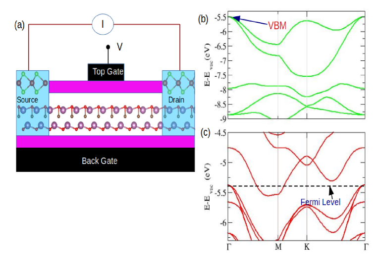
Since VSe2 becomes half-metallic when interfaced with Sc2CO2(P), it can form a van der Waals-contacted metal-semiconductor junction (MSJ) with Sc2CO2. Such MSJ can play a significant role in FET as the performance of the FET depends strongly on the height of the Schottky barrier(SB) across the junction[32] since this barrier provides resistance to charge carrier injection across the junction, the smaller the barrier, the lower the resistance, resulting in better FET performance. The SB height for hole injection can be estimated as . For electron injection, it is ; is the Fermi energy of the heterostructure while and are the conduction band minimum and the valence band maximum of semiconducting Sc2CO2. The schematic diagram for a field-effect transistor (FET) using this heterostructure is shown in Figure 7(a) while the position of the VBM of Sc2CO2 and Fermi level of the heterostructure is shown in Figure 7(b) and (c), respectively. The fermi level is slightly higher than VBM for the system under consideration. Consequently, is only 0.09 eV. This implies that the MSJ constructed out of this system will have a very small SB for hole injection. Further, for better performance of the FET, the semiconductor used in the heterostructure should also have a moderate bandgap and high carrier mobility. Sc2CO2, with a bandgap of 1.83 eV, is a moderate bandgap semiconductor. It is found to possess high hole mobility as well [21]. Thus, half-metallic VSe2-contacted Sc2CO2 FET will have a very small SB and a high on/off ratio.
IV.2 Prototype of a multiferroic memory
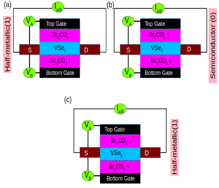
Two-dimensional (2D) ferroelectrics and 2D ferromagnets are promising nanodevices for information storage. While 2D ferromagnets suffer from non-volatility, 2D ferroelectrics are highly suitable for writing data but are less efficient for reading, the latter operation often being destructive. Memory devices constructed from Sc2CO2/VSe2 or Sc2CO2/VSe2/Sc2CO2 can overcome this difficulty. Non-volatile nanodevices for data storage can be constructed out of these heterostructures by utilizing the magnetoelectric coupling. In this nanodevice, the mechanism of data writing is the same as that of isolated monolayer Sc2CO2, achieved by switching the polarization state through the application of an electric field. Thus, isolated ferroelectrics’ efficient data writing properties are retained in these multiferroics. The data reading part is done the following way: the multiferroic heterostructure (both bilayer or trilayer structure) is a half-metal or semiconductor, depending on the polarization state of Sc2CO2. As a result, the electric signal of the heterostructure will differ from state to state. The destructive effect observed in monolayer ferroelectrics can be genuinely avoided by reading the magnetoelectric coupling-induced signal differences with a damage-free current [35]. A prototype of this device using trilayer Sc2CO2/VSe2/Sc2CO2 is shown in Figure 8. Here, the polarisation states of the two Sc2CO2 layers can be controlled by the application of two different voltages. Voltage VA, applied between the top gate and VSe2, helps to control the polarisation state of the top Sc2CO2 layer. Similarly, VB, applied between the bottom gate and VSe2, helps to control the polarisation state of the bottom Sc2CO2 layer.
V Conclusion
Using first-principles-based DFT calculations, we have demonstrated that the electronic properties of bi-layer VSe2/Sc2CO2 and tri-layer Sc2CO2/VSe2/Sc2CO2 heterostructures can be reversibly tuned through the application of an electric field. Depending on the polarization states of Sc2CO2, these heterostructures exhibit semiconducting or half-metallic behavior. The switching mechanism can be understood based on the charge redistribution across the heterostructure interface. The heterostructures exhibit broken-gap type-III band alignment in their half-metallic state, making them ideal for tunnel field-effect transistors (TFETs). Further, the magneto-electric coupling in these heterostructures leading to the electric-field controlled switching of the electronic state provides an ideal platform for a non-volatile atom-thick high-density data storage. Since a number of MXene Ferroelectrics with substantial polarization have been predicted from DFT-based high throughput calculations very recently [49], this work paves the ground for further exploration of MXene-TMDC heterostructures of different thicknesses towards the realization of more memory devices at the nanoscale.
References
- Yakout [2020] S. M. Yakout, Journal of Superconductivity and Novel Magnetism, 2020, 33, 2557.
- Sarma [2001] S. D. Sarma, American Scientist, 2001, 89, 516.
- Tian et al. [2012] Y. Tian, S. R. Bakaul and T. Wu, Nanoscale, 2012, 4, 1529.
- El-Ghazaly et al. [2020] A. El-Ghazaly, J. Gorchon, R. B. Wilson, A. Pattabi and J. Bokor, Journal of Magnetism and Magnetic Materials, 2020, 502, 166478.
- Lu et al. [2016] J. W. Lu, E. Chen, M. Kabir, M. R. Stan and S. A. Wolf, International Materials Review, 2016, 61, 456.
- Joshi [2016] V. K. Joshi, Engineering Science and technology, an International Journal, 2016, 19, 1503.
- Gurney [2008] B. A. Gurney, AAPPS Bulletin, 2008, 18, 18.
- Fert [2016] A. Fert, Angewandte Chemie International Edition, 2016, 19, 1503.
- Huang et al. [2017] B. Huang, G. Clark, E. Navarro-Moratalla, D. R. Klein, R. Cheng, K. L. Seyler, D. Zhong, E. Schmidgall, M. A. McGuire, D. H. Cobden et al., Nature, 2017, 546, 270.
- Gong et al. [2017] C. Gong, L. Li, Z. Li, H. Ji, A. Stern, Y. Xia, T. Cao, W. Bao, C. Wang, Y. Wang et al., Nature, 2017, 546, 265.
- Grönke et al. [2019] M. Grönke, B. Buschbeck, P. Schmidt, M. Valldor, S. Oswald, Q. Hao, A. Lubk, D. Wolf, U. Steiner, B. Büchner et al., Advanced materials interfaces, 2019, 6, 1901410.
- Wang et al. [2018] Z. Wang, T. Zhang, M. Ding, B. Dong, Y. Li, M. Chen, X. Li, J. Huang, H. Wang, X. Zhao et al., Nature nanotechnology, 2018, 13, 554.
- Sun et al. [2020] X. Sun, W. Li, X. Wang, Q. Sui, T. Zhang, Z. Wang, L. Liu, D. Li, S. Feng, S. Zhong et al., Nano Research, 2020, 13, 3358.
- Gong et al. [2019] Y. Gong, J. Guo, J. Li, K. Zhu, M. Liao, X. Liu, Q. Zhang, L. Gu, L. Tang, X. Feng et al., Chinese Physics Letters, 2019, 36, 076801.
- Huang et al. [2018] B. Huang, G. Clark, D. R. Klein, D. MacNeill, E. Navarro-Moratalla, K. L. Seyler, N. Wilson, M. A. McGuire, D. H. Cobden, D. Xiao, W. Yao, P. Jarillo-Herrero and X. Xu, Nature Nanotechnology, 2018, 13, 544.
- Jiang et al. [2018] S. Jiang, L. Li, Z. Wang, K. F. Mark and J. Shan, Nature Nanotechnology, 2018, 13, 549.
- Jiang et al. [2018] S. Jiang, J. Shan and K. F. Mark, Nature Materials, 2018, 17, 406.
- Wang et al. [2018] J. Wang, T. Zhang, M. Ding, B. Dong, Y. Li, M. Chen, X. Li, J. Huang, H. Wang, X. Zhao, Y. Li, D. Li, C. Jia, L. Sun, H. Guo, Y. Ye, D. Sun, Y. Chen, T. Yang, J. Zhang, S. Ono, Z. Han and Z. Zhang, Nature Nanotechnology, 2018, 13, 554.
- Deng et al. [2018] Y. Deng, Y. Yu, Y. Song, J. Zhang, N. Z. Wang, Z. Sun, Y. Yi, Y. Z. Wu, S. Wu, J. Zhu, J. Wang, X. H. Chen and Y. Zhang, Nature, 2018, 563, 94.
- Fei et al. [2018] Z. Fei, B. Huang, P. Malinowski, W. Wang, T. Song, J. Sanchez, W. Yao, D. Xiao, X. Zhu, A. F. May, W. Wu, D. H. Cobden, J. H. Chu and X. Xu, Nature Materials, 2018, 17, 778.
- Dong et al. [2019] S. Dong, H. Xiang and E. Dagotto, National Science Review, 2019, 6, 629.
- Gong et al. [2019] C. Gong, E. M. Kim, Y. Wang, G. Lee and X. Zhang, Nature Communications, 2019, 10, 2657.
- Sun et al. [2019] W. Sun, W. Wang, D. Chen, Z. Cheng and Y. Wang, Nanoscale, 2019, 11, 9931.
- Spaldin and Fiebig [2005] N. A. Spaldin and M. Fiebig, Science, 2005, 309, 391.
- Wan et al. [2019] S. Wan, Y. Li, W. Li, X. Mao, C. Wang, C. Chen, J. Dong, A. Nie, J. Xiang, Z. Liu et al., Advanced Functional Materials, 2019, 29, 1808606.
- Wang et al. [2020] L. Wang, X. Wang, Y. Zhang, R. Li, T. Ma, K. Leng, Z. Chen, I. Abdelwahab and K. P. Loh, Advanced Functional Materials, 2020, 30, 2004609.
- Yu et al. [2018] H. Yu, D. Gao, X. Wang, X. Du, X. Lin, W. Guo, R. Zou, C. Jin, K. Li and Y. Chen, NPG Asia Materials, 2018, 10, 882.
- Chang et al. [2016] K. Chang, J. Liu, H. Lin, N. Wang, K. Zhao, A. Zhang, F. Jin, Y. Zhong, X. Hu, W. Duan et al., Science, 2016, 353, 274.
- Liu et al. [2016] F. Liu, L. You, K. L. Seyler, X. Li, P. Yu, J. Lin, X. Wang, J. Zhou, H. Wang, H. He et al., Nature Communications, 2016, 7, 1.
- Noor-A-Alam and Nolan [2023] M. Noor-A-Alam and M. Nolan, ACS Applied Materials & Interfaces, 2023, 15, 42737.
- Kohn and Sham [1965] W. Kohn and L. J. Sham, Physical Review, 1965, 140, A1133.
- Zhao et al. [2019] Y. Zhao, J.-J. Zhang, S. Yuan and Z. Chen, Advanced Functional Materials, 2019, 29, 1901420.
- Liu et al. [2023] G. Liu, T. Chen, G. Zhou, Z. Xu and X. Xiao, ACS sensors, 2023, 8, 1440–1449.
- Wu et al. [2024] C. Wu, S. Sun, W. Gong, J. Li and X. Wang, Physical Chemistry Chemical Physics, 2024, 26, 5323.
- Cao et al. [2022] L. Cao, X. Deng, G. Zhou, S.-J. Liang, C. V. Nguyen, L. Ang and Y. S. Ang, Physical Review B, 2022, 105, 165302.
- Song et al. [2024] L. Song, R. Ye, C. Su, C. Wei, D. Chen, X. Liu, X. Zheng and H. Hao, Physical Review B, 2024, 109, 094105.
- Liu and Ke [2024] G. Liu and S. H. Ke, Physical Review Applied, 2024, 21, 044033.
- Chandrasekaran et al. [2017] A. Chandrasekaran, A. Mishra and A. K. Singh, Nano Letters, 2017, 17, 3290.
- You et al. [2022] J. You, J. Pan, S.-L. Shang, X. Xu, Z. Liu, J. Li, H. Liu, T. Kang, M. Xu, S. Li et al., Nano Letters, 2022, 22, 10167.
- Kresse and Furthmüller [1996] G. Kresse and J. Furthmüller, Physical Review B, 1996, 54, 11169.
- Kresse and Joubert [1999] G. Kresse and D. Joubert, Physical Review B, 1999, 59, 1758.
- Perdew et al. [1996] J. P. Perdew, K. Burke and M. Ernzerhof, Physical review letters, 1996, 77, 3865.
- Grimme et al. [2010] S. Grimme, J. Antony, S. Ehrlich and H. Krieg, The Journal of chemical physics, 2010, 132, 154104.
- Monkhorst and Pack [1976] H. J. Monkhorst and J. D. Pack, Phyical Review B, 1976, 13, 5188.
- Wang et al. [2021] X. Wang, D. Li, Z. Li, C. Wu, C.-M. Che, G. Chen and X. Cui, ACS Nano, 2021, 15, 16236.
- Fuh et al. [2016] H.-R. Fuh, C.-R. Chang, Y.-K. Wang, R. F. Evans, R. W. Chantrell and H.-T. Jeng, Scientific Reports, 2016, 6, 32625.
- Wang et al. [2023] Z. Wang, N. Qiu, E. Wu, Q. Huang, P. An, H. He and S. Du, Journal of Materials Research and Technology, 2023, 24, 173.
- Li et al. [2012] X. Li, X. Wu, Z. Li, J. Yang and J. Hou, Nanoscale, 2012, 4, 5680.
- Zhang et al. [2020] L. Zhang, C. Tang, C. Zhang and A. Du, Nanoscale, 2020, 12, 21291.