Calibration of cascaded phase shifters using pairwise scan method in silicon photonics integrated chip
Abstract
Cascaded phase shifters (CPSs) based on silicon photonics integrated chips play important roles in quantum information processing tasks. Owing to an increase in the scale of silicon photonics chips, the time required to calibrate various CPSs has increased. We propose a pairwise scan method for rapidly calibrating CPSs by introducing equivalent Mach Zehnder Interferometer structures and a reasonable constraint of the initial relative phase. The calibration can be nearly completed when the scanning process is finished, and only a little calculation is required. To achieve better performance, the key components, thermal optical phase shifter and 50/50 multimode interference coupler, were simulated and optimized to prevent thermal crosstalk and ensure a good balance. A 6-CPSs structure in a packaged silicon photonics chip under different temperature was used to verify the rapid pairwise scan method, and a fidelity of 99.97 was achieved.
Index Terms:
Integrated optics, Quantum information, Cascaded phase shifters, Mach Zehnder Interferometer, Fidelity.I Introduction
Silicon photonics integrated chips offer attractive advantages in quantum information processing tasks [1, 2, 3, 4, 5, 6, 7], such as large-scale integration [8, 9, 10], complementary metal-oxide semiconductor compatibility [11, 12], telecommunication wavelengths operation [13], integrated photon sources [14, 15, 16], programmable quantum circuits [17, 18, 19], quantum key distribution [20, 21, 22, 23], and integrated photon detectors [24, 25, 26]. To ensure correct operation of the quantum circuits, the calibration of the components in the quantum circuits is necessary. The calibration of numerous phase shifters has become increasingly complex owing to an increase in the scale of quantum photonics chips. A representative example is the cascaded phase shifters (CPSs) in a fully programmable two-qubit quantum processor [3, 27]. There are a total of eight 5-CPSs in the quantum processor. Each 5-CPSs can be used to prepare initial single-qubit states and implement single-qubit operation. The structure of CPSs comprises a series of 50/50 multimode interference (MMI) couplers and parallel waveguides with phase shifters between them. By varying the relative phase of the two parallel waveguides, the specified function can be accomplished. However, owing to fabrication errors, the initial relative phase is usually not zero, and the linear relationship between the heating power and shifted phase for each phase shifter is not identical. Thus, CPSs should be calibrated prior to use in a quantum information processing task.
The traditional method for calibrating the CPSs structure requires a lot of calculation, which increases exponentially with the series number of CPSs [3]. Later, a calibration method whose amount of calculation linearly increasing with the series number was proposed and demonstrated[28, 29]. In this paper, we propose a pairwise scan method for calibrating CPSs. The proposed method introduced an equivalent transform of Mach Zehnder Interferometer (MZI) structures that can simplify CPSs structures. Using this method, CPSs can be calibrated by scanning pairs of thermal optical phase shifters (TOPSs) stepwise. After scanning, the calibration is nearly completed, only a little calculation is required. To simplify the calibration, the pairwise scan method utilizes the constraint that the initial relative phase, , satisfies , which is a reasonable assumption for mature fabrication technology. A method for calibrating CPSs without the constraint is also proposed and demonstrated. To reasonably design the TOPS, we simulated the temperature distribution around TOPS on the silicon-on-insulator (SOI) platform, a safe distance is designed to prevent the thermal crosstalk between TOPSs. Furthermore, the 50/50 MMI structure was optimized to reduce calibration error. Finally, the average fidelity of 99.97 was achieved by using a 6-CPSs structure in a packaged silicon photonics chip.
II CPSs calibration methods
During the calibration of CPSs, we discriminate the methods as odd or even pairwise scan methods according to the series of phase shifters.
In the odd pairwise scan method, is expressed as
| (1) |
In the even pairwise scan method, is expressed as
| (2) |
The structure of 1-CPS is the simplest among the odd CPSs, and the structure of 2-CPSs is the simplest among the even CPSs. They are both fundamental structures. In the following part, we will discuss the calibrations of 1-CPS, 2-CPSs, even CPSs, and odd CPSs.
II-A Calibration of 1-CPS
Fig. 1(a). shows the structure of 1-CPS, which is a typical MZI structure that has been widely used in silicon photonics [30, 31, 32, 33, 34, 35, 36, 17]. The initial relative phase of the two parallel waveguides is , and the relative phase generated by TOPS is , which has a linear relationship with the heating power that applied. The total relative phase is expressed as
| (3) |
The Jones Matrix of 1-CPS is represented as
| (4) | ||||
where is the Jones Matrix of MMI, and is the Jones Matrix of phase shift in upper arm.
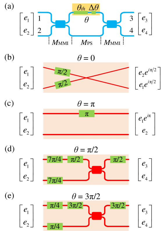
The laser beams guided into ports 1 and 2 are denoted as and , respectively. Their normalized intensities satisfy the following equation
| (5) |
The Jones vector of the input beams can be expressed as
| (6) |
Typically, only the relative phase is relevant, and the global phase can be neglected.
When , can be transformed into
| (7) |
In this case, the 1-CPS is equivalent to the cross-connection structure (Fig. 1 (b)).
When , can be transformed into
| (8) |
In this case, the 1-CPS is equivalent to the direct-connection structure (Fig. 1 (c)).
When , can be transformed into
| (9) |
In this case, the 1-CPS is equivalent to a MMI with two phase delays, , placed before and after it, respectively (Fig. 1 (d)).
When , can be transformed into
| (10) |
In this case, the 1-CPS is equivalent to a MMI with two phase delays, , placed before and after it (Fig. 1 (e)).
For any relative phase, , when the input beam is , the output beams are
| (11) |
Their corresponding intensities are
| (12) |
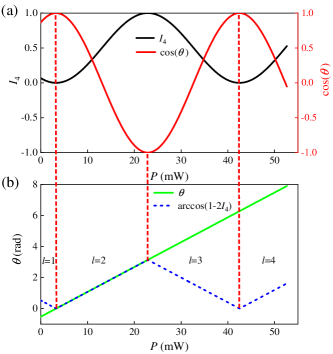
During the calibration of 1-CPS, we only use ports 2 and 4. The laser beam injects into port 2, and outputs from port 4. The relationship between the intensity, , and the applied heating power, , on the TOPS is represented by the black curve shown in Fig. 2 (a). Thus, the relationship between and can be derived using Eq. 12 (red curve, Fig. 2 (a)).
By calculating the inverse function of , blue dashed line were obtained (Fig. 2 (b)). The linear relationship (green line, Fig. 2 (b)) of relative phase and heating power is determined by correcting the blue dashed line using the following equation:
| (13) |
where the positive integer, , represents the blue dashed line segments. By fitting the corrected line, we obtain the following linear equation:
| (14) |
where is the slope, and is the intercept. The constraint, , is used to ensure the value of .
In the experiment, to ensure that the initial relative phase, , the lengths of both parallel waveguides should be short and equal during the design process. When the optical path of the upper waveguide is shorter, the initial relative phase , and the initial value of is 1. Thus, it is necessary to compensate for a phase shift, , to ensure that the optical path is equal or that the relative phase is . When the optical path of the upper waveguide is longer, the initial relative phase , and the initial value of is 2. It is necessary to compensate a phase shift to ensure that the optical path difference is half a wavelength or .
II-B Calibration of 2-CPSs
Fig. 3 (a) shows the structure of 2-CPSs. The relative phases of the two pairs of waveguides are and , respectively. Each relative phase has its initial relative and TOPS phases. They have a relationship similar to that in Eq. 3 as follows:
| (15) |
When the input beams are , the output beams are
| (16) | ||||
Their corresponding intensities are
| (17) |
The pairwise scan method is employed for the calibration of 2-CPSs. The flowchart is shown in Fig. 3 (b). When the laser beam transmits from ports 2 to 4, we scan the 2nd TOPS with step and a scanning scope . For each scanning step of the 2nd TOPS, we scan the 1st TOPS with step and a scanning scope . The peak-to-peak value output from the port 4 is denoted as .
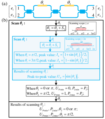
Based on Eq. 17 and the constraint , we can infer that the first minimum peak-to-peak value corresponds to the relative phase or . The heating power applied to 2nd is denoted as . The first maximun peak-to-peak value corresponds to the relative phase . The heating power applied to 2nd is denoted as .
When the heating power applied to the 2nd TOPS is , we have . Thus, Eq. 18 can be rewritten as
| (18) |
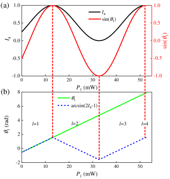
During the experiment, we determine the relationship between the intensity, , and applied heating power, (black curve, Fig. 4 (a)). Using Eq. 18, the relationship between and can be determined (red curve, Fig. 4 (a)). By calculating the inverse function of , we obtain the blue dashed line (Fig. 4 (b)). The green linear relationship between and was determined by correcting the blue dashed line using the following equation:
| (19) |
where the positive integer, , represents the blue dashed line segments. By fitting the green line, we obtain the following linear equation:
| (20) |
The is the slope, and the is the intercept. Note that the constraint should be used to ensure the value of .
By interchanging the scanning of 1st and 2nd TOPSs, a linear equation of the 2nd TOPS can be determined by the same way.
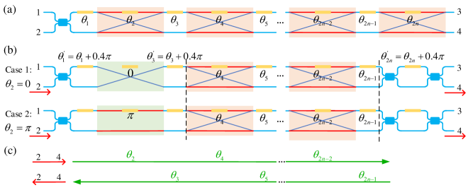
II-C Calibration method for even CPSs
Fig. 5 (a) shows the structure of even CPSs. The total number of TOPSs is , and the relative phase of the phase shifter is
| (21) |
where is the initial relative phase of the parallel waveguide, is the phase generated by TOPS, and is the heating power applied to the TOPS.
For the even CPSs, all the values of and should be calibrated. Using the pairwise scan method, we firstly calibrate the and from the right side of the structure by transmitting the laser beam from ports 2 to 4. For clarity, the Jones vectors of laser beams prior to and after the TOPS are denoted as and , respectively. Then, the Jones vector before the TOPS is denoted as , , here is the relative phase of the laser beams. Thus, the Jones vector of the laser beams output from ports 3 and 4 is
| (22) |
The intensity of the laser beam output from port 4 is
| (23) | ||||
When or , remains constant, independent of the values of and . This conclusion can also be achieved from the equivalent structure as shown in Fig. 5 (b). When or , the MZI structure with the TOPS is equivalent to the cross or direct-connection structure. In this case, the intensity, , was independent of the value of and .
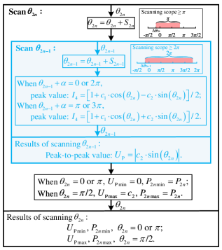
We first scan the 2th TOPS with step and a scanning scope as shown in Fig. 6. For each scanning step of the 2th TOPS, we performed a scan to the TOPS with step and a scanning scope . The peak-to-peak value of obtained by scanning the TOPS is denoted as . The first minimum peak-to-peak value is denoted as , and the heating power applied to the TOPS is denoted as . In this case, or , and . Combining the characters of Jones vectors and Eq. 23, we can get
| (24) |
The first maximum peak-to-peak value is denoted as , and the heating power applied to the TOPS is denoted as . In this case, . Eq. (23) is simplified to
| (25) |
By calculating the inverse cosine function similar to Eq. 13, we obtain the following linear equation:
| (26) |
Thus, the calibration of was completed. Owing to the relative phase of , could not be calibrated using Eq. 26. However, we obtain when or , or we can say that we calibrate the relative phase, . Next, this result is subsequently used to calibrate .
After the aforementioned steps, we apply to the TOPS. In this case, the MZI structure is equivalent to the cross or direct-connection structure. Thereafter, we pairwise-scan and calibrate the and TOPSs as the and TOPSs.
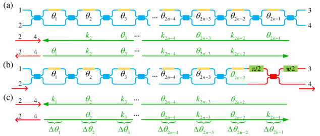
Using the pairwise scan methods above from right to left in a stepwise manner, we calibrate the relative phase, , of all the even-number TOPSs and the slope, , of all the odd-number TOPSs (Fig. 5 (c)).
Thereafter, we change the transmission of laser beams from right to left. Using the pairwise scan methods above stepwise from left to right, we calibrate the of all the odd-number TOPSs and the of all the even-number TOPSs (Fig. 5 (c)).
For any TOPS, the applied heating power, , corresponding to or is calibrated, and the thermal relative phase could be calculated. Combining constraint and Eq. 21, we calibrate the initial relative phase, . Finally, we calibrate all the TOPSs in the even CPSs.
In the even CPSs calibration, the constraint is used to simplify the calibration. Even if no constraint exists, the initial relative phase, , is calibrated from 2nd to ()th TOPSs. Details regarding the non-constraint even CPSs calibration method are provided in Appendix A.
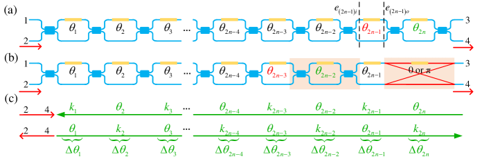
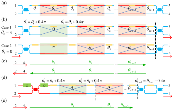
II-D Calibration odd CPSs
Fig. 7 shows the structure of odd CPSs, and the total number of TOPSs is . According to the calibration method of the even CPSs, we calibrate the relative phase, , of the odd-number TOPSs () and the slope, , of the even-number TOPSs (). However, from left to right, the calibrated items are also the () of the odd-number TOPSs and () of the even-number TOPSs (Fig. 7 (a)). Thus, to calibrate the of the even-number TOPSs and the of the odd-number TOPSs, we introduce an equivalent structure of the TOPS (Fig. 7 (b)). In this case, the heating power, , is applied to the TOPS to obtain . Thereafter, we calibrate the () of the even-number TOPSs and the () of the odd-number TOPSs from right to left when the laser beam transmits from ports 2 to 4 (Fig. 7 (c)). Using a similar method, when the laser beam transmits from ports 4 to 2, we can calibrate the () of the even-number TOPSs and the ( of the odd-number TOPSs. Combining the calibration results shown in Fig. 7 (a) and (c), we can calibrate all the and of odd CPSs.
The equivalent transform of the MZI structure introduces a phase shift. When we calibrate the CPSs from right to left, the relative phase, , should be 0 or . was in a similar situation.
Using the odd CPSs calibration method, constraint is used to simplify the calibration. Even if no constraint existed, the initial relative phase, , is calibrated from 2nd to ()th TOPSs. Details of the non-constraint odd CPSs calibration method are available in Appendix B.
III Optimization of key CPS components
The TOPS and 50/50 MMI are key components of the CPS. The thermal crosstalk and phase-power linearity of the TOPS, and the balance of the 50/50 MMI are closely related to the precision of calibration. To realize better calibration results, we simulate and optimize the structures of the key components.
III-A Simulation of TOPS
The principle of TOPS is based on the thermal optical effect of silicon, which implies that effective refractive index, , of silicon varies with temperature as follows:
| (27) |
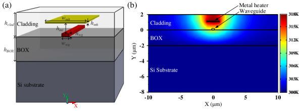
where is the thermal optical coefficient of silicon in the C band over the temperature range of 300–600 K [37]. The linear term plays a dominant role within this range. Fig. 8 (a) shows the TOPS structure on the SOI platform. It comprises a silicon waveguide (red) and metal heater (yellow) above it. The metal heater transforms the electric energy into thermal energy,
| (28) |
where is the heating power of TOPS, is the voltage applied to the metal heater, and is the resistance of the metal heater. The heating power changes the temperature of waveguide and the effective refractive index, . During the simulation, the heating power is set to set to 20 mW. The thicknesses of the buried oxide (BOX) layer, , and cladding layer, , are both 2 m, and the thickness of the Si substrate is 750 m. The silicon waveguide is on the bottom of the cladding layer (width, m; height, m). The metal heater is approximately in the middle of the cladding layer (width, m; height, m). The interval between the metal heater and the waveguide is m. The materials of BOX and cladding layer are \ceSiO2, and that of the metal heater is Titanium nitride (TiN).
The temperature distribution of the SOI chip is simulated using the Heat Transport (HEAT) solver of Ansys Lumerical by solving the following heat conduction equation:
| (29) |
where is the mass density (), is the specific heat (), is the heat conductivity (), and is the heat energy transfer rate () [38]. is calculated by
| (30) |
where m is the length of the metal heater. The length satisfies and ; thus, the structure was assumed to exhibit translational symmetry, and Fig. 8 (b) shows the cross-section of the temperature distribution.
The top of the device was bounded by air. During the simulation, the heat convection boundary condition, , was applied to the top surface of the cladding, where was the direction normal to the surface and was the convection heat coefficient of the surrounding air. The Dirichlet boundary condition was applied to the bottom surface of the Si substrate. The temperatures of the top and bottom boundaries were set to K. The left and right boundaries of the simulation region were 25 m away from the TOPS structure such that there was practically no temperature variance at these boundaries. It is reasonable to set the boundary condition as thermal isolation. Table I lists the parameters of various materials used in the simulation.
| Material | |||
| () | () | () | |
| Si | 2330 | 711 | 148 |
| \ceSiO2 | 2203 | 709 | 1.38 |
| TiN | 5430 | 604.45 | 67.7 |
| air | 1.17 | 1006.43 | 0.026 |
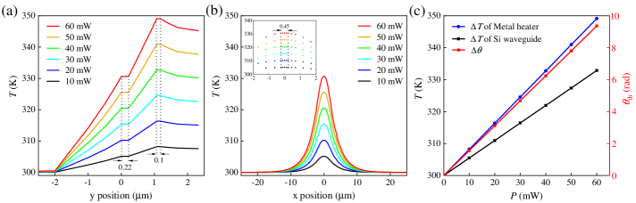
When we changed the heating power of the heater, the temperature distribution curves in direction at m are shown in Fig. 9 (a). Considering that the heater conductivity, , of silicon and the metal heater considerably exceeded that of the surrounding \ceSiO2, the temperature in the waveguide and metal heater was uniform. Similarly, the temperature of the Si substrate was also uniform and close to the . The temperature distribution curves in the direction at m with different heating power are shown in Fig. 9 (b). The peak value of each curve represents the temperature of the silicon waveguide. A good linear relationship exists between the temperature (black line, Fig. 9 (c)) and the heating power applied to the TOPS. Similarly, the linear blue line represents the temperature of the metal heater versus the heating power.
The maximum applied voltage in the experiment was 10 V, and the resistance of the metal heater was approximately 1.75 k. Thus, the maximum heating power applied to the TOPS was 57 mW. The maximum heating power of 60 mW was adopted during the simulation. The simulation results showed that when the center distance of the TOPSs exceeded 40 m, nearly no thermal crosstalk was observed under the condition that the temperature was controlled. In addition, we have also performed a similar simulation along the direction of waveguide. Even if the heat conduction of Si is high, the simulation show that the temperature is close to the boundary temperature (300 K) when the length of waveguide not below the heater is above 20 m. Thus thermal crosstalk between CPSs is negligible considering the distance of 23 m between the heater and the MMI and waveguide length is 71 m.
We used the finite element eigenmode solver to calculate the phase shift for different heating powers. The phase shift, , of a TOPS is dependent on the change in the effective refractive index, , and length, m, of the waveguide. It can be expressed as
| (31) |
where m represents the wavelength of the laser, and can be calculated using Eq. 27 [39]. Based on the simulation results (black line, Fig. 9 (c)), the relationship between the phase shift and heating power is shown as the red line with a slope of rad/mW. It slightly exceeded the experimental result ( rad/mW). The main reason is that the metal (Al) used to connect the metal heater (TiN) absorbed part of heat quantity in a realistic situation.
The simulation revealed the temperature distribution of the TOPS on SOI platform. Importantly, a good linear relationship was observed between the phase shift of the TOPS and the applied power. The consumed heating power of the phase shift, , was approximately 20.2 mW. Note that, we can infer the safe distance to prevent the thermal crosstalk of TOPSs.
III-B Simulation of 50/50 MMI
The balance degree of the 50/50 MMI is a key parameter that directly affects the accuracy of the calibration results of CPS [29]. Fig. 10 (a) shows an optimized structure of the 50/50 MMI using the eigenmode expansion (EME) solver of Ansys Lumerical. The structure was fabricated based on a 70 nm-etched slab waveguide. Its core length and width were m and m, respectively. The two input ports were ports 1 and 2, and the two output ports were ports 3 and 4. The imbalance degree, of two output intensities is usually defined as
| (32) |
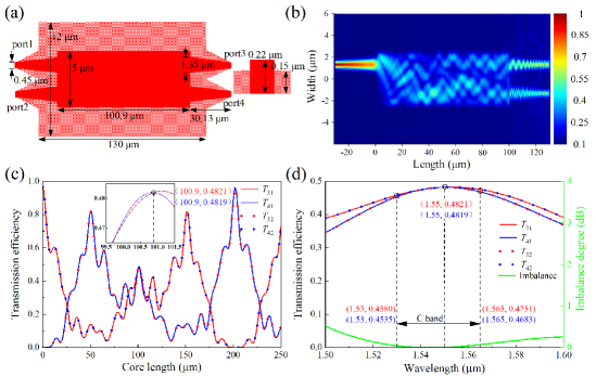
where and are the transmission efficiencies from port 1 to ports 3 and 4, and and are the transmission efficiencies from port 2 to ports 3 and 4 [40]. Fig. 10 (b) shows the top view of the simulated optical power distribution at 1550 nm. The source span was set to 2 m 2 m during the simulation, and the laser beams were in the transverse electric (TE) mode in the structure.
Fig. 10 (c) shows the transmission efficiency versus the core length when the wavelength of laser beam was 1550 nm. and were represented by the red and blue curves, respectively. and were represented by the red and blue dotted line, respectively. The sweep range of the core length, , was 0–250 m with an interval of 1 m. The laser beams input from ports 1 and 2 exhibited good symmetrical characteristics. The splitting ratio varied with the . We find that the 50/50 ratio corresponds to the core length of approximately 101 m. To simulate the balance degree with high precision, a small scan interval of 0.1 m was employed (inset in Fig. 10 (c)). The core length 100.9 m corresponds to a imbalance degree of approximately 0.0018 dB with and . An extinction ratio of 73.5 dB can be achieved if the MMI was used to construct the 1-CPS or MZI. Fig. 10 (d) shows the transmission efficiency and imbalance as a function of wavelength at the core length of 100.9 m. The red and blue curves represent and , respectively. The red and blue dotted curves represent and , respectively. The green curve shows that the imbalance degree varied with the wavelength. The simulated imbalance was lower than 0.063 dB in the range of C wave band (1530–1565 nm), and the extinction is higher than 42.8 dB.
In the experiment, the extinction ratio of several 1-CPSs were tested and were observed to exceed 50 dB, which was lower than the optimized value (73.5 dB) owing to the imperfections in fabrication. The 50 dB extinction ratio corresponds to an imbalance degree about 0.027 dB. With this imbalance degree, a calibration fidelity of 99.991 can be achieved. The reason can be seen in Appendix C. Thus, the realistic imbalance was sufficiently low to achieve a high fidelity. The method for calculating the fidelity is described in Section IV-C.
IV Experimental calibration of 6-CPSs
To verify the feasibility of the pairwise scan calibration method, a 6-CPSs was designed and fabricated using the industry-standard SOI technology of CUMEC [42]. The experimental setup and calibration results are as follows.
IV-A Experimental setup
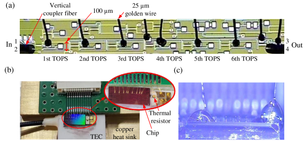
Fig. 11 (a) shows the microphotograph of 6-CPSs in the silicon photonics chip. The distance of the upper and lower waveguides between the MMIs is 100 m. The upper and lower waveguides both had TOPS for symmetry and backup. The upper TOPSs were used in the experiment. Ports 2 and 4 were one-dimensional (1D) grating couplers and were used to vertically couple the waveguides and single-mode fibers whose diameter was 125 m. Fig. 11 (b) shows the packaged chip. The heaters of the TOPSs were wire bonded to printed circuit board pads using 25 m golden wire. The entire silicon photonics chip adhered to the surface of the thermoelectric cooler (TEC) using thermal conductive adhesive. The thermal resistor was welded on a mount with good thermal conductivity. The mount was fixed on the TEC surface with thermal conductive adhesive and placed next to the chip to monitor its temperature. The TEC was mounted onto a copper heat sink. To enhance the calibration stability, ultraviolet (UV) glue was used in vertical coupling packaging (Fig. 11 (c)). The packaging increased the vertical coupling loss from 4.5 to 5.5 dB, and the total insertion loss of the chip was 12 dB.
IV-B Calibration results
During the experiment, two synchronized multifunction I/O cards (NI, USB6259) with six 16-bit digital-to-analog converters (DACs) were used to apply the voltage signals to the six TOPSs. A high resolution of 0.3 mV, which corresponds to a phase resolution of less than 0.028∘or radians, can be achieved when the output range is 10 V [41]. During the experimental scanning process, the scanning range was 0–10 V, and the scanning step was 0.01 V corresponding to a phase resolution below 0.97∘or radians. The wavelength of the laser was 1550 nm, and the input optical power was 1 mW. The output laser was detected using a photodetector, and the output electrical signal was collected using an analog-to-digital converter (ADC; USB6259).
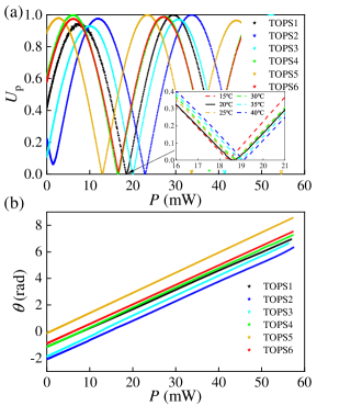
During the CPSs calibration process, the temperature of the TEC was set to 20 ∘C. When the laser beam transmitted from ports 2 to 4, we firstly calibrated the relative phase, , of the 6th TOPS and the slope, , of the 5th TOPS. For each scan step of the 6th TOPS, the peak-to-peak value obtained by scanning the 5th TOPS was recorded as . When the first pairwise scan was completed, the trace of the peak-to-peak value, , was plotted (red curve, Fig. 12 (a)). The first appearance of the maximum, , corresponded to , and its applied heating power was . The first appearance of the minimum, , corresponded to with a value of 0 or , and the applied heating power was . In this case, the normalized intensity of the laser beam output from port 4 was a fixed value, . When the heating power of the 6th TOPS was , the orange line comprising asterisk points shown in Fig. 12 (b) was obtained by transforming the scan data of the 5th TOPS using the inverse cosine function. Through the linear fitting of the orange points, the slope, , was obtained. To calibrate the 4th and 3rd TOPS, was applied to the 6th TOPS such that it was equivalent to a cross or direct-connection structure.
Fig. 12 (a) shows the trace of the peak-to-peak value, , during calibration as a green curve, and Fig. 12 (b) shows the cyan line of 3rd TOPS. Using a similar procedure, we obtained blue, black, cyan, and orange curves (Fig. 12 (a)) corresponding to the peak-to-peak values of , , , and , respectively. The black, blue, green, and red asterisks in Fig. 12 (b) represent the data of the 1st, 2nd, 4th and 6th TOPS, respectively. Afterward, the slopes (, , and ) were obtained. Combining the , , and constraint , the initial phase, , is calculated by Eq. 14. Table II lists the calibration results for the 6-CPSs. The calibration results with constraint were consistent with the calibration results without constraint (Table A1).
| Result | 1st | 2nd | 3rd | 4th | 5th | 6th |
| TOPS | TOPS | TOPS | TOPS | TOPS | TOPS | |
| (mW) | 18.6075 | 1.4921 | 20.0369 | 16.5703 | 12.9558 | 16.4435 |
| (rad/mW) | 0.1427 | 0.1459 | 0.1515 | 0.1478 | 0.1517 | 0.1470 |
| (rad) | 0.4863 | -0.2177 | 0.106 | 0.6925 | 1.1762 | 0.7244 |
| (degree) | 27.86 | -12.47 | 6.07 | 39.68 | 67.39 | 41.5 |
| Result | 1th | 2th | 3th | 4th | 5th | 6th | mean | deviation | |
|---|---|---|---|---|---|---|---|---|---|
| 0.1428 | 0.1428 | 0.1427 | 0.1427 | 0.1427 | 0.1427 | 0.1427 | |||
| 15 ∘C | (rad) | 0.5039 | 0.5130 | 0.5043 | 0.5041 | 0.5047 | 0.5138 | 0.5073 | 0.0043 |
| (degree) | 28.87 | 29.39 | 28.90 | 28.88 | 28.92 | 29.44 | 29.07 | 0.2471 | |
| 0.1427 | 0.1427 | 0.1427 | 0.1427 | 0.1427 | 0.1427 | 0.1427 | |||
| 20 ∘C | (rad) | 0.4865 | 0.4954 | 0.4770 | 0.4863 | 0.4861 | 0.4770 | 0.4847 | 0.0063 |
| (degree) | 27.86 | 28.38 | 27.33 | 27.86 | 27.85 | 27.33 | 27.86 | 0.3628 | |
| 0.1432 | 0.1430 | 0.1428 | 0.1427 | 0.1431 | 0.1428 | 0.1429 | |||
| 25 ∘C | (rad) | 0.4583 | 0.4714 | 0.4658 | 0.4671 | 0.4695 | 0.4667 | 0.4665 | 0.0041 |
| (degree) | 26.26 | 27.01 | 26.69 | 26.76 | 26.90 | 26.74 | 26.73 | 0.2354 | |
| 0.1428 | 0.1428 | 0.1427 | 0.1431 | 0.1429 | 0.1434 | 0.1429 | |||
| 30 ∘C | (rad) | 0.4564 | 0.4574 | 0.4578 | 0.4414 | 0.4452 | 0.4452 | 0.4506 | 0.0068 |
| (degree) | 26.15 | 26.21 | 26.23 | 25.29 | 25.51 | 25.51 | 26.15 | 0.3876 | |
| 0.1427 | 0.1429 | 0.1432 | 0.1428 | 0.1429 | 0.1428 | 0.1429 | |||
| 35 ∘C | (rad) | 0.4490 | 0.4358 | 0.4301 | 0.4377 | 0.4358 | 0.4377 | 0.4377 | 0.0056 |
| (degree) | 25.72 | 24.97 | 24.64 | 25.08 | 24.97 | 25.08 | 25.08 | 0.3237 | |
| 0.1435 | 0.1428 | 0.1428 | 0.1428 | 0.1432 | 0.1429 | 0.1430 | |||
| 40 ∘C | (rad) | 0.4150 | 0.4189 | 0.4189 | 0.4283 | 0.4113 | 0.4075 | 0.4166 | 0.0066 |
| (degree) | 23.78 | 24.00 | 24.00 | 24.54 | 23.56 | 23.35 | 23.87 | 0.3775 |
Using the minimum slope and the maximun slop , a phase shift difference of 0.36 rad will be generated by applying 40 mW heating power that can cause a phase shift about . It means that of fixed slope value is used for all TOPSs, an error with almost the same magnitude to the initial relative phase can be generated. Therefore the accurate calibration of each TOPS is necessary.
Temperature is the major factor affecting the standrad deviation of the initial phase . To observe the influence of temperature, we set the temperature of the chip to 15 ∘C, 20 ∘C, 25 ∘C, 30 ∘C, 35 ∘C and 40 ∘C using TEC and calibrate the 1st TOPS at corresponding temperature. At each temperature, the 1st TOPS was calibrated six times. Table III presents the calibration results of the 1st TOPS.
The calibration results at the same temperature exhibited good consistency. The slope, , remained unchanged, and the maximum standard deviation was . The maximum standard deviation of the initial phase, , was 0.39∘. Comparing the results of different temperatures, we observed that between both arms gradually decreased with an increase in temperature. However, the slope remained unchanged. When the temperature was increased from 15 ∘C to 40 ∘C, the initial relative phase, , decreased by 5.2∘. The inset in Fig. 12 (a) shows during the calibration. In addition, the influence of temperature on the can also be inferred. gradually increased with an increase in temperature.
IV-C Fidelity testing
The fidelity was used to verify the accuracy of our CPSs calibration method. The TEC temperature was set to 20 ∘C, and a six-channel DAC was used to sequentially apply the scanning signals to the six TOPSs. The scanning range was 0–10 V with a scanning step of 0.01 V, which results in a 1000 scanning points for each TOPS. The expermental normalized intensity of the laser beam outputs from port 4 was defined as . To calculate the fidelity, the expected output intensity of the laser from port 4 is derived based on the theoretical 6-CPSs model constructed using the calibration results. Thereafter, 6000 fidelity values were calculated using the following equation [43]:
| (33) |
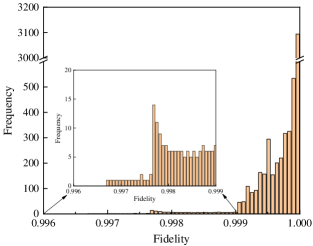
Fig. 13 shows the statistical results of the fidelity. The average, maximum, and minimum values were 99.97, 100, and 99.68, respectively. In addition, 96.6 of the data had a fidelity above 99.9.
V Conclusion
This paper reported a pairwise scan method that can rapidly calibrate the CPSs structure in a silicon photonics integrated chip. Four kinds of equivalent structure of 1-CPS and reasonable constraint were used to simplify the calibration. The calibration methods slightly differed according to the parity of the series number of CPSs. Using the pairwise scan method, only one input port and one output port are needed. This flexibility will make the calibration convenient when the CPSs are used to constitute more complex networks [3]. In addition, calibration methods without constraint were introduced. After the scanning process, only a little amount of calculation is required to accomplish the calibration.
To reasonably design the CPSs structure, the key components, the TOPS and 50/50 MMI, were simulated and optimized to prevent thermal crosstalk and obtain a better 50/50 splitting ratio. With the optimized 50/50 MMI, the extinction ratio of 1-CPS can exceed 50 dB, which can ensure that the theoretical fidelity exceeds 99.991. A 6-CPSs structure in a packaged silicon photonics chip under different ambient temperatures was used to verify the rapid pairwise scan method. The calibration results with the constraint coincides with the case without the constraint, and a fidelity of 99.97 was achieved. Our results can find practical applications on large-scale quantum circuits in photonics integrated chip. In our future work, we will try to improve the pairwise scan method to calibrate the Resh and Clements structures efficiently [44, 45, 46, 47, 48, 49].
Appendix A Method of calibrating in even CPSs without constraint
In the even CPSs, the calibration method introduced below did not require a constraint when calibrating from 2nd to th TOPSs.
The relative phase, , of each TOPS can be calibrated to either 0 or using the following even CPSs calibration method without constraint . When all the relative phases were set to 0 or , the MZI structures with the even-number TOPS are equivalent to the cross or direct-connection structures (Fig. A1 (a)). This was the initial state of the subsequent calibration, and the even CPSs were nearly equivalent to a MMI. When the input beam was , the output beam from the first MMI becomes . Subsequently, when the beams pass through the cross or direct-connection structure, the intensity remained at 1/2 even if the relative phases of the TOPSs were unknown.
To determine whether the relative phase was 0 or , 0.4 phase shifts were applied to the 1st and 3rd TOPS, which changed the relative phase to and , respectively. When , the MZI structure with the 2nd TOPS was equivalent to the cross structure (Fig. A1 (b)). The two 0.4 phase shifts applied to the 1st and 3rd TOPS act on different paths, which led to no relative phase change. When , the MZI structure with 2nd TOPS was equivalent to the direct connection structure. The two 0.4 phase shifts applied to the 1st and 3rd TOPS act on the same path, results in a 0.8 variation of the relative phase. To determine the changes in intensities due to 0 or 0.8, a 0.4 phase-shift voltage was applied to 2th TOPS, which changed the relative phase to . Considering that the Jones vector after the (2-1)th TOPS was , the intensity of the laser beam output from port 4 was
| (A1) |
where is the relative phase of the laser beams, and .
When , , we have
| (A2) |
When , , we have
| (A3) |
where denotes the total number of phase shifters with a phase shift of from the 1st to th TOPS. According to the value of , we can determine the exact value of .
Using the aforementioned method, we calibrated the relative phase of the even-number TOPSs (2, 4, …, , ) from left to right when the laser beams transmitted from ports 2 to 4 (Fig. A1 (c)). Similarly, the relative phase of the odd-number TOPSs (, , …, 5, 3) can be calibrated from right to left when the laser beams transmitted from ports 4 to 2.
| Result | 2nd | 3rd | 4th | 5th |
| TOPS | TOPS | TOPS | TOPS | |
| (rad) | 0 | |||
| (rad) | 0.2177 | 3.0356 | 2.4491 | 1.9654 |
| (rad) | -0.2177 | 0.106 | 0.6925 | 1.1762 |
Appendix B Method of calibrating in odd CPSs without constraint
In the odd CPSs, the calibration method introduced below did not require a constraint when calibrating from the 2nd to th TOPSs.
The relative phase, , of each TOPS can be calibrated to either 0 or using the odd CPSs calibration method without constraint. When all the relative phases are set to 0 or , the MZI structures with the even TOPS were equivalent to the cross or direct-connection structures. The odd CPSs were equivalent to an MZI structure (Fig. B1 (a)). This was the initial state of our the following calibration.
Similar to the method of calibrating the of even CPSs without constraint, we sequentially calibrate the of any even-number TOPSs (2, 4, …, , ) by applying 0.4 phase shifts to the two adjacent odd TOPSs. As shown in Fig. B1 (b), to determine whether the relative phase, , was 0 or , we applied 0.4 phase shifts to the 1st and 3rd TOPS, respectively. The Jones vector of the input beam from port 2 was . The Jones vector after the th TOPS was
| (B1) |
The intensities of the laser beam output from ports 3 and 4 were
| (B2) |
When , , we have
| (B3) |
When , , we have
| (B4) |
Here denotes the total number of phase shifters with a phase shift of from the 1st to th TOPSs. According to the value of , we calibrated the exact value of . Using the aforementioned method, we calibrated the relative phase of the even-number TOPSs (2, 4, …, , ) from left to right when the laser beams transmitted from ports 2 to 4 (Fig. B1 (c)). Considering that the number of CPSs was odd, when the direction of light transmitted changed, we only calibrated of the even TOPSs. The odd-number TOPSs (3, 5, …, ) could not be calibrated in this manner.
To calibrate the odd-number TOPSs, we added a phase shift to the 1th TOPS. Thus, the first MZI structure was transformed into a MMI with two phase delays, ( or ), placed before and after it, respectively (Fig. B1 (d)). After the transformation, the structure was similar to the even CPSs (Fig. A1 (b)) except for an additional phase shifter, , before the 2nd TOPS. When the input beam was at port 2, after the equivalent MMI and , the output beam became . In this case, to calibrate the 3th TOPS, we applied 0.4 phase shifts to the 2nd, 4th and th TOPS. The Jones vector after the th TOPS was denoted as
| (B5) |
The intensity of the laser beam output from port 4 was
| (B6) |
When , , we have
| (B7) |
When , , we have
| (B8) |
Here represents the total number of phase shifters with a value of from the 2nd to th TOPS. Subsequently, the odd-number TOPSs (3, 5, …, ) were calibrated (Fig. B1 (e)). Finally, we achieve the calibration of from the 2nd to th TOPSs in odd CPSs without constraint.
Appendix C The fidelity considering the biased splitting ratios ans unbalanced losses
To evaluate the effect of biased splitting ratios and unbalanced losses, we construct a MMI with a splitting ratio , and attenuation constants and , respectively. In this case, the matrix of MMI can be expressed as
| (C1) | ||||
When the Jones vector of the input beam is , the Jones vector of the output beam is
| (C2) |
The intensities of laser beams output from ports 3 and 4 are
| (C3) |
The imbalance degree, , of the MMI can be defined as
| (C4) |
where . For MZI or 1-CPS structure constructed by above MMI, when the Jones vector of input beam is , the Jones vector of output beam is
| (C5) | ||||
Their corresponding intensities are
| (C6) |
| (C7) |
The extinction ratio of the ports 3 and 4 can be expressed as
| (C8) | ||||
| (C9) |
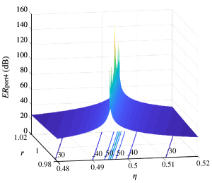
From the expression of , we can see that it has no relationship with . When the ratio approaches to 1, the approached to higher and infinite. The dependence of on and is shown in Fig. C1, the contours of different extinction ratios are plotted. For a constant value of , and has two nearly linear relationships.
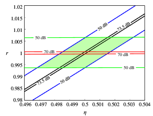
From the simulation results, we can obtain the transmission efficiencies and . In this case, the extinction ratio , the relationship of and is represented by the black solid lines in Fig. C2. The relationship of and at the is represented by blue lines. The is only related to . The values of at , are represented by the green lines and red lines, respectively. Obviously, we can use the extinction ratio to restrict the range of and . For example, will constraint and in the green area. In this case, the minimum fidelity is 99.991. When the extinction ratio increases, the ratio , the splitting ratio and the fidelity approaches to the ideal value of 1, 0.5, and 1, respectively.
From the above analysis, we can see that a measured extinction ratio greater than 50 dB can ensure the high fidelity greater than 99.991. The mature fabrication technology can make sure the consistency of the MZI structures in the 6-CPSs. Therefore, a fidelity greater than 99.97 is achieved in our experiment.
References
- [1] E. Pelucchi et al., “The potential and global outlook of integrated photonics for quantum technologies,” Nat. Rev. Phys., vol. 4, no. 3, pp. 194–208, Dec. 2021.
- [2] J. Wang, F. Sciarrino, A. Laing, and M. G. Thompson, “Integrated photonic quantum technologies,” Nat. Photonics, vol. 14, no. 5, pp. 273–284, May 2020.
- [3] X. Qiang et al., “Large-scale silicon quantum photonics implementing arbitrary two-qubit processing,” Nat. Photonics, vol. 12, no. 9, pp. 534–539, Sep. 2018.
- [4] S. Clemmen, K. P. Huy, W. Bogaerts, R. G. Baets, P. Emplit and S. Massar, “Continuous wave photon pair generation in silicon-on-insulator waveguides and ring resonators,” Opt. Express, vol. 17, no. 19, pp. 16558–16570, Sep. 2009.
- [5] D. Bonneau et al., “Quantum interference and manipulation of entanglement in silicon wire waveguide quantum circuits,” New J. Phys., vol. 14, no. 4, pp. 045003, Apr. 2012.
- [6] J. W. Silverstone et al., “On-chip quantum interference between silicon photon-pair sources,” Nat. Photonics, vol. 8, no. 2, pp. 104–108, Dec. 2013.
- [7] J. C. Adcock et al., “Advances in silicon quantum photonics,” IEEE J. Sel. Top. Quantum Electron, vol. 27, no. 2, pp. 1–24, Mar./Apr. 2021.
- [8] J. Wang et al., “Multidimensional quantum entanglement with large-scale integrated optics,” Science, vol. 360, no. 6386, pp. 285–291, Apr. 2018.
- [9] H. Wang et al., “Toward scalable boson sampling with photon loss,” Phys. Rev. Lett., vol. 120, pp. 230502, Jun. 2018.
- [10] J. Bao et al., “Very-large-scale integrated quantum graph photonics,” Nat. Photonics, vol. 17, no. 7, pp. 573–581, Apr. 2023.
- [11] S. Y. Siew et al., “Review of silicon photonics technology and platform development,” J. Lightwave Technol., vol. 39, no. 13, pp. 4374–4389, Jul. 2021.
- [12] S. Shekhar et al., “Roadmapping the next generation of silicon photonics,” Nat. Commun., vol. 15, no. 1, pp. 751, Jan. 2024.
- [13] D. Llewellyn et al., “Chip-to-chip quantum teleportation and multi-photon entanglement in silicon,” Nat. Phys., vol. 16, no. 2, pp. 148–153, Dec. 2019.
- [14] H. Takesue et al., “Generation of polarization entangled photon pairs using silicon wire waveguide.” Opt. Express, vol. 16, no. 8, pp. 5721–5727, Apr. 2008.
- [15] J. Wang et al., “Chip-to-chip quantum photonic interconnect by path-polarization interconversion,” Optica, vol. 3, no. 4, pp. 407–413, Apr. 2016.
- [16] M. Zhang et al., “Generation of multiphoton quantum states on silicon,” Light Sci. Appl., vol. 8, no. 1, p. 41, May 2019.
- [17] C. M. Wilkes et al., “60 dB high-extinction auto-configured Mach-Zehnder interferometer.” Opt. Lett., vol. 41, no. 22, pp. 5318–5321, Nov. 2016.
- [18] J. Carolan et al., “Universal linear optics,” Science, vol. 349, no. 6249, pp. 711–716, Jul. 2015.
- [19] N. C. Harris et al., “Quantum transport simulations in a programmable nanophotonic processor,” Nat. Photonics, vol. 11, no. 7, pp. 447–452, Jun. 2017.
- [20] Y. Bian et al., “Continuous-variable quantum key distribution over 28.6 km fiber with an integrated silicon photonic receiver chip,” Appl. Phys. Lett., vol. 124, pp. 174001, Apr. 2024.
- [21] P. Ye et al., “Transmittance-invariant phase modulator for chip-based quantum key distribution,” Opt. Express, vol. 30, no. 22, pp. 39911–39921, Oct. 2022.
- [22] G. Zhang et al., “Polarization-insensitive interferometer based on a hybrid integrated planar light-wave circuit,” Photonics Res., vol. 9, no. 11, pp. 2176–2181, Nov. 2021.
- [23] F. Wang, W. Wang, R. Niu, et al., “Quantum key distribution with on-chip dissipative kerr soliton,” Laser Photonics Rev., vol. 14, no. 2, pp. 1900190, Jan. 2020.
- [24] W. H. P. Pernice et al., “High-speed and high-efficiency travelling wave single-photon detectors embedded in nanophotonic circuits,” Nat. Commun., vol. 3, no. 1, pp. 1325, Dec. 2012.
- [25] F. Najafi et al., “On-chip detection of non-classical light by scalable integration of single-photon detectors,” Nat. Commun., vol. 6, no. 1, pp. 5873, Jan. 2015.
- [26] Y. Jia et al., “Silicon photonics-integrated time-domain balanced homodyne detector for quantum tomography and quantum key distribution,” New J. Phys., vol. 25, no. 10, pp. 103030, Oct. 2023.
- [27] A. M. Childs, “Secure assisted quantum computation,” Quantum Info. Comput., vol. 5, no. 6, pp. 456–466, Sep. 2005.
- [28] Z. Xing, Z. Li, T. Feng, and X. Zhou, “High-speed calibration method for cascaded phase shifters in integrated quantum photonic chips,” Acta Phys. Sin., vol. 70, no. 18, pp. 184207, Apr. 2021.
- [29] J. Cao et al., “Experimental demonstration of a fast calibration method for integrated photonic circuits with cascaded phase shifters,” Chin. Phys. B, vol. 31, no. 11, pp. 114204, Oct. 2022.
- [30] L. Lyu et al., “Calibration-free silicon photonic non-blocking 6 6 Mach-Zehnder switch,” J. Lightwave Technol, vol. 42, no. 7, pp. 2422–2428, Apr. 2024.
- [31] A. Mirza et al., “Characterization and optimization of coherent MZI-based nanophotonic neural networks under fabrication non-uniformity,” IEEE Trans. Nanotechnol., vol. 21, pp. 763–771, Vol. Nov. 2022.
- [32] R. Hamerly, S. Bandyopadhyay and D. Englund, “Asymptotically fault-tolerant programmable photonics,” Nat. Commun, vol. 13, pp. 6831, Nov. 2022.
- [33] H. Saghaei, P. Elyasi, and R. Karimzadeh, “Design, fabrication, and characterization of Mach–Zehnder interferometers,” Photonic Nanostruct, vol. 37, pp. 100733, Aug. 2019.
- [34] B. A. Bell and I. A. Walmsley, “Further compactifying linear optical unitaries,” APL Photon., vol. 6, pp. 070804, Jul. 2021.
- [35] L. Song et al., “Toward calibration-free Mach–Zehnder switches for next-generation silicon photonics,” Photonics. Res., vol. 10, no. 3, pp. 793–801, Mar. 2022.
- [36] Y. Xie et al., “Towards large-scale programmable silicon photonic chip for signal processing,” Nanophotonics, vol. 13, no. 12, pp. 2051–2073, Feb. 2024.
- [37] S. Liu et al., “Thermo-optic phase shifters based on silicon-on-insulator platform: state-of-the-art and a review,” Front. Optoelectron., vol. 15, no. 1, pp. 9, Apr. 2022.
- [38] A. H. Atabaki, E. S. Hosseini, A. A. Eftekhar, S. Yegnanarayanan, and A. Adibi, “Optimization of metallic microheaters for high-speed reconfigurable silicon photonics,” Opt. Express, vol. 18, no. 17, pp. 18312–18323, Aug. 2010.
- [39] M. R. Watts et al., “Adiabatic thermo-optic Mach–Zehnder switch,” Opt. Lett., vol. 38, no. 5, pp. 733–735, Feb. 2013.
- [40] H. Zhou, J. Song, C. Li, H. Zhang, and P. G. Lo, “A library of ultra-compact multimode interference optical couplers on SOI,” IEEE Photonics Technol. Lett., vol. 25, no. 12, pp. 1149–1152, May 2013.
- [41] X. Wang et al., “Silicon photonics integrated dynamic polarization controller,” Chin. Opt. Lett., vol. 20, no. 4, pp. 041301, Apr. 2022.
- [42] ”CUMEC,” http://www.cumec.cn/.
- [43] P. J. Shadbolt et al., “Generating, manipulating and measuring entanglement and mixture with a reconfigurable photonic circuit,” Nat. Photonics, vol. 6, pp.45–49, Dec. 2011.
- [44] M. Reck, A. Zeilinger, H. J. Bernstein, and P. Bertani, “Experimental realization of any discrete unitary operator,” Phys. Rev. Lett., vol. 73, no. 1, pp. 58–61, Jul. 1994.
- [45] F. Shokraneh, S. Geoffroy-Gagnon, and O. Liboiron-Ladouceur, “Towards phase-error and loss-tolerant programmable MZI-based optical processors for optical neural networks,” in 2020 IEEE Photonics Conference (IPC), pp. 1–2. Sep. 2020.
- [46] W. R. Clements, P. C. Humphreys, B. J. Metcalf, W. S. Kolthammer, and I. A. Walmsley, “Optimal design for universal multiport interferometers,” Optica, vol. 3, no. 12, pp. 1460–1465, Dec. 2016.
- [47] F. Shokraneh, S. Geoffroy-Gagnon, M. S. Nezami, and O. Liboiron-Ladouceur, “A single layer neural network implemented by a MZI-based optical processor,” IEEE Photonics J., vol. 11, no. 6, pp. 1–12, Dec. 2019.
- [48] F. Shokraneh, M. S. Nezami, and O. Liboiron-Ladouceur, “Theoretical and experimental analysis of a 4 4 reconfigurable MZI-based linear optical processor,” J. Lightwave Technol., vol. 38, no. 6, pp. 1258–1267, Mar. 2020.
- [49] Zhang, H. et al., “An optical neural chip for implementing complex-valued neural network,” Nat. Commun., vol. 12, no. 457, Jan. 2021.