revtex4-1Repair the float
Preserving SOC for enhancement of spin-to-charge conversion efficiency via Cu intercalation in MoS2/CoFeB heterostructures
Abstract
Transition metal dichalcogenides (TMDs) are a novel type of quantum materials that could be used in spintronics, optoelectronics, valleytronics and opto-valleytronics. The phenomena of spin-to-charge conversion at the interface between sputtered magnetic materials and transition metal dichalcogenides have gained attention for designing fast and ultra-low power consumption devices that are applicable for spintronic-based applications. Here, we report a remarkable enhancement of spin-to-charge conversion efficiency in MoS2/CoFeB heterostructures via Cu intercalation. In this context, magneto-optic Kerr effect-based microscopy reveals the absence of substantial domain modification due to Cu which indicates that Cu successfully detaches MoS2 from CoFeB. This shows that Cu interlayer is protecting the spin orbit coupling (SOC) of MoS2 from exchange interaction with CoFeB, since the proximity with local magnetization can alter the electronic structure and hence the SOC. Further, via first-principles calculations, it is found that notable improvements in spin Berry curvature and spin Hall conductivity occur via the Cu intercalation which in turn increases the spin Hall angle. We have shown here that one can modify interfaces of ferromagnet and transition metal dichalcogenides-based heterostructures to achieve higher efficiencies of spin-to-charge conversion across them for extended functionalities and its relevance in spin orbit torque-based applications.
I Introduction
The exploration and use of spin currents in information processing devices have become a major focus of scientific research due to their potential to reduce power consumption and enhance operational speed. Achieving high-density spin currents in materials having high spin orbit coupling (HS) strength is essential for the progress of spintronic applications Hirohata et al. (2020); Soumyanarayanan et al. (2016); Ryu et al. (2020). Among the numerous mechanisms explored, spin pumping has demonstrated a significant potential Tserkovnyak et al. (2002). This technique involves generating substantial spin current densities in materials having high SOC placed adjacent to a ferromagnet (FM) or ferrimagnet (FiM) with a precessing magnetization. Notably, spin pumping is effective in heterostructures comprising HS materials of metallic, insulating and semiconducting in nature, addressing the challenge of impedance mismatch and enhancing the feasibility of spintronic devices. Traditionally, the spin Hall effect (SHE) and its Onsager reciprocal, the inverse spin Hall effect (ISHE), were the primary recognized mechanisms for bidirectional conversion of spin and charge currents Hirsch (1999); Saitoh et al. (2006). These effects are driven by electron scattering processes in three-dimensional materials with substantial SOC, such as heavy metals like Pt, Pd, W and Ta etc, antiferromagnetic materials like IrMn, Mn2Au, Mn3Ga, Mn3Sn etc, and topological insulators like Bi2Se3, Bi2Te3 etc Roy et al. (2021); Singh et al. (2020); Singh and Bedanta (2020); Kimata et al. (2019); Singh et al. (2019); Jamali et al. (2015). In this context, recent advancements have recognized transition metal dichalcogenides (TMDs) as promising quantum materials for enhanced spin and charge conversion efficiency Sierra et al. (2021). The high SOC in TMDs enables effective interconversion of charge current and spin current through the SHE and ISHE. Among TMDs, molybdenum disulfide (MoS2) is notable for its stability, robustness and distinctive electronic properties, which exhibit significant variations depending on thickness and mechanical strain Liu et al. (2020); Kumar and Panda (2022); Choi et al. (2017); Akinwande et al. (2014). In MoS2/FM heterostructure, due to the interface the global anisotropy has been found to be enhanced substantially Xie et al. (2019); Thiruvengadam et al. (2022). In addition to these, MoS2 has been demonstrated to show significant spin to charge conversion voltage and hence a large conversion efficiency in numerous FM/MoS2 heterostructures Mishra et al. (2024); Mendes et al. (2018); Husain et al. (2018); Bansal et al. (2019). Further, the efficiency of spin to charge conversion in these FM/HS systems has been shown to be enhanced by manipulating the interface via intercalators such as Ag, Cu, Ti etc Du et al. (2014); Longo et al. (2021); Zhang et al. (2015). These interlayers behave as potential barriers between the FM and HS layers, which preserve their SOC by eliminating the proximity-induced magnetic effects in spin-to-charge conversion experiments. By taking the help of these low SOC spacer layers, one can tune the spin-dependent interfacial resistivity as well as the spin injection. In this context, Cu has been proven to be a suitable material owing to its long spin diffusion length ( 350 nm) Yakata et al. (2006), low SOC, and its ability to control the spin transmissivity in spin-based devices.
Here, we report a significant enhancement in the spin Hall angle (SHA) of MoS2 via Cu intercalation in MoS2/CoFeB films. Domain imaging via magneto-optic Kerr microscopy indicates that the Cu intercalation decouples MoS2 from CoFeB which helps in preserving the SOC of MoS2. Further, we explain the experimental findings by theoretical calculations based on density functional theory (DFT).
II Experimental details
A high vacuum multi-deposition chamber (manufactured by Mantis Deposition Ltd., UK) with a base pressure better than 410-8 mbar was utilized to prepare the thin films of MoS2(5 nm)/Cu ( nm)/CoFeB (9 nm)/AlOX(3 nm) with variable Cu thicknesses. MoS2, Co40Fe40B20 (CoFeB) and AlOX films were deposited from commercially available stoichiometric targets. Cu and CoFeB were deposited via dc magnetron sputtering whereas MoS2 and AlOX were deposited by rf sputtering. The samples were grown on a Si (100) substrate with 300 nm thick SiO2 layer. Samples are named M1, M2, M3, M4, M5, M6, and M7, corresponding to Cu thicknesses () of 0, 0.65, 2, 3, 5, 7, and 10 nm, respectively. The reference layer CoFeB (9 nm)/AlOX (3nm) is named as M0. The magnetization dynamics and ISHE measurements have been performed via ferromagnetic resonance (FMR). Saturation magnetization was measured with a SQUID-based magnetometer (MPMS 3, Quantum Design). The magnetization reversal in all the samples was investigated through magnetic hysteresis loop measurements (see Fig. S7, SI), accompanied by simultaneous domain imaging using a magneto-optic Kerr effect (MOKE) microscope configured in longitudinal geometry. The detailed experimental protocol has been described in the supplementary information (SI).
III Results and discussion
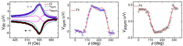
The structural information (X-ray reflectivity and Raman spectroscopy) regarding the samples has been mentioned in the SI. The Gilbert damping parameter () was determined by fitting the resonance field () and linewidth () data from ferromagnetic resonance spectroscopy, as explained in the SI. The (10-3) values of the samples M1-M7 are mentioned in Table I, which are higher than that of the reference layer M0 (8.20.1). The elevated values in the bilayer and trilayer samples suggest the presence of potential spin pumping. However, the contribution of other effects cannot be excluded. To confirm the presence of spin pumping, we conducted ISHE measurements on these samples. Fig. 1(a) displays the variation in the measured voltage caused by ISHE as a function of the applied field H for the sample M5 at in-plane angles () 0 and 180 degrees. The symmetric (Vsym) and antisymmetric (Vasym) components of the measured voltage signal () were separated by fitting the data to the following Lorentzian equation Conca et al. (2017),
| (1) | |||
Here, represents the angle between the direction of the measured voltage and the direction perpendicular to the applied H. The reversal in the sign of as shifts from 0∘ to 180∘ clearly indicates the presence of spin pumping in our samples. In ISHE experiments, the voltage signal detected may also reflect contributions from parasitic spin rectification effects (SREs). SREs arise from the generation of a DC voltage in ferromagnetic layers due to the non-linear coupling between the dynamic resistance R, which depends on the time-varying magnetic field H (t), and the dynamic current I (t). Key factors driving SREs include the anomalous Hall effect (AHE) and anisotropic magnetoresistance (AMR). To obtain the contributions due to AHE and AMR, angle-dependent ISHE measurements were conducted. In Fig. 1(b) and (c), the angle-dependent and components, respectively, for sample M5 are shown. The plots were fitted using the following equations Conca et al. (2017):
| (2) | |||
| (3) | |||
An additional factor has been included to account for the misalignment in sample positioning when defining the values during measurements. Here, is the angle between the electric and magnetic fields of the applied microwave which is 90∘. Different voltage components, as determined from the angle-dependent ISHE measurements, are listed in Table I.
| Sample | (nm) | (V) | (V) | (V) | (V) | (10-3) | (nm-2) |
|---|---|---|---|---|---|---|---|
| M1 | 0 | 2.98 0.08 | 0.18 0.06 | 2.31 0.08 | 0.012 0.001 | 11.40 0.10 | 14.60 0.02 |
| M2 | 0.65 | 0.97 0.02 | 0.32 0.01 | 0.54 0.03 | 0.002 0.001 | 13.60 0.10 | 24.70 0.04 |
| M3 | 2 | 1.68 0.05 | 0.16 0.02 | 1.08 0.06 | 0.13 0.03 | 13.20 0.20 | 27.10 0.03 |
| M4 | 3 | 2.16 0.11 | 0.48 0.04 | 1.53 0.12 | 0.11 0.05 | 13.30 0.10 | 28.30 0.20 |
| M5 | 5 | 5.70 0.12 | 0.49 0.01 | 3.36 0.13 | 0.17 0.06 | 13.01 0.10 | 26.20 0.20 |
| M6 | 7 | 4.45 0.13 | 1.72 0.05 | 2.63 0.13 | 0.28 0.06 | 12.80 0.10 | 25.50 0.30 |
| M7 | 10 | 4.28 0.05 | 1.06 0.04 | 2.77 0.05 | 0.11 0.02 | 12.90 0.20 | 25.27 0.20 |
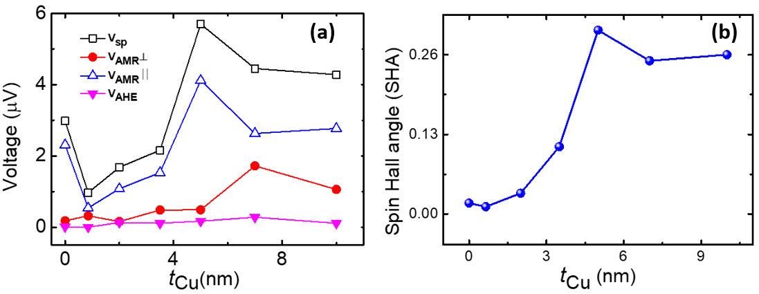
It has been observed that dominates over the rectification effects indicating a strong spin pumping phenomenon as shown in Fig. 2(a). The effective spin mixing conductance, which dictates the amount of spin current that can flow through the interface, was determined using the following expression:
| (4) |
where , , , and g represent the difference in from the reference CoFeB layer, the saturation magnetization, the thickness of the CoFeB layer, the Bohr magneton, and the Landé g-factor, respectively. The measured values for the samples M1-M7 are mentioned in Table-I. The values of in the trilayer structure with Cu are higher compared to the bilayer structure without Cu. This indicates that Cu layer promotes efficient spin transfer across the interface. The values of obtained from SQUID magnetometry for the samples M0-M7 were found to be 801 31, 840 25, 790 36, 833 20, 843 32, 820 34, 848 23 and 818 28 emu/cc, respectively. We evaluated the spin to charge conversion efficiency of the samples, known as the spin Hall angle (), using the following expression Ando et al. (2011):
| (5) |
where is given by,
| (6) |
Here, w represents the transmission linewidth of the coplanar waveguide (CPW), R is the resistance of the samples measured using the four-probe method, and is the spin diffusion length. In our setup, the rf field () is 0.5 Oe, and the transmission line width, w is 200 m. We have considered the spin diffusion length of 7.83 nm from our previous report Mishra et al. (2024). Fig.2 (b) shows the variation of as a function of . shows the maximum value of 0.30±0.01 at the of 5 nm before further decreasing. This value is one order higher than that of MoS2/CoFeB bilayer (sample M1) which is 0.0200.003.
The initial decrease in the could be due to the increased roughness for a 0.65 nm thick Cu layer. At this very thin Cu layer, the finite size effect comes into play Zhou and Gall (2018). This effect arises because, at these small thicknesses, electron scattering at the surfaces and grain boundaries becomes significant, increasing the overall resistivity. The resistance of the samples varies from 3620.45 to 260.09 from sample M1 to M7 which indicates the shunting effect due to Cu. This further means that the electrons in the Cu layer experience more scattering events at low thickness of Cu, including spin-flip scattering, which disrupts the spin alignment and reduces the efficiency of spin transport. As a result, the spin Hall angle decreases initially. With increasing Cu thickness, the Cu layer starts to act as a good spin transmitter with minimal dissipation and reduced spin flipping, preserving the spin polarization. This leads to an increase in the spin Hall angle. When the thickness of the Cu layer increases to 5 nm, the Cu layer becomes thick enough to support spin accumulation. This accumulation refers to the buildup of spin-polarized electrons at the interfaces, which can occur when the layer is thick enough to allow spins to diffuse without significant spin-flip scattering. This suggests that the spin Hall angle of the Cu interlayer generates a positive voltage response Wang et al. (2014), reducing the net spin Hall angle. In the MoS2/CoFeB structure, the direct interface may lead to significant spin dissipation and the formation of mixed electronic states that could hinder efficient spin accumulation. Hence, the Cu interlayer helps decouple these effects, providing an additional cleaner pathway for spin currents to reach the MoS2 layer.
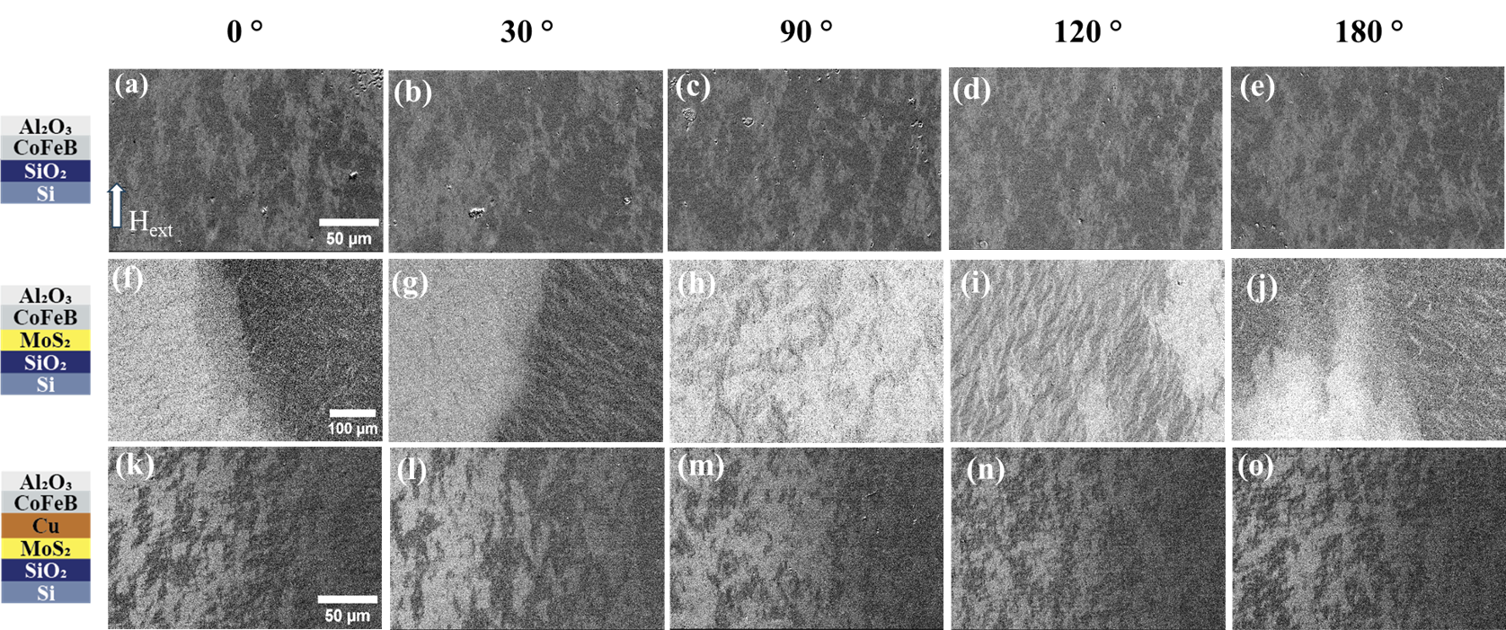
In order to further confirm the decoupling at the MoS2/Cu/CoFeB trilayer, we performed magneto-optic Kerr effect-based microscopy. The domain images presented in Fig. 3. (a-e) indicate the isotropic nature of the reference CoFeB layer (M0). These findings suggest that the CoFeB layer exhibits magnetic isotropy in the film plane, a characteristic commonly observed in amorphous ferromagnets where magnetocrystalline anisotropy is minimal due to the absence of long-range structural order Xie et al. (2020); Nayar and Batra (1990). In contrast, domain images at 0∘ and 180∘ for M1, shown in Fig.3 (f) and (j), reveal large domains, suggesting that magnetization reversal occurs through domain wall nucleation and motion Chowdhury and Bedanta (2014). This implies that MoS2 induces substantial anisotropy in the CoFeB layer. Interestingly, when Cu is inserted as a spacer layer between MoS2 and CoFeB, the magnetic microstructures of CoFeB are now separated from MoS2, as evidenced by the similar domain images to those of the reference CoFeB layer shown in Fig. 3 (k-o). The domain structures for sample M5, exhibit negligible changes. This indicates that the introduction of the Cu layer effectively prevents any proximity-induced effects at the MoS2/CoFeB interface that could disrupt spin transport and conversion efficiency.
IV Theoretical calculations
To understand the role of the Cu spacer layer in the spin-pumping we performed first-principles based calculation to estimate the spin Hall angles (SHA) in MoS2/CoFeB and MoS2/Cu/CoFeB systems within the framework of Density Functional Theory (DFT). The detailed methodology of these calculations is mentioned in the SI. The spin Hall angle is given by Qu et al. (2014),
| (7) |
Where is the spin Hall conductivity (SHC) and is the longitudinal charge conductivity. In the present work, we consider the intrinsic SHE. The SHC was calculated via mapping DFT Hamiltonian to an effective Wannier Hamiltonian using Wannier90 approach and by using Kubo’s formula given by Pizzi et al. (2020); Qiao et al. (2018),
| (8) |
Here summation over is performed over all occupied bands, and N is the number of -points in the first Brillouin zone. is the Fermi-Dirac distribution function. The spin Berry curvature is defined by Pizzi et al. (2020); Qiao et al. (2018),
| (9) |
The longitudinal charge conductivity was calculated using the BOLTZWANN module Pizzi et al. (2014). is the spin-current operator given by
The calculated SHA () for the MoS2/CoFeB is 0.022 while for MoS2/Cu/CoFeB the corresponding value is 0.043. This supports the experimental claim that Cu effectively decouples MoS2 from the magnetic exchange interaction with CoFeB, preserving the spin-orbit coupling (SOC) properties of MoS2. Our theoretical results further validate the assertion that the intrinsic SHE, a key mechanism for spin-charge conversion in such systems, is augmented by interfacial modifications.
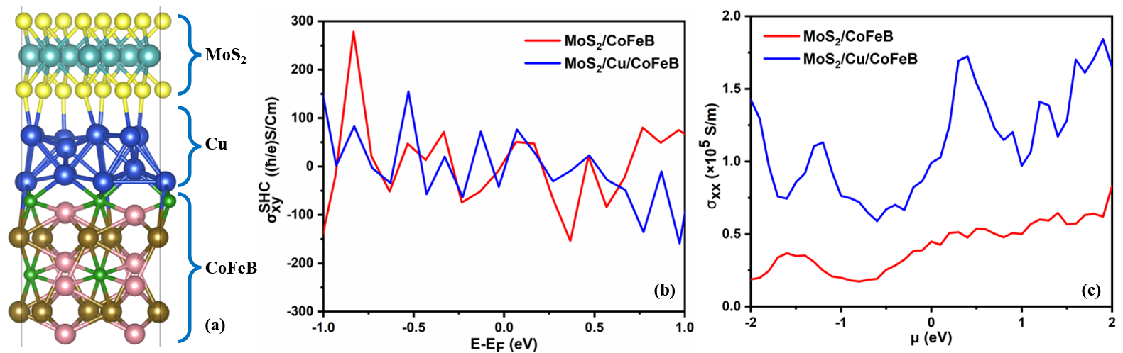
In Fig.4(a) we show the atomic structure of the MoS2/Cu/CoFeB heterostructure under consideration, while in the Fig.4 (b) we plot the spin Hall conductivity () as a function of energy relative to the Fermi energy () for the two configurations. The red curve represents the MoS2/CoFeB system, while the blue curve corresponds to the MoS2/Cu/CoFeB system. Both curves exhibit oscillatory behavior, but the blue curve shows more periodic peaks than the red curve. In Fig.4 (c) we show the longitudinal charge conductivity () is plotted as a function of the chemical potential () for the two configurations.
From the denominator of Eq. 9, it is evident that peaks in the spin Hall conductivity (Fig. 4(b)) are associated with avoided crossings in the band structure near the Fermi level, which directly influence the spin Berry curvature due to spin-orbit coupling (SOC) effects. In the MoS2/CoFeB system, proximity-induced exchange interactions at the interface modify the electronic structure of MoS2, partially suppressing its intrinsic SOC. The irregular peaks in the spin Hall conductivity suggest that the SOC effect is non-uniform and influenced by CoFeB’s magnetic properties. Introducing a Cu interlayer between MoS2 and CoFeB decouples MoS2 from these magnetic interactions, resulting in more symmetric peaks in the spin Berry curvature for the MoS2/Cu/CoFeB system. This results in enhanced spin Hall conductivity and reduced interfacial scattering in the Cu-intercalated system. This can be further understood by our calculation of magnetic anisotropy energy (MAE). Indeed, our calculated MAE values strongly support the discussion of spin Berry curvature and spin Hall conductivity behavior. The higher MAE for the MoS2/Cu/CoFeB (9.83106 erg/cm3) system compared to MoS2/CoFeB (7.2106 erg/cm3) aligns well with the enhanced preservation of SOC and reduced proximity-induced effects in the Cu-intercalated structure. This increased anisotropy reflects the effectiveness of the Cu-interlayer in decoupling MoS2 from CoFeB, allowing MoS2’s intrinsic properties to dominate. Such consistency between MAE calculations and spin transport properties further ensures the importance of interface engineering for optimizing spintronic device performance.
V Conclusion
We demonstrated a significantly enhanced spin-to-charge conversion efficiency, increased by an order of magnitude, through Cu intercalation in the MoS2/CoFeB system. Domain imaging revealed that Cu effectively decouples MoS2 from proximity effects with CoFeB. These experimental results are further supported by theoretical calculations using the DFT-WANNIER90 framework, which show notable improvements in spin Berry curvature, spin Hall conductivity, and magnetic anisotropy energy. Using the first-principles based calculations, we demonstrate that Cu intercalation preserves the intrinsic SOC of MoS2 by decoupling it from CoFeB’s magnetic exchange interactions, leading to a significant enhancement in the spin Hall effect. Our findings may pave the way for the development of highly efficient spintronic devices by leveraging intercalation strategies to engineer material interfaces.
VI Acknowledgments
AM, RC, SD, SS, KSR, and S. Bedanta thank the Department of Atomic Energy (DAE), Government of India, for the financial support via project with Sanct. No. 0803/2/2020/NISER/R&D-II/8149 dated 16.07.2021). The authors acknowledge SERB project (CRG/2021/001245 dated 05.03.2022) for financial assistance.
References
- Hirohata et al. (2020) A. Hirohata, K. Yamada, Y. Nakatani, I.-L. Prejbeanu, B. Diény, P. Pirro, and B. Hillebrands, Journal of Magnetism and Magnetic Materials 509, 166711 (2020).
- Soumyanarayanan et al. (2016) A. Soumyanarayanan, N. Reyren, A. Fert, and C. Panagopoulos, Nature 539, 509 (2016).
- Ryu et al. (2020) J. Ryu, S. Lee, K.-J. Lee, and B.-G. Park, Advanced Materials 32, 1907148 (2020).
- Tserkovnyak et al. (2002) Y. Tserkovnyak, A. Brataas, and G. E. Bauer, Physical Review B 66, 224403 (2002).
- Hirsch (1999) J. Hirsch, Physical review letters 83, 1834 (1999).
- Saitoh et al. (2006) E. Saitoh, M. Ueda, H. Miyajima, and G. Tatara, Applied physics letters 88 (2006).
- Roy et al. (2021) K. Roy, A. Mishra, P. Gupta, S. Mohanty, B. B. Singh, and S. Bedanta, Journal of Physics D: Applied Physics 54, 425001 (2021).
- Singh et al. (2020) B. B. Singh, K. Roy, J. A. Chelvane, and S. Bedanta, Physical Review B 102, 174444 (2020).
- Singh and Bedanta (2020) B. B. Singh and S. Bedanta, Physical Review Applied 13, 044020 (2020).
- Kimata et al. (2019) M. Kimata, H. Chen, K. Kondou, S. Sugimoto, P. K. Muduli, M. Ikhlas, Y. Omori, T. Tomita, A. H. MacDonald, S. Nakatsuji, et al., Nature 565, 627 (2019).
- Singh et al. (2019) B. B. Singh, S. K. Jena, M. Samanta, K. Biswas, B. Satpati, and S. Bedanta, physica status solidi (RRL)–Rapid Research Letters 13, 1800492 (2019).
- Jamali et al. (2015) M. Jamali, J. S. Lee, J. S. Jeong, F. Mahfouzi, Y. Lv, Z. Zhao, B. K. Nikolic, K. A. Mkhoyan, N. Samarth, and J.-P. Wang, Nano letters 15, 7126 (2015).
- Sierra et al. (2021) J. F. Sierra, J. Fabian, R. K. Kawakami, S. Roche, and S. O. Valenzuela, Nature Nanotechnology 16, 856 (2021).
- Liu et al. (2020) Y. Liu, C. Zeng, J. Zhong, J. Ding, Z. M. Wang, and Z. Liu, Nano-Micro Letters 12, 1 (2020).
- Kumar and Panda (2022) V. P. Kumar and D. K. Panda, ECS Journal of Solid State Science and Technology 11, 033012 (2022).
- Choi et al. (2017) W. Choi, N. Choudhary, G. H. Han, J. Park, D. Akinwande, and Y. H. Lee, Materials Today 20, 116 (2017).
- Akinwande et al. (2014) D. Akinwande, N. Petrone, and J. Hone, Nature communications 5, 5678 (2014).
- Xie et al. (2019) Q. Xie, W. Lin, B. Yang, X. Shu, S. Chen, L. Liu, X. Yu, M. B. Breese, T. Zhou, M. Yang, et al., Advanced Materials 31, 1900776 (2019).
- Thiruvengadam et al. (2022) V. Thiruvengadam, A. Mishra, S. Mohanty, and S. Bedanta, ACS Applied Nano Materials 5, 10645 (2022).
- Mishra et al. (2024) A. Mishra, P. Gupta, V. Thiruvengadam, B. B. Singh, and S. Bedanta, Journal of Alloys and Compounds 970, 172076 (2024).
- Mendes et al. (2018) J. Mendes, A. Aparecido-Ferreira, J. Holanda, A. Azevedo, and S. Rezende, Applied Physics Letters 112 (2018).
- Husain et al. (2018) S. Husain, A. Kumar, P. Kumar, A. Kumar, V. Barwal, N. Behera, S. Choudhary, P. Svedlindh, and S. Chaudhary, Physical Review B 98, 180404 (2018).
- Bansal et al. (2019) R. Bansal, A. Kumar, N. Chowdhury, N. Sisodia, A. Barvat, A. Dogra, P. Pal, and P. Muduli, Journal of Magnetism and Magnetic Materials 476, 337 (2019).
- Du et al. (2014) C. Du, H. Wang, F. Yang, and P. C. Hammel, Physical Review Applied 1, 044004 (2014).
- Longo et al. (2021) E. Longo, L. Locatelli, M. Belli, M. Alia, A. Kumar, M. Longo, M. Fanciulli, and R. Mantovan, Advanced Materials Interfaces 8, 2101244 (2021).
- Zhang et al. (2015) W. Zhang, M. B. Jungfleisch, W. Jiang, J. E. Pearson, and A. Hoffmann, Journal of Applied Physics 117 (2015).
- Yakata et al. (2006) S. Yakata, Y. Ando, T. Miyazaki, and S. Mizukami, Japanese journal of applied physics 45, 3892 (2006).
- Conca et al. (2017) A. Conca, B. Heinz, M. Schweizer, S. Keller, E. T. Papaioannou, and B. Hillebrands, Physical Review B 95, 174426 (2017).
- Ando et al. (2011) K. Ando, S. Takahashi, J. Ieda, Y. Kajiwara, H. Nakayama, T. Yoshino, K. Harii, Y. Fujikawa, M. Matsuo, S. Maekawa, et al., Journal of applied physics 109 (2011).
- Zhou and Gall (2018) T. Zhou and D. Gall, Physical Review B 97, 165406 (2018).
- Wang et al. (2014) H. Wang, C. Du, Y. Pu, R. Adur, P. C. Hammel, and F. Yang, Physical review letters 112, 197201 (2014).
- Xie et al. (2020) Y. Xie, Q. Zhan, Y. Hu, X. Hu, X. Chi, C. Zhang, H. Yang, W. Xie, X. Zhu, J. Gao, et al., NPG Asia Materials 12, 67 (2020).
- Nayar and Batra (1990) P. Nayar and I. Batra, Journal of magnetism and magnetic materials 87, 357 (1990).
- Chowdhury and Bedanta (2014) N. Chowdhury and S. Bedanta, AIP advances 4 (2014).
- Qu et al. (2014) D. Qu, S. Huang, B. Miao, S. Huang, and C. Chien, Physical Review B 89, 140407 (2014).
- Pizzi et al. (2020) G. Pizzi, V. Vitale, R. Arita, S. Blügel, F. Freimuth, G. Géranton, M. Gibertini, D. Gresch, C. Johnson, T. Koretsune, et al., Journal of Physics: Condensed Matter 32, 165902 (2020).
- Qiao et al. (2018) J. Qiao, J. Zhou, Z. Yuan, and W. Zhao, Physical Review B 98, 214402 (2018).
- Pizzi et al. (2014) G. Pizzi, D. Volja, B. Kozinsky, M. Fornari, and N. Marzari, Computer Physics Communications 185, 422 (2014).