A Prototype-Based Framework to Design Scalable Heterogeneous SoCs with Fine-Grained DFS ††thanks: This work was partly funded by the ISOLDE project (Grant No. 101112274), supported by CHIPS Joint Undertaking.
Abstract
Frameworks for the agile development of modern system-on-chips are crucial to dealing with the complexity of designing such architectures. The open-source Vespa framework for designing large, FPGA-based, multi-core heterogeneous system-on-chips enables a faster and more flexible design space exploration of such architectures and their run-time optimization. Vespa, built on ESP, introduces the capabilities to instantiate multiple replicas of the same accelerator in a single network-on-chip node and to partition the system-on-chips into frequency islands with independent dynamic frequency scaling actuators, as well as a dedicated run-time monitoring infrastructure. Experiments on 4-by-4 tile-based system-on-chips demonstrate the possibility of effectively exploring a multitude of solutions that differ in the replication of accelerators, the clock frequencies of the frequency islands, and the tiles’ placement, as well as monitoring a variety of statistics related to the traffic on the interconnect and the accelerators’ performance at run time.
I Introduction
While general-purpose central processing units (CPUs) transitioned to multi- and many-core architectures in the last decades, due to the slowdown in the improvement of their performance and efficiency with the end of Moore’s law and Dennard scaling, hardware acceleration emerged as the standard solution to support modern computationally intensive workloads ranging from cryptography [1] to deep-learning [2] ones.
The increased complexity and development costs of system-on-chips (SoCs), that are commonly heterogeneous multi-core processors combining general-purpose CPU cores and hardware accelerators, including those obtained through high-level synthesis (HLS) [3], have imposed the research and the adoption of novel design methods for their architectural exploration, system integration, verification, validation, and physical design. Agile development through field-programmable gate array (FPGA)-based prototyping has therefore emerged as the standard paradigm to support the rapid design of complex heterogeneous platforms, offering a complementary tool to classic cycle-accurate simulators. For this reason, a multitude of frameworks to quickly deliver FPGA prototypes has been introduced during the last decade, fueled by a drop in the cost per look-up table and by the availability of ever-larger FPGAs.
While cycle-accurate simulators were traditionally used in the early stages of the architectural exploration, the specialization of the current computing platforms has hindered their adoption. They fail indeed to support the accurate simulation of complex computing platforms with hardware accelerators since the employed generic area and power models cannot provide accurate estimates, whereas designing area and power simulation models for each specific accelerator is a lengthy and difficult process. In addition, simulators’ performance is severely curbed by their single-thread software architecture.
Enabling a quick and comprehensive design space exploration (DSE) of such complex architectures, also accounting for their run-time optimization, is critical, and even the few available open-source frameworks [4, 5, 6] lack such support. Indeed, the ESP [4] state-of-the-art framework for the agile development of complex accelerator-centric multi-core heterogeneous SoCs notably combines a scalable tile-based architecture and a flexible system-level design methodology to deliver prototypes on FPGA targets, but its tiles’ limited configurability prevents an in-depth DSE and it lacks the dynamic frequency scaling (DFS) actuators and a proper run-time monitoring infrastructure required to support an effective run-time optimization [7].
Contributions
This work introduces the Vespa framework, which extends ESP [4] to enable both the DSE and the run-time optimization of large multi-core heterogeneous SoCs, providing three main contributions.
-
1.
A design-time parameter and related hardware infrastructure enable scaling the throughput of third-party hardware accelerators, without altering the design of the latter or the network-on-chip (NoC) interconnect, by instantiating multiple replicas of the same accelerator within a single computing tile assigned to an NoC node,
-
2.
The on-chip interconnect and the computing elements can be configurably partitioned into frequency islands, each of whom is independent from the others and is fed a clock signal that is either fixed or generated by a DFS actuator.
-
3.
A run-time monitoring infrastructure enables the collection of various execution statistics, exposed through memory-mapped hardware counters, to support the DSE and the run-time optimization of the SoC.
The Vespa framework for the design space exploration and run-time optimization of large multi-core heterogeneous SoCs is publicly available and released open source111https://github.com/hardware-fab/vespa. with the goal of fostering further research in the field.
II Methodology
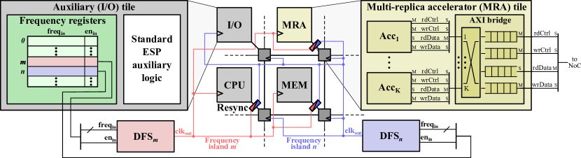
The Vespa framework, depicted in Figure 1, leverages ESP and enables the design space exploration and run-time optimization of complex accelerator-based SoCs by means of flexible multi-replica accelerator tiles, configurable-DFS frequency islands, and a dedicated run-time monitoring infrastructure.
II-A Multi-replica accelerator-tile architecture
A simple and time-efficient solution to increase the throughput of an existing hardware accelerator integrated into a computing platform is to instantiate multiple replicas of the former. Indeed, instantiating K such replicas intuitively provides a K× increase of the throughput of the baseline accelerator.
Vespa’s multi-replica accelerator tiles (MRA in Figure 1) can instantiate multiple replicas (Acci) of a hardware accelerator within a single computing tile without any changes either to the accelerator or the size and topology of the NoC interconnect, and avoiding being forced to occupy multiple computing tiles with the same accelerator in order to improve its performance. The multi-replica accelerator tiles support any third-party hardware accelerator that exposes an AXI interface. Their replication factor K, which corresponds to the number of copies of an accelerator that are instantiated and operate in parallel, is configurable by the system designer to easily tune the trade-off between throughput and area.
A baseline accelerator to be integrated into an ESP SoC exposes four AXI4-Stream interfaces for read control (rdCtrl), write control (wrCtrl), read data (rdData), and write data (wrData) purposes, respectively. A multi-replica accelerator tile still exposes the same AXI4-Stream interfaces towards the NoC interconnect (NoC) to guarantee full compatibility with the ESP SoC architecture. The AXI bridge component is therefore tasked with multiplexing the four AXI4-Stream interfaces of each of the K accelerator replicas into four corresponding buffers for the AXI4-Stream interfaces of the tile.
II-B Configurable-DFS frequency-island architecture
The Vespa framework allows partitioning the SoC into multiple frequency islands at design time. Every SoC tile and NoC router is assigned to a frequency island that can group multiple computing and routing elements. Each frequency island is fed an independent clock signal that can either have a fixed frequency or be generated by a dedicated DFS actuator.
The architecture supporting such SoC partitioning can be split into three main components, namely a set of registers holding the frequency configuration of each island (Frequency registers in Figure 1), a DFS actuator (DFS) for each of the frequency islands, and resynchronizers (Resync) at the boundaries of the latter.
Notably, the clock signal output by the mixed-mode clock managers (MMCMs) of an AMD FPGA remains low during its reconfiguration, thus causing a clock-gating effect on the computing platform. The DFS actuator implemented in the Vespa framework avoids such negative effect by employing two MMCM components. In each DFS actuator, an internal finite-state machine forces the master MMCM to preserve the current output clock signal while the slave one is under reconfiguration, after which their roles are swapped.
| Baseline (1×) accelerator | 2×-replication instance | 4×-replication instance | |||||||||||||
| Accel. | LUT | FF | BRAM | DSP | Thr. | LUT | FF | BRAM | DSP | Thr. | LUT | FF | BRAM | DSP | Thr. |
| adpcm | 10899 | 11720 | 25 | 81 | 1.40 | 16455 | 15158 | 48 | 162 | 2.76 | 27313 | 21780 | 94 | 324 | 5.41 |
| dfadd | 11268 | 11199 | 2 | 9 | 9.22 | 16988 | 14090 | 2 | 18 | 16.88 | 28599 | 19614 | 2 | 36 | 26.06 |
| dfmul | 8435 | 10222 | 2 | 25 | 8.70 | 11352 | 12136 | 2 | 50 | 15.07 | 17382 | 15706 | 2 | 100 | 26.06 |
| dfsin | 16627 | 14997 | 2 | 52 | 0.33 | 27770 | 21686 | 2 | 104 | 0.65 | 50043 | 34804 | 2 | 208 | 1.24 |
| gsm | 9900 | 11418 | 18 | 62 | 4.61 | 14304 | 14520 | 34 | 124 | 8.90 | 22927 | 20473 | 66 | 248 | 16.67 |
| Incr. | 1.50× | 1.29× | 1.36× | 2.00× | 1.89× | 2.49× | 1.85× | 2.09× | 4.00× | 3.41× | |||||
II-C Run-time monitoring infrastructure
Vespa’s run-time monitoring infrastructure is crucial to collecting statistics from the computing platform and thus supporting run-time optimization policies and design space exploration. For each accelerator, the run-time monitoring infrastructure can selectively enable the monitoring of up to four different statistics, each corresponding to a specific counter in the tile: execution time, number of incoming and outgoing packets, and the round-trip time. The latter is defined as the time occurring between a request for data from an accelerator to the main memory through direct memory access and the ensuing arrival of such data to the accelerator.
The execution time counter automatically resets when the accelerator tile starts its computation and stops when the latter is completed, while the other three counters are reset manually. All counters instantiated on accelerator tiles expose memory-mapped registers that can be accessed both via software executing on CPU cores of the SoC itself and via the USB-to-serial interface that connects the platform to the host.
III Experimental evaluation
The experimental campaign targeted a Siemens proFPGA quad (mb-4m-r3) motherboard222https://www.profpga.com/products/motherboards-overview/profpga-quad equipped with a Virtex-7 2000 FPGA (fm-xctv2000t-r2) module333https://www.profpga.com/products/fpga-modules-overview/virtex-7-based/profpga-xc7v2000t, whose AMD FPGA chip features 1221600 look-up tables (LUT), 2443200 flip-flops (FF), 2584 18Kb blocks of block RAM (BRAM), 2160 digital signal processing (DSP) elements, and 24 MMCMs.
The accelerators instantiated in the SoC were obtained through HLS of applications from the CHStone benchmark suite [8]. We employed Cadence Xcelium 20.09 to simulate SoC instances, AMD Vivado 2019.2 for HLS, RTL synthesis and implementation, and bitstream generation, and Siemens proFPGA Builder 2019A-SP2 for FPGA programming. Area and timing results refer to the post-implementation netlists of the prototypes, while system-level statistics from the SoC execution are collected from the prototyped SoCs through the run-time monitoring infrastructure described in Section II.
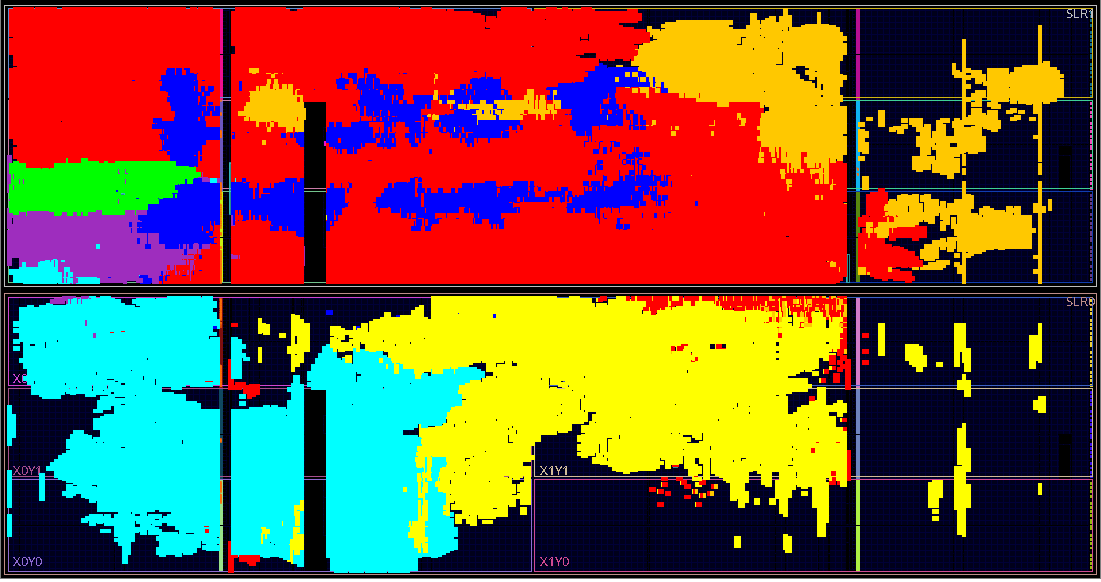
Without loss of generality, we evaluated our methodology on 4-by-4 tile-based SoC instances that feature a CVA6 [9] CPU tile, a DDR memory one, and an auxiliary tile, while the thirteen remaining tiles instantiate HLS-generated CHStone accelerators. Eleven TG tiles generate traffic in the NoC interconnect and implement dfadd accelerators, which were empirically observed to be memory-bound, and two more accelerator tiles are placed in the A1 and A2 positions, that are respectively close to (A1) and far from (A2) memory (MEM). The SoC is split into five separate frequency islands, namely, the A1 and A2 accelerators, the NoC interconnect and memory controller (MEM), the traffic generation (TG) cores, the CPU core (CPU), and the auxiliary tile (I/O). The DFS actuator of the NoC island implements a range of operating frequencies comprised between 10MHz and 100MHz, while the other four clock domains support clock signals with frequencies from 10MHz to 50MHz. The clock frequency ranges include values at 5MHz steps. Figure 2 depicts the FPGA floorplan of an SoC instance.
III-A Multi-replica accelerator tiles: area-performance analysis
Each baseline HLS-generated accelerator occupies up to 1.4%, 0.6%, 1.0%, and 3.8% of the LUT, FF, BRAM, and DSP resources available on the target FPGA, as listed in Table I, thus justifying the possibility to improve their performance by exploiting the multi-replica accelerator-tile architecture. We explore therefore the instantiation of 2×- and 4×-replication tiles and compare their resource utilization and throughput. The throughput is measured on the accelerator instantiated in the A1 tile, with clock frequencies of 100MHz and 50MHz for the NoC-MEM and A1-tile islands, respectively, and with all TG tiles disabled, thus providing the best performance achievable by the accelerator due to its proximity to memory and no concurrent requests from the other computing tiles in the SoC.
The increase of LUT, FF, and BRAM utilization is shown to be quite smaller than the replication factor, since such resources are also being employed in the additional logic of the multi-replica accelerator tile. On the contrary, DSP resources end up being around 2 and 4 times as much as in the baseline versions. Performance also scales correspondingly with the replication of accelerators, as shown by the throughput columns in TABLE I. The 2×- and 4×-replication tiles have an average throughput increase of 1.92× and 3.58×, respectively. The larger average throughput improvement compared to the corresponding increase in LUT, FF, and BRAM utilization justifies our multi-replica accelerator-tile solution.
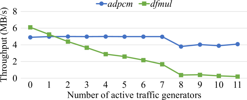
III-B SoC accelerators: performance analysis
We select adpcm and dfmul as representative examples of compute- and memory-bound accelerators, respectively, and analyze the relation between their throughput and the amount of traffic in the NoC interconnect generated by TG cores. Figure 3 depicts the throughput of the adpcm and dfmul accelerators with a number of active TG cores ranging between 0, i.e., when all of them are disabled, and 11, i.e., when all the TG cores in the SoC are enabled. The NoC interconnect runs at 10MHz while the accelerators and TG cores operate at 50MHz.
The compute-bound adpcm shows an almost constant throughput between 0 and 7 active TG cores while, on the contrary, in the same range of X axis values, the throughput of the dfmul accelerator drastically decreases, thus highlighting the memory-bound nature of the latter.
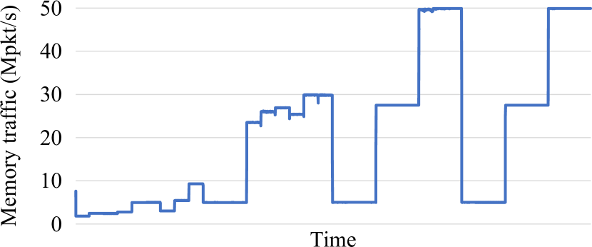
III-C Memory: traffic analysis
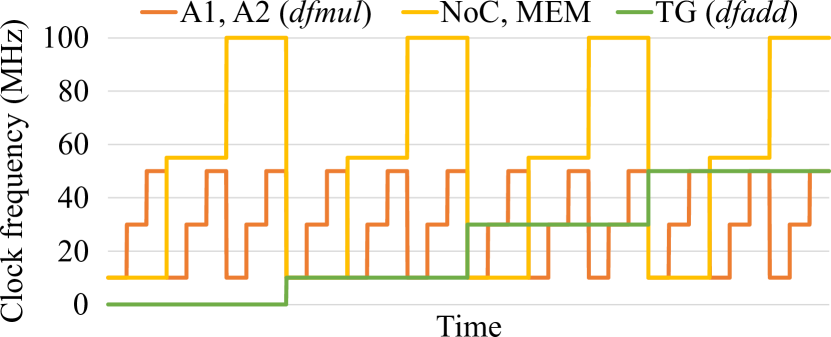
Finally, we show the possibility of evaluating the memory traffic depending on the clock frequencies of the various frequency islands. We consider a specific SoC instance with A1 and A2 tiles both instantiating the memory-bound dfmul and running concurrently. Figure 4 depicts the temporal evolution of incoming data packets to memory, expressed as millions of packets per second (Mpkt/s) in Figure 4(b), while varying the frequency islands’ clock frequencies, depicted in Figure 4(a) in red for the A1 and A2 tiles, yellow for the NoC interconnect and memory controller, and green for the TG cores.
Varying the clock frequency of the A1 and A2 tiles between 10MHz, 30MHz, and 50MHz values is shown to have a negligible impact on the memory incoming traffic, while increasing the operating frequency of the TG cores drastically increases the pressure on memory when the NoC interconnect and memory controller are also running at a high clock frequency. Such results demonstrate the possibility to analyze the impact of DFS on the local and global traffic of the SoC.
IV Conclusions
This paper introduced the open-source Vespa framework for designing large tile-based multi-core heterogeneous SoCs. Vespa extends the open-source ESP toolchain by i) adding the possibility to configure the area-performance trade-off for each accelerator tile, ii) partitioning the SoC into multiple frequency islands with independent true DFS actuators, and iii) implementing a run-time monitoring infrastructure that enables the DSE of complex prototypes.
The experimental campaign, targeting a large AMD Virtex-7 2000 FPGA chip, demonstrated its effectiveness in analyzing the area-performance trade-off by leveraging the scalable throughput architecture, the DFS actuators, and the run-time monitoring infrastructure, thus making the proposed framework a valuable tool for designing large FPGA-based systems.
References
- [1] A. Galimberti, D. Galli, G. Montanaro, W. Fornaciari, and D. Zoni, “Fpga implementation of bike for quantum-resistant tls,” in 2022 25th Euromicro Conference on Digital System Design (DSD), 2022, pp. 539–547.
- [2] Y.-H. Chen, T. Krishna, J. S. Emer, and V. Sze, “Eyeriss: An energy-efficient reconfigurable accelerator for deep convolutional neural networks,” IEEE Journal of Solid-State Circuits, vol. 52, no. 1, pp. 127–138, 2017.
- [3] A. Galimberti, G. Montanaro, and D. Zoni, “Hls-based acceleration of the bike post-quantum kem on embedded-class heterogeneous socs,” in 2023 30th IEEE International Conference on Electronics, Circuits and Systems (ICECS), 2023, pp. 1–4.
- [4] P. Mantovani, D. Giri, G. Di Guglielmo, L. Piccolboni, J. Zuckerman, E. G. Cota, M. Petracca, C. Pilato, and L. P. Carloni, “Agile soc development with open esp,” in Proceedings of the 39th International Conference on Computer-Aided Design, 2020, pp. 1–9.
- [5] A. Amid, D. Biancolin, A. Gonzalez, D. Grubb, S. Karandikar, H. Liew, A. Magyar, H. Mao, A. Ou, N. Pemberton et al., “Chipyard: Integrated design, simulation, and implementation framework for custom socs,” IEEE Micro, vol. 40, no. 4, pp. 10–21, 2020.
- [6] J. Balkind, T.-J. Chang, P. J. Jackson, G. Tziantzioulis, A. Li, F. Gao, A. Lavrov, G. Chirkov, J. Tu, M. Shahrad, and D. Wentzlaff, “Openpiton at 5: A nexus for open and agile hardware design,” IEEE Micro, vol. 40, no. 4, p. 22–31, jul 2020. [Online]. Available: https://doi.org/10.1109/MM.2020.2997706
- [7] D. Zoni, A. Galimberti, and W. Fornaciari, “A survey on run-time power monitors at the edge,” ACM Comput. Surv., vol. 55, no. 14s, jul 2023. [Online]. Available: https://doi.org/10.1145/3593044
- [8] Y. Hara, H. Tomiyama, S. Honda, H. Takada, and K. Ishii, “Chstone: A benchmark program suite for practical c-based high-level synthesis,” in 2008 IEEE International Symposium on Circuits and Systems (ISCAS), 2008, pp. 1192–1195.
- [9] F. Zaruba and L. Benini, “The cost of application-class processing: Energy and performance analysis of a linux-ready 1.7-ghz 64-bit risc-v core in 22-nm fdsoi technology,” IEEE Transactions on Very Large Scale Integration (VLSI) Systems, vol. 27, no. 11, pp. 2629–2640, Nov 2019.