Scalable Wavelength Arbitration for Microring-based DWDM Transceivers
Abstract
This paper introduces the concept of autonomous microring arbitration, or wavelength arbitration, to address the challenge of multi-microring initialization in microring-based Dense-Wavelength-Division-Multiplexed (DWDM) transceivers. This arbitration is inherently policy-driven, defining critical system characteristics such as the spectral ordering of microrings. Furthermore, to facilitate large-scale deployment, the arbitration algorithms must operate independently of specific wavelength information and be resilient to system variability. Addressing these complexities requires a holistic approach that encompasses the entire system, from device-level variabilities to the transceiver interface—this system-wide perspective is the focus of this paper. To support efficient analysis, we develop a hierarchical framework incorporating an ideal, wavelength-aware arbitration model to examine arbitration failures at both the policy and algorithmic levels. The effectiveness of this approach is demonstrated in two ways: by analyzing the robustness of each policy in relation to device variabilities, and by developing an algorithm that achieves near-perfect alignment with the ideal model, offering superior robustness compared to the traditional sequential tuning method. The simulator code used in this paper is available at https://github.com/wdmsim/wdm-simulator.
Index Terms:
Microring resonator, silicon photonics, wavelength division multiplexing (WDM), WDM receiver, optical interconnects, integrated optoelectronics, thermal tuning.I Introduction
With the overarching demand for bandwidth and the maturation of silicon photonics technology, the next phase for microring-based DWDM transceiver technology targets large-scale deployment, leveraging its high-bandwidth and low-latency characteristics [1, 2, 3, 4, 5, 6]. However, scaling up poses significant challenges in system design, particularly with regard to mass deployment scenarios. A cost-efficient, robust solution is essential, ideally equipped with a comprehensive analytical toolkit for large-scale deployment [7, 8, 9]. For microring-based DWDM transceivers, one major challenge is aligning microring resonances with laser wavelengths—a problem of initialization [10]—which requires judicious arbitration of the microrings to be cost-efficient, robust and autonomous.
Microring resonance control, a common technique for addressing microring initialization [11, 12, 13, 14, 15, 16], involves sweeping the microring resonance across the tuning range and identifying the resonance alignment. For a single microring with a laser tone, the resonance alignment is identified by the peak in intra-cavity optical power (wavelength search) [11, 12, 13], followed by a feedback loop that stabilize the resonance wavelength (wavelength lock) [14, 15, 16]. However, in DWDM systems, the wavelength search would yield multiple peaks due to the multi-wavelength laser, necessitating an “informed” decision to guarantee maximum wavelength allocation [17]; we will call this wavelength arbitration.
Previous work has focused on circuit-level architectures [17, 18, 19, 20, 21], system-level tradeoffs [7, 22, 23] and wavelength allocation algorithms [24, 25, 26], addressing specific aspects of arbitration. To achieve a scalable arbitration system, we introduce a hierarchical framework for wavelength arbitration. In our framework, arbitration is fundamentally policy-driven, with policies defining the wavelength interface of the DWDM transceiver. The implementing algorithm and supporting circuit-level architecture then operate according to these policies. The primary function of arbitration, therefore, is to effectively coordinate microrings while accounting for device-level variations and system-wide constraints, ensuring both robustness and autonomy. While this holistic view is desirable, the challenge lies in efficiently integrating these policies with scalable algorithms and architectures to maintain optimal system performance under varying conditions.
To address this, we introduce an arbitration model to decouple the analysis of policy and algorithm. This model has two components: an ideal, wavelength-aware model and a wavelength-oblivious model. The ideal model evaluates the arbitration policy under the assumption of wavelength-awareness, ensuring policies are effective and well-defined. In contrast, the wavelength-oblivious model evaluates the algorithm under practical conditions, where conflict resolution and wavelength allocation are performed without specific wavelength information. This approach allows us to evaluate arbitration robustness by analyzing failure probabilities across policies and algorithms, while also developing an algorithm that aligns closely with the ideal model, achieving scalability and robustness for high-volume deployment.
This paper is organized as follows. We begin with an overview of the system model in Section II and provide a formal definition of robustness metrics in Section III. Section IV compares different arbitration policies and investigates system-level tradeoffs. Section V presents our proposed arbitration algorithm and compares it with the baseline sequential tuning scheme. Section VI concludes the paper.
II Generalized Wavelength-Domain Model for Wavelength Arbitration
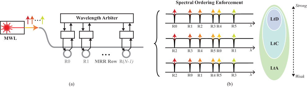
Fig. 1(a) shows the model of wavelength arbitration used in this paper. We assume a typical DWDM transceiver architecture [2] where a multi-wavelength laser propagates into a shared waveguide bus and to downstream microring resonators. During transceiver initialization, each microring captures one of the light wavelengths within its tuning range. This paper focuses on microring wavelength management at initialization, which is represented by the wavelength arbiter in Fig. 1(a). For simplicity, the wavelength initialization process is projected onto the wavelength space; thus, only the wavelength domain is considered throughout the paper.
II-A Wavelength Arbiter
In a typical microring-based DWDM transceiver, the local wavelength status is tracked and updated by the per-microring tuner and sensor circuit [8, 3, 4]. We define the wavelength arbiter as an entity responsible for global wavelength management, maintaining the global wavelength status and overseeing the coordination of the microrings. The outcome of wavelength arbitration is determined by policy, while we define algorithm as the detailed steps to achieve this outcome. For clarity, the algorithm discussed in this paper is wavelength-oblivious; it can access and update the local wavelength status only through the per-microring tuner and sensor.
To explain policy, we first describe the role of microring resonance wavelength in PHY-level data transmission. Just as a port serves a transmission point in the spatial domain, a microring acts as a port in the wavelength-domain. For instance, assume an electrical transmit lane drives a microring at wavelength , and on the receive side, another microring at resonance wavelength is connected to an electrical receive lane. When the host sends packet through the electrical transmit lane, it is retransmitted optically at wavelength , and received by the receive microring, reaching the client side. Thus, optical connectivity for is determined by wavelength , serving as a virtual optical lane for data transmission.
In the context of DWDM, microring spectral ordering can be understood as optical lane ordering (or equivalently, optical port mapping). From a communication standpoint, the transmitting and receiving endpoints should agree on the data ordering. In microring-based DWDM systems, it is preferred that they are cognizant of optical lane ordering during electrical-to-optical and optical-to-electrical conversions111One may argue that bit orderings at both endpoints are handled at MAC-level serialization and deserialization. However, from a transceiver perspective, it is useful to keep track of on-the-fly lane ordering, especially for low-latency applications [27].. We assume an optical port remapper (bit-shuffler backend in Georgas et al. [22]) at the optical transceiver backend to ensure the electrical interfaces at both ends see identical ordering and streamline the data communication. The level of remapping, proportional to the power and latency cost of the backend, is determined by the enforcement level over the microring spectral ordering post-arbitration. In this paper, we adopt the enforcement level as an arbitration policy.
II-B Arbitration Policy
As shown in Fig. 1(b), we consider three wavelength arbitration policies: Lock-to-Deterministic (LtD), Lock-to-Cyclic (LtC) and Lock-to-Any (LtA), each corresponding to strong, medium and weak ordering enforcement, respectively.
LtD policy demonstrates the strongest enforcement on the post-arbitration microring spectral ordering. For example, if the target microring spectral ordering is specified, the arbiter pairs microrings with laser wavelengths in that exact order and disallows any other spectral orderings. By assigning microrings to a predetermined spectral ordering, it can effectively preserve optical lane ordering, bypassing any issues of optical lane shuffling. Spectral-domain link optimization techniques can be applied more easily, such as inter-microring crosstalk minimization [28]. However, despite its apparent advantages, it is challenging to implement due to high microring tuning range requirements, as we will show in Section IV.
LtC policy relaxes the enforcement by allowing cyclic equivalents of the specified target spectral ordering. For example, if the target microring spectral ordering is specified as in Fig. 1, the arbiter can assign microring wavelengths in cyclic equivalents of the ordering, such as , . The required microring tuning range is smaller than that of the LtD policy. This is because a linear shift in spectral ordering effectively cancels any global offsets in laser and microring wavelengths due to ring resonance periodicity222Assume R0, R1, R2, R3 with \qty4\nano FSR are assigned to \qtylist1300;1301;1302;1303\nano laser wavelengths in the order. Due to resonance periodicity by FSR, microrings assigned to \qtylist1301;1302;1303;1304\nano (shift-by-1 order) effectively shift wavelengths by \qty1\nano. [22, 23]. Optical port remapping can also be done with smaller overhead using a configurable barrel-shifter in hardware [22] or byte-shifting in software.
LtA policy does not impose any restrictions on the final microring spectral ordering. In other words, it allows any spectral ordering post-arbitration, such as , , or . Intuitively, it has the least requirement on microring tuning range and is most amenable to tuning power optimization techniques [24, 26]. However, the resulting spectral ordering is random; optical port remapping should be done by a configurable crossbar (bit-reorder mux in Georgas et al. [22]) or byte-reordering in software, potentially incurring overhead to the system.
II-C Multi-Wavelength Laser and Microring Row Model
| Symbol | Value | Description | |
| DWDM Grid | |||
| 8 | Number of DWDM channels | ||
| \qty1.12\nano | Grid spacing | ||
| \qty1300\nano | Grid center wavelength | ||
| \qty4.48\nano | Microring resonance wavelength bias | ||
| \qty15\nano | Grid offset between microring row and laser grid | ||
| () | |||
| Multi-Wavelength Laser | |||
| \qty9\nano | Global wavelength variation | ||
| (Accounted in ) | |||
| 25% | Local wavelength variation | ||
| Microring Resonator | |||
| \qty6\nano | Global resonance variation | ||
| (Accounted in ) | |||
| \qty2.24\nano | Local resonance variation | ||
| \qty8.96\nano | FSR mean | ||
| 1% | FSR variation | ||
| \qty2.24\nano | Tuning range mean | ||
| 10% | Tuning range variation | ||
| Microring Spectral Order | |||
| Nat.3 | Pre-fabrication microring spectral ordering | ||
| Nat. | Post-arbitration microring spectral ordering | ||
| 1 models confidence interval bound of variation, i.e., [-, +] | |||
| 2 Assuming O-band, 0.56nm is equivalent to 100GHz | |||
| 3 Natural ordering i.e., for 8-Ch DWDM | |||
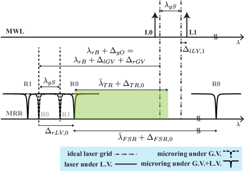
In this section, we develop a wavelength-domain model for multi-wavelength lasers and microring rows. We denote pre/post-fabrication laser and microring wavelengths , and , , respectively. Variation parameters have confidence interval bounds denoted by , and their sampled values are represented by . The model is summarized in Fig. 2 and Table I.
The pre-fabrication laser model is derived from the existing commercial standards such as CW-WDM MSA [29]. Each laser wavelength can be written as
| (1) |
where denotes the center wavelength and is the index of the wavelength in the wavelength-domain ordering, ranging from to . Default parameters for , and are chosen as \qty1300\nano, 8 and \qty1.12\nano (\qty200\giga in O-band), respectively. Note that a specific choice of is not relevant to our focus. For wavelength arbitration, only the relative distances between wavelengths matter.
The pre-fabrication microring model is derived in an analogous manner. The difference is that microring wavelengths are pre-biased to the blue-side by resonance wavelength bias () to account for the strict red-shifting of microring thermal tuning [22, 2]. Additionally, we define to correspond to the spatial location of a microring; the th microring is the th closest microring in a row from the light input side (See Fig. 1(a)). is defined as a map between the spatial ordering and spectral ordering of the microring row at pre-fabrication333 is similarly similarly, but refers to the target post-arbitration ordering.. We note that does not need to follow the natural ordering; it can be chosen by the designer for purposes such as for crosstalk optimization [28]. The pre-fabrication microring wavelength is written as
| (2) |
Default parameter for is chosen as \qty4.48\nano to maximize the distance from the laser center wavelength and keep the microring resonances lower than the laser wavelengths [22].
A major difference with the post-fabrication model is the addition of global and local variations due to the high sensitivity of photonic devices to fabrication and environmental variations. Various variability models have been proposed for integrated photonics [30, 31, 32, 33, 34, 35]; however, for our focus, we adopt a simplified approach for our purpose: considering only global (all-channel) and local (per-channel) variations. They are denoted in our model as and for the laser and and for the microring, respectively. To simplify further, we lump the global variations ( and ) into the “grid offset variation” between the microring row and laser wavelengths, which we call the grid offset (). This is possible because only the relative distances matter in our discussion. Since those global variations are uncorrelated, we simply sum the two to derive the grid offset444Strictly speaking, typically denotes the statistical variance where uncorrelated sums are sum-of-squares. In this paper, we use a linear sum for simplicity.. Without loss of generality, we add the grid offset to the post-fabrication laser wavelength model.
The post-fabrication multi-wavelength laser model can be written as
| (3) |
where denotes the sampled grid offset and denotes the sampled laser local variation at the th laser wavelength. The default parameter for corresponds to the channel bandwidth in the CW-WDM MSA specification [29], which is 25% of the grid spacing (). This value is a conservative estimate since reported multi-wavelength laser sources have consistently achieved better local variation [36, 37, 38, 39]. can be understood as the sum of center wavelength offset and variation range in CW-WDM MSA, which corresponds to the fabrication and environmental variations and specified as \qty5\nano and \qty4\nano, respectively. Thus, we assume the total laser global variation () to be \qty9\nano. For , we choose a default value of \qty6\nano, which we explain in the next paragraph.
The post-fabrication microring row model is expressed as
| (4) |
where denotes the sampled resonance local variation at the th microring wavelength. It is useful to note that most of the microring variations arise from global resonance variation (wafer-to-wafer and inter-die [32]), which can be partially mitigated by barrel-shifting the microring spectral ordering. Global process variations can be as large as \qty12\nano [33] due to substrate thickness and etch depth variations during fabrication [33, 40, 35, 41]. However, we assume the total microring global variation () to be \qty6\nano, as process variation can also be mitigated by die binning [33]. External thermal aggressions can also impact global resonance variation; however, it is difficult to characterize this effect without a well-defined deployment environment, such as that described by Lee et al. [8], which we do not include in our analysis. Microring local variation (), often referred to as channel-to-channel spacing variation, is the result of intra-die process variation and systematic error. However, it is challenging to extract a simple model for local variation due to the following factors: Systematic error refers to any deviation from ideal channel spacing that arises during the implementation of resonance stepping, which is typically achieved by incrementing ring radii. This process is particularly prone to design-time errors. In addition, intra-die process variation has a strong dependency on the physical distance between the microrings [42, 31, 33, 35], making it difficult to generalize across designs. Rather than pursuing a highly detailed local variation model, we employ a zeroth-order approach, selecting a single-valued as an upper bound to capture worst-case variations. The default value is set to \qty2.24\nano which is . However, for most cases, we sweep this value from \qty0.28\nano () to \qty8.96\nano () to observe the system’s behavior under different microring variations.
The tuning range of the th microring can be represented as a union of intervals with a width corresponding to the tuning range and spaced by the free spectral range (FSR):
| (5) |
where denotes the total tuning range, denotes the FSR of the th microring, denotes the tuning range of the th microring, and . Additionally, and , where is the sampled FSR variation at the th microring and is the sampled tuning range variation at the th microring. In a typical DWDM architecture, microring FSR is maximally filled with wavelength grids, or , which is the value we choose (\qty8.96\nano or \qty1.6\tera). The variation in the FSR () is known to be relatively well-controlled, typically around 1% [23, 41, 43]. While we assign a default parameter of \qty2.24\nano for tuning range (), we typically sweep the value from \qty1.12\nano () to \qty10.08\nano () [44] and observe the trend. For tuning range variation (), we assume a 10% variation based on the typical process, voltage and temperature variations of the tuner circuit.
The final simplification concerns the variation distributions, which we model as uniform distributions bounded by their confidence intervals (). This represents a significant departure from the commonly assumed Gaussian distribution. However, this approach can be seen as a conservative simplification of a trimmed Gaussian distribution, where the extremities are sampled more frequently. This simplification enables a more sample-efficient exploration of the statistical bounds necessary for achieving perfect arbitration success. Additionally, it can be easily adjusted for specific use cases, such as yield analysis or global sensitivity analysis.
III Evaluation Methodology
In this section, we introduce the evaluation methodology for arbitration robustness. Previously, tuning strategies have been evaluated based on their resulting tuning power, which facilitates comparisons of algorithm efficiency [22, 24, 25, 26]. However, tuning power assumes arbitration success, whereas evaluating robustness requires accounting for arbitration failures. Moreover, policy and algorithm represent distinct aspects of arbitration design—system specification and implementation—and their separation must be accounted for in an efficient, hierarchical analysis. This necessitates a more detailed approach to devising simulation experiments and assessing arbitration robustness.
III-A Policy Evaluation
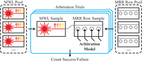
As the policy dictates wavelength arrangement post-arbitration, our simulation setup assumes wavelength-awareness during arbitration, which we refer to as the “ideal arbitration model.” This model arbitrates based on absolute wavelength values, effectively evaluating the arbiter’s specification independently from the wavelength-oblivious algorithm implementation. In particular, different policies correspond to varying levels of spectral ordering enforcement, leading to distinct sets of device parameters for arbitration success, which can be deduced from the wavelength-aware arbitration experiments.
We define Arbitration Failure Probability (AFP) as a metric to assess arbitration robustness under specific policy and varying system configurations. The system-under-test is generated by sampling multi-wavelength lasers and microring rows, with variations determined by their respective sources. Each system-under-test is subjected to an arbitration test using a specific policy and the ideal arbitration model. The number of arbitration failures is recorded, and AFP is calculated by dividing this number by the total number of trials. Essentially, AFP reflects the arbitration yield, where failure to arbitrate successfully is treated as transceiver failure, assuming accurate device models.
III-B Algorithm Evaluation
Since the algorithm operates in a wavelength-oblivious manner, the simulation setup uses the wavelength-oblivious arbitration model to reflect the algorithm’s operational constraints. While AFP can be used for algorithm evaluation, it may obscure the effectiveness of the algorithm due to the influence of the policy it implements. To isolate the effect of the algorithm implementation, we introduce a new metric: Conditional Arbitration Failure Probability (CAFP).
CAFP is defined as the conditional failure probability of the arbitration algorithm, given that the ideal arbitration under the same policy is successful. This metric quantifies how closely the algorithm approximates the behavior of the ideal arbitration model. CAFP is calculated by running tests using a specific algorithm and the wavelength-oblivious model, and recording failures that occur when the same system-under-test, under the corresponding policy, achieves arbitration success in the ideal model. The total failure rate, considering both the algorithm and the policy, can also be computed using conditional probability as follows:
| (6) | |||||
where, according to our notations, denotes the total failure probability, represents the CAFP, is the AFP of the corresponding policy, and is the probability of policy success. Note that , as the algorithm will always fail when the ideal arbitration fails.
IV Analysis of Arbitration Policy
In this section, we compare different arbitration policies and analyze their tradeoffs. We assume that three key parameters are considered during the arbitration design phase: arbitration policy, pre-fabrication microring spectral ordering and target post-arbitration microring spectral ordering . We select four main test cases for policy evaluation, namely LtA-N/A, LtA-P/A, LtC-N/N, and LtC-P/P, which are summarized in Table II. LtA and LtC stand for Lock-to-Any and Lock-to-Cyclic policies, as defined in Section II-A, according to their levels of spectral ordering enforcement. For pre-fabrication spectral ordering, we consider two specific instances: Natural and Permuted ordering. Natural refers to a straightforward ordering of for -DWDM. Permuted refers to , representing a sufficiently “shuffled” ordering instance. For post-arbitration spectral ordering, we assume the designer aims to match the pre-fabrication ordering555A case of , or “wavelength reconfiguration” [21] is beyond the scope of this paper., except in the case of the LtA policy, where post-arbitration spectral ordering is labeled “Any” indicating no specific enforcement. For each experiment, we conduct 10,000 trials, using 100 multi-wavelength lasers and 100 microring row samples. Unless otherwise noted, the default model parameters listed in Table I are used throughout the experiments.
| Configuration | LtA-N/A | LtA-P/A | LtC-N/N | LtC-P/P |
|---|---|---|---|---|
| Policy | Lock-to-Any | Lock-to-Cyclic | ||
| Natural3 | Permuted3 | Natural | Permuted | |
| Any3 | Any | Natural | Permuted | |
| 1 Pre-fabrication microring spectral ordering (see Table I) | ||||
| 2 Post-arbitration microring spectral ordering (see Table I) | ||||
| 3 Labels explained in the text above | ||||
IV-A General Trend
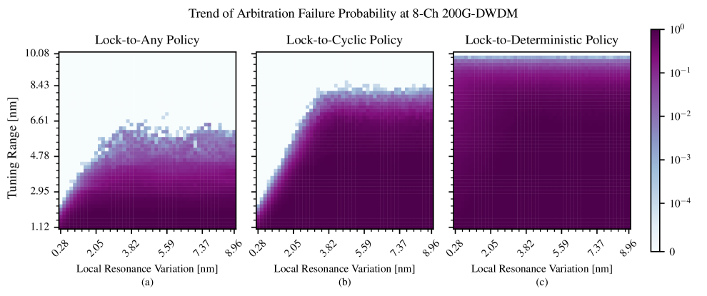
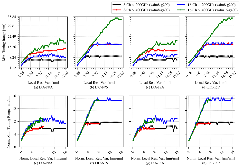
Fig. 4 illustrates the AFP across local resonance variation () and microring tuning range () values for different arbitration policies. In the plot, darker colors indicate higher AFP, with dark purple () representing complete arbitration failures for all trials, while brighter colors, particularly white (), indicate near or complete success. The plot exhibits a shmoo pattern: lower tuning ranges and higher resonance variations are more likely to result in arbitration failures, whereas higher tuning ranges and lower variations increase the likelihood of arbitration success. For each microring resonance variation value, we identify the minimum tuning range that achieves complete arbitration success, which we call the minimum tuning range. We use this minimum tuning range as a proxy to compare different policies and system configurations below.
The LtA policy has the lowest tuning range requirement, followed by the LtC and the LtD policy, reflecting how relaxed spectral ordering reduces the microring tuning range requirement. Fig. 5 shows the tuning range trends for different DWDM configurations, including wdm8/16, which refers to systems with 8 or 16 channels (), and g200/400, indicating channel spacings of \qty200\giga or \qty400\giga (). Both LtA and LtC policies exhibit a similar behavior, with their minimum tuning ranges saturating beyond a certain resonance variation. For LtA, saturation occurs around for wdm8 and for wdm16, as the microring resonance can be located anywhere within the FSR once the variation range, spanning to (totaling or the microring FSR), covers the entire FSR. LtC saturates earlier than LtA, likely because its minimum tuning range exceeds the microring FSR before the knee point of LtA’s tuning range requirement. Beyond the microring FSR, LtC arbitration success is expected to be guaranteed due to the resonance periodicity.
Before reaching saturation, both LtA and LtC exhibit a near-linear ramp in minimum tuning range, as shown in Fig. 5(e-h). The slope of the ramp is approximately 2, which we explain as follows: denotes the minimum tuning range at and denotes the minimum tuning range when . denotes the sampled local resonance variation for the th microring, and assume that microrings R0 through R() exhibit while R() exhibits . Due to the flexible target spectral ordering that allows cyclic-equivalent arrangements, LtA and LtC can achieve the minimum tuning distance of when all microrings exhibit a local resonance variation of . However, when only R() exhibits , an additional tuning distance is required, leading to a minimum tuning range of . LtA policy shows a slower ramp beyond , likely because it can find a matching pair that does not require additional tuning distance, especially at higher resonance variations.
Across DWDM configurations, wdm16-400g requires the most tuning range, followed by wdm8-400g, wdm16-200g, and wdm8-200g for LtA. LtC follows a similar trend, except that it has the same tuning range requirement for wdm8-400g and wdm16-200g, and it shows a larger gap between wdm16 and wdm8 configurations compared to LtA. This suggests that, for 16-channel cases (and likely 32-channel cases and beyond), LtA exhibits more favorable scaling than LtC in terms of tuning range requirements. However, when local variations are kept within , LtC becomes a competitive candidate due to its more deterministic spectral ordering. Denser channel spacing can also reduce the tuning range requirement, but this must be balanced against inter-microring crosstalk and multi-wavelength laser costs.
Lastly, the minimum tuning range for LtA-N/A shows no significant difference from LtA-P/A, nor for LtC-N/N compared to LtC-P/P. This can be explained using a simple 2-WDM model: If two arbitration trials with microrings R0 and R1 are identical but one has a pre-fabrication spectral ordering and the other has , then the required tuning for R0 and R1 will effectively swap, but the minimum of two would be the same for both trials. Thus, for ideal wavelength-aware arbitration, the difference in pre-fabrication ordering (with post-arbitration ordering for LtC) does not affect the minimum tuning range for either LtA or LtC. This suggests that pre-fabrication and post-arbitration spectral ordering can be flexibly assigned, and their selection is not necessarily constrained by tuning range requirements.
Next, we turn to case-studies to explore the impact of individual design parameter in greater detail.
IV-B Case of Lock-to-Deterministic Policy
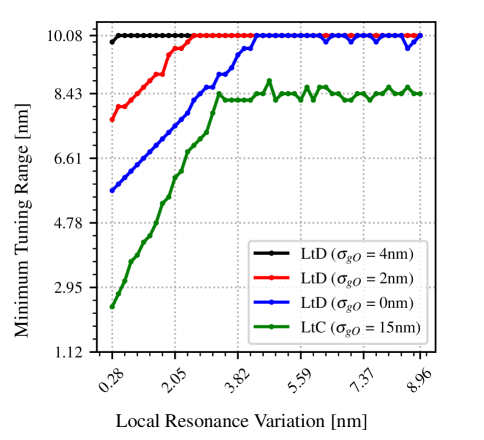
The LtD policy requires a significantly larger microring tuning range than both the LtC and LtA policies to achieve perfect arbitration success, as demonstrated in previous work [22] and Fig. 4. Since LtD requires microrings to be tuned by at least the grid offset to match corresponding laser wavelengths, we analyze the dependency of the minimum tuning range on the grid offset, as illustrated in Fig. 6. For small grid offsets ( \qty4\nano), LtD exhibits a linear increase in the minimum tuning range until it saturates, whereas larger grid offsets ( \qty4\nano) result in tuning ranges exceeding the FSR for any resonance local variation (). The linear slope is approximately 1, because LtD requires microrings to be tuned exactly to the laser wavelength order, and when microrings exhibit a blue-shift (), the required tuning distance increases by . As the grid offset adds directly to the required tuning distance, LtD quickly drives the minimum required tuning range beyond the FSR, which limits its practicality. To keep the grid offset below \qty4\nano and mitigate the large tuning range demands of LtD, both laser global variation () and microring global variation () must be controlled and minimized. However, microring global variation alone can easily surpass \qty4\nano, primarily due to substrate thickness variations (see Section II-C), which may create difficulties in adopting the LtD policy. Additionally, while the result is somewhat sensitive to the blue-shift fabrication bias ( in Table I) in microrings relative to laser wavelengths, this does not significantly alter our observation.
IV-C Impact of Laser and Microring Variabilities
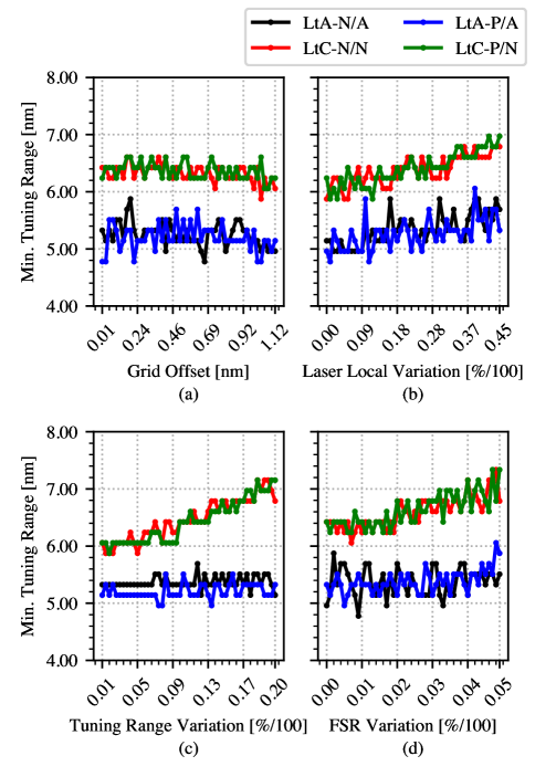
Next, we examine the impact of device variation parameters on arbitration robustness. Fig. 7 shows the local sensitivity analysis of laser and microring variations on the minimum tuning range. Fig. 7(a) sweeps grid offset () from \qty0\nano to \qty1.12\nano (the grid spacing), since for LtA and LtC arbiters, a grid offset larger than the grid spacing does not change the required tuning distance. This is because barrel-shifting the target spectral ordering effectively re-centers the microring row by multiples of . This adjustment cancels out that amount from the required tuning distance and compensates for grid offsets larger than \qty1.12\nano. Fig. 7(b) sweeps laser local variation () from 1% to 45%, which nearly doubles the range of our default value, 25%. Fig. 7(c) sweeps microring tuning range variation () from 0% to 20%, twice the nominal circuit variation range 10%. Fig. 7(d) sweeps microring FSR variation () from 0% to 5%, with our nominal value chosen as 1%.
Overall, the analysis shows that the primary factors determining the required microring tuning range are microring local resonance variation and arbitration policy, while other laser and microring variations, such as tuning range variation and FSR variation, play secondary or tertiary roles. Moreover, the trend remains consistent between pre-fabrication and post-arbitration spectral orderings, as discussed in Section IV-A. In detail, both LtA and LtC show sensitivity to laser local variation, while LtC is additionally sensitive to microring tuning range variation and FSR variation. Denoting the minimum tuning range as , we deduce that for both LtC and LtA. This can be explained by the following example: Suppose a set of laser wavelengths has 25% local wavelength variations i.e., \qty0.28\nano. In one possible scenario, is shifted by \qty0.28\nano and is shifted by \qty0.28\nano. A microring assigned to must shift by an additional \qty0.56\nano, which roughly matches our observation. While the sensitivities to and in LtC arbitration can be explained similarly, it is interesting to note that in other cases, the impact of these variations is significantly reduced. This is likely due to the looser enforcement of spectral ordering in LtA, which allows the system to “absorb” or tolerate larger variations without requiring substantial adjustments in the tuning range.
IV-D FSR Design Guideline
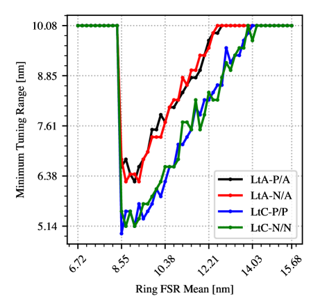
Lastly, we examine the design space of microring FSR (), as shown in Fig. 8. While the nominal design point is \qty8.96\nano, which is , is swept from \qty6.72\nano () to \qty15.68\nano () to investigate both under-design and over-design cases. For both LtA and LtC policies, we observe a tolerance range of approximately \qty0.5\nano around the nominal FSR, within which the increase in the minimum tuning range remains within \qty0.5\nano. Exceeding this tolerance range in the under-designed case causes a sharp increase in the required tuning range due to resonance aliasing, where may cause a single microring to align with multiple laser wavelengths, particularly under a 25% local laser variation666James et al. [43] proposed a multi-FSR scheme that allows by configuring the FSR and channel spacing to be coprime and assuming the use of a low-variation comb source, which is beyond the scope of our analysis.. Over-designing the FSR results in a more gradual increase in AFP. This occurs because as the FSR widens, the distance between the last microring grid and the first microring grid of the next FSR increases, which in turn increases the required tuning distances for the LtA and LtC policies. Therefore, to minimize AFP, it is preferable to design the FSR close to , with small deviations being acceptable.
V Wavelength Arbitration Algorithm
In this section, we explain an efficient and robust wavelength arbitration algorithm. We focus on the LtC policy implementation, while extensions to other policies are discussed in Section V-E. Our work extends the autonomous algorithm explained in Hattink et al. [17] by generalizing concepts such as target spectral ordering, conflict resolution, and maximum matching.
V-A Overview
The algorithm consists of two phases: record and matching, as illustrated in Fig. 9(a). The record phase tabulates the wavelength-domain relationship between the microring wavelength search outcomes of microring pairs. It is followed by the matching phase, where each microring is assigned to different laser wavelengths according to the identified relationships and the specified microring spectral ordering. For convenience, we refer to the relationship between microring wavelength search outcomes as the microring relation, and the process of identifying this relationship as the relation search. Fig. 9(b) summarizes the structure of the scheme.
During the record phase, (4 in Fig. 9(b)) relation searches are conducted to discover the microring relations between consecutive microring pairs. These pairs are derived from the target spectral ordering . In Fig. 9(b), given , the target pairs are , , , and . If , the pairs are , , and . We note that relation searches are not run across all microring pairs to construct a comprehensive “relation map” of wavelength search outcomes. Instead, we run relation searches on microring pairs. This is because the wavelength allocation for the LtC policy is semi-deterministic; if consecutive microring pairs from are allocated to neighboring wavelengths, then the wavelengths are assigned as desired. For example, it is sufficient for R to be assigned to the next laser wavelength of that assigned to R when . This property allows us to simplify the global arbitration problem into a set of arbitrations between consecutive pairs while guaranteeing robust operation.
Leveraging this simplification, the matching phase performs a non-iterative microring-to-laser matching by building the global lock allocation table. The table is constructed by rearranging the microring search tables based on the relations between consecutive pairs established during the record phase. From this table, the final wavelength allocation is derived in a single pass, with each microring assigned its lock target from its respective search table. The full procedure is detailed in Section V-C.
Before we delve into each phase, we define the nomenclature that are used in the rest of the sections. The search table in Fig. 9(b) is the recorded tuner codes of the microring corresponding to peak intra-cavity optical power during wavelength search. We denote the search table of the th microring as ST. A microring relation connects the two search tables and is mathematically formulated as the relation index, representing the offset between the search table entry locations according to the wavelength correspondence. We denote the relation index between the th and the th microring as . We use the relation index to align the search tables by wavelength alignment, forming the lock allocation table for efficient arbitration. Fig. 9(c) depicts the arbitration success, while Fig. 9(d-f) depicts different failures cases: two microrings are assigned to the same wavelengths (Dupl-Lock in Fig. 9(d)); one or more microrings are not assigned to any wavelength (Zero-Lock in Fig. 9(e)); lane-order mismatch or microring spectral ordering requirement is not met (Lane-Order Error in Fig. 9(f)).
V-B Record Phase
A core operation of the record phase is the relation search, which is illustrated in Fig. 10. The procedure is described in Hattink et al. [17] which utilizes the natural precedence order in light receive between the microrings. In a typical microring-based DWDM architecture, when light propagates to the downstream microrings, a microring physically closer to the light input has priority in light receive over farther rings. In other words, physical prior maps to the precedence order in capturing the wavelengths. Using this property, the relation search assigns the aggressor and victim roles within the microring pair according to their physical order. Both microrings first undergo the wavelength search, recording their initial search tables. Then, the aggressor microring “injects” aggression into the victim microring by wavelength lock to a specific target from ST. If the target is set appropriately, the victim microring will find one of the entries in its search table masked, indicating that the target chosen from ST and the masked entry in ST correspond to the same wavelength. Furthermore, other relations between the search table pairs can be inferred. For example, in Fig. 10, if 3rd entry of ST and 2nd entry of ST correspond to the same wavelength, then 2nd entry of ST and 1st entry of ST also correspond to the same wavelength, given that the microring tuning is monotonic in wavelength-domain. We call these identified and inferred relations a relation map between the microrings, and define Relation Index as the difference in indices between the masked entry and the aggressor target entry from each search table. Note that the aggressor target wavelength should be within the victim microring tuning range, which is not trivial in a wavelength-oblivious scenario.
To achieve a proper aggressor injection, it is most straightforward to loop through the aggressor search table entries and repeat the relation search. However, for efficient arbitration, it is desirable to find a more systematic way that determines the aggressor lock target, as shown in Fig. 11(a). Without loss of generality, we assume . From our notation in Section II-C, R physically precedes R, making R the aggressor and R the victim. In Fig. 11(a), which depicts the case of , we notice that setting the aggressor lock target to the last entry (Lock-to-Last) achieves the aggressor injection when the microring relation exists. When , as shown in Fig. 11(b), setting the aggressor target to the first entry (Lock-to-First) achieves the aggressor injection. While the pre-fabrication spectral ordering sets the initial microring ordering, process variations can cause the post-fabrication spectral orderings to be “flipped”. Thus, we run both aggressions and combine the results for .
However, in case of large microring variations, neither aggressor Lock-to-First nor Lock-to-Last achieves the aggressor injection. Fig. 11(c) illustrates the case of large tuning range variation, and Fig. 11(d) shows the case of large FSR variation, where both the first and last targets are outside the victim microring’s tuning range. In these cases, we re-run the relation search with the aggressor Lock-to-Second and find the relation. This simple scheme, which we call Variation-Tolerant Relation Search (VT-RS) trades off robustness with additional overhead. We further study this in Section V-D.
V-C Matching Phase
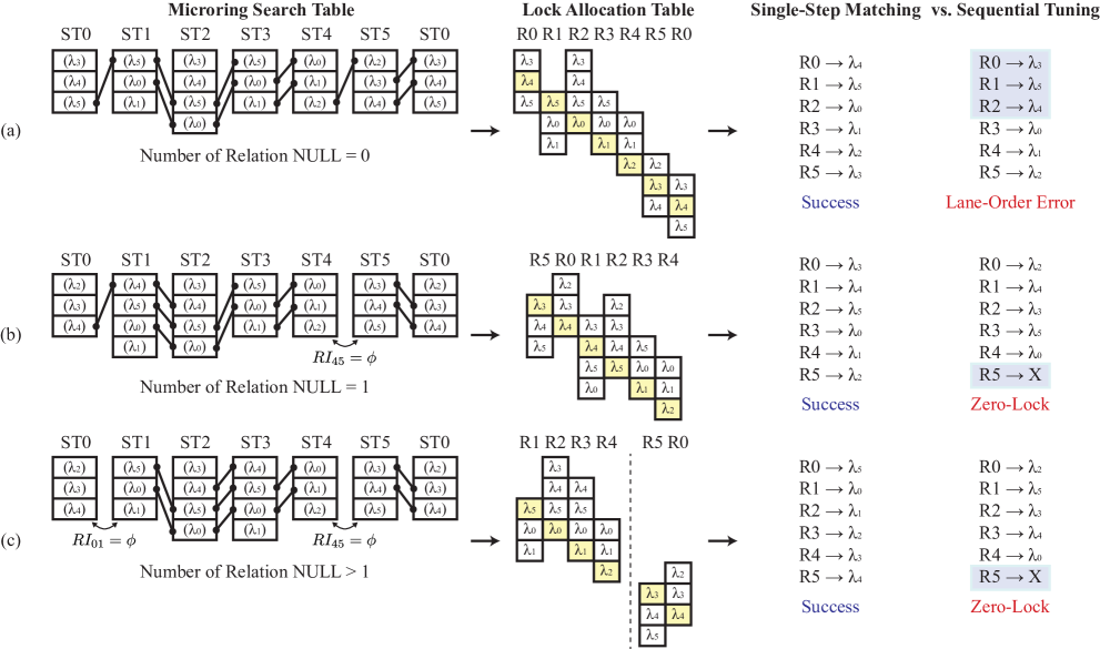
We describe our non-iterative matching algorithm for the LtC arbitration, which we call the Single-Step Matching (SSM) algorithm. A key data structure is the lock allocation table, which provides a global view of the wavelength lock candidates for microrings in the wavelength domain. As illustrated in Fig. 12(a), the table is constructed by organizing the search tables into a two-dimensional structure, where the horizontal axis represents different microrings and the vertical axis represents search table entries, or lock candidates. The relation index is used to vertically offset the search tables so that entries at the same vertical position correspond to the same wavelength, while the tables are arranged horizontally based on the target spectral ordering (). The algorithm then assigns lock targets to each microring through an ordered assignment, achieving a non-iterative matching that follows the specified target ordering. While this approach works smoothly when all relation searches return a valid relation index, special attention is needed when any search fails to find a relation index, which we denote as . In such cases, we assume that the microring resonance wavelengths are “grouped” and form the sub-allocation tables according to the occurrences of .
Fig. 12(b) illustrates the formation of sub-allocation tables and lock target assignment when certain relation searches fail to find a relation index. In Fig. 12(b), with , relation searches are conducted between the pairs (R0, R1), (R1, R2), (R2, R3) and (R3, R0). The relation searches between (R0, R1) and (R2, R3) returns empty indices ( and ). Based on these occurrences, we interpret (R1, R2) and (R3, R0) as clustered and form sub-allocation tables accordingly. We then assign the lock targets of R1 and R0—the aggressor/victim microrings in the relation search that yields —to the first and last entries of their respective microring search tables. This strategy can replicate the outcome of the ideal wavelength-aware LtC arbitration, and we prove this by contradiction: If the wavelength-aware LtC allocation is feasible but this strategy fails, it implies the existence of an alternative valid assignment. Without loss of generality, assume the valid assignment for R1 is an entry other than the first entry in its search table, while R0 is assigned the last entry of ST0. R0 and R1 should be assigned neighboring wavelengths (); However, the first entry of ST1 would fall between those wavelengths, contradicting the assumption of a valid assignment.
Fig. 13 summarizes the proposed Single-Step Matching algorithm. The algorithm is applied on a case-by-case basis, depending on the number of occurrences. If does not occur, a single lock allocation table is created, and the assignment problem becomes a diagonal matching process. When occurs more than once, sub-allocation tables are formed, separated by the microring pairs that corresponds to . The first microrings in each sub-table are assigned the first entries from their search tables, while the last microrings are assigned the last entries. In case where occurs once, a single allocation table is formed, starting and ending with the microring pair corresponding to . Fig. 13 also compares the results of the Single-Step Matching algorithm with the sequential tuning scheme, where the first available wavelength is assigned to each microring sequentially. Sequential tuning fails at the last microring for both Fig. 13(b) and (c). This failure occurs because the sequential assignment can cause earlier microrings to “steal” all available wavelengths, leaving none for the later microrings—a problem that our proposed algorithm avoids through its tabulated approach.
V-D Evaluation of Proposed Schemes
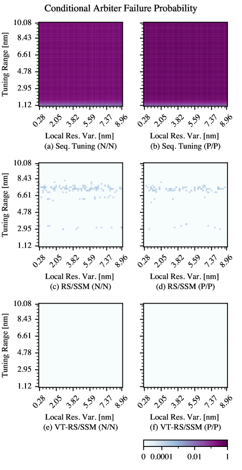
We evaluate the proposed algorithms using Conditional Arbitration Failure Probability (CAFP), as described in Section III. Measured CAFP indicates how effectively the algorithm implements the LtC policy by evaluating its failure rate when the ideal LtC arbitration succeeds. The algorithms are denoted as RS/SSM and VT-RS/SSM. RS/SSM represents the Relation Search for the record phase and Single-Step Matching for the matching phase, while VT-RS/SSM refers to the Variation-Tolerant Relation Search for the record phase and Single-Step Matching for the matching phase. The baseline used is the sequential tuning scheme, which sequentially tunes the microrings and assigns them to the nearest wavelengths (Lock-to-Nearest) [6, 22, 23, 45]. We focus on two representative target microring spectral orderings (): Natural (N) and Permuted (P), as defined in Section IV. The baseline sequential tuning is extended to arbitrary spectral orderings as follows: For Natural ordering (), R0 is tuned first, followed by R1, and so on. For Permuted ordering (), R0 is tuned first, followed by R2 (the microring corresponding to the second spectral order), and so on. As in Section IV, we assume the pre-fabrication spectral ordering () matches the post-arbitration target ordering (). The default model parameters in Table I are used for the experiments, with 10,000 arbitration tests conducted using 100 multi-wavelength laser and microring row samples.
Fig. 14 shows the CAFP across different local resonance variations () and microring tuning ranges (), with the choice of sweep ranges explained in Section II-C. We observe that the proposed schemes consistently outperform the baseline in all cases, with VT-RS/SSM closely approximating the ideal LtC arbitration. The errors observed in RS/SSM at tuning ranges around \qty8\nano likely stem from a tuning range variation of \qty0.8\nano (10% of \qty8\nano), which is significant enough to introduce errors during the relation search, as discussed in Section V-B. These errors can be systematically mitigated by reducing the tuning range below \qty8\nano or using VT-RS instead. Furthermore, as demonstrated in Fig. 14(b), (d), and (f), the scheme is applicable to any target spectral ordering, assuming .
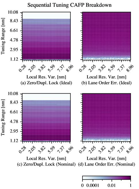
The plotted CAFP metric includes lane-order mismatch errors (Fig. 9(f)) due to the assumed LtC arbitration, whereas the sequential tuning scheme may not necessarily target a specific spectral ordering. For fair comparison, in Fig. 15, we break down CAFP of sequential tuning into two categories: zero/duplicate lock errors (Fig. 9(d) and (e)) and lane-order mismatch errors (Fig. 9(f)). When the microring tuning range is larger than approximately the FSR (\qty8.96\nano), lane-order mismatch errors dominate the CAFP. On the other hand, when the tuning range is smaller than the FSR, the sequential tuning scheme shows significant zero/duplicate lock errors, even with ideal laser variations and microring FSR/tuning range variations. This is likely due to microring local resonance variations larger than \qty0.28\nano, which is 1/4 of the channel spacing, still contributing significantly to lock errors in the sequential tuning scheme. Empirical observations suggest that many sequential tuning failures are due to missing the last few microrings. Future work will explore this issue further.
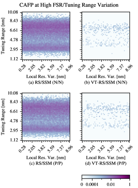
Finally, Fig. 16 compares the CAFP of the proposed RS/SSM and VT-RS/SSM under high microring FSR and tuning range variations. The plot suggests an interesting trend, with bands of CAFP forming around tuning ranges of \qty3\nano and \qty8\nano. These bands can be linked to the relation search failure cases illustrated in Fig. 11(c) and (d). Specifically, we associate the band around \qty3\nano with high FSR variation, while the band around \qty8\nano would correspond to both high tuning range and FSR variations. Fig. 16(c) and (d) show similar bands, implying a consistent trend across different target spectral orderings.
While an FSR variation of 5% and a tuning range variation of 20% may be unrealistically high, Fig. 16(b) and (d) demonstrate that VT-RS/SSM still performs well under these harsh conditions. However, this performance comes with additional overhead, including extra steps such as aggressor Lock-to-Second and victim wavelength searches in VT-RS/SSM. Therefore, selecting an algorithm should be done holistically, taking into account factors such as microring variations, failure tolerance levels (yield impact), and initialization costs.
V-E Discussion
The design and evaluation of the wavelength arbitration algorithms has been discussed. These algorithms complement previous studies on physical implementations, such as wavelength search [11] and lock [14, 15], innovative architectures like thermal crosstalk-aware control [46], and efficient DWDM microring wavelength lock architectures [18, 19, 20]. The schemes are applicable to both transmitters (TX) and receivers (RX) as the arbitration pertains to wavelength allocation step. For instance, a DWDM TX would then require a maximum Optical Modulation Amplitude wavelength lock similar to those in Sun et al. [11] and Grimaldi et al. [15], after allocation.
We outline several potential directions for future work. First, this study does not fully explore the implementations of the LtD and LtA policies. For the LtD policy, a pilot signal is likely necessary since the relation search only reveals relative wavelength positions. Without it, distinguishing between wavelengths would be impractical. For the LtA policy, constructing a full relation map for allocation to any spectral ordering would require relation searches between all microring pairs. Additionally, typical maximum matching algorithms, which involve backtracking, would significantly diverge from the proposed single-step method. Second, scaling the microring FSR beyond 32/64-channel configurations may not be feasible if the FSR is set to . In such cases, the analysis and the algorithms should be adapted to the multi-FSR scheme proposed by James et al. [43]. Lastly, future research could extend the current framework to account for transceiver-level interactions [24, 25, 26], which would provide a more comprehensive evaluation of system performance and refine the algorithms to ensure robustness across both TX and RX.
VI Conclusion
In this paper, we addressed the critical challenge of aligning microring resonances with laser wavelengths in microring-based DWDM transceivers, a process we termed wavelength arbitration. We introduced an ideal arbitration model that decouples the analysis of policy and algorithm, providing a framework for evaluating the efficacy of different arbitration strategies. Our hierarchical formulation allows for the independent assessment of arbitration policies from algorithm implementations, simplifying the analysis of both layers.
To effectively define the DWDM interface, we introduced three arbitration policies—LtA, LtC, and LtD—categorized by their spectral ordering enforcement levels and evaluated their tradeoffs in the design space. Furthermore, we developed a wavelength-oblivious algorithm for LtC policy implementation, including the RS/SSM and VT-RS/SSM. Through extensive simulations, we demonstrated that our schemes closely approximate the ideal model, significantly outperforming the traditional sequential tuning approach.
Our findings underscore the importance of adopting a holistic approach to wavelength arbitration, where policy-driven arbitration, alongside algorithmic implementations, enables scalable and reliable wavelength allocation. By evaluating arbitration strategies through AFP and CAFP metrics, we provide a comprehensive view of how these strategies perform across varying device-level conditions and system configurations. This work establishes a foundation for advanced arbitration techniques, demonstrating the need to integrate both high-level policy design and practical, wavelength-oblivious algorithm implementation. Moving forward, further research into variations such as LtA policy implementations will be crucial for enhancing the scalability and robustness of microring-based DWDM transceivers.
Acknowledgments
This work was supported in part by task 3132.015 of the Center for Ubiquitious Connectivity (CUbiC), sponsored by Semiconductor Research Corporation (SRC) and Defence Advanced Research Projects Agency (DARPA) under the JUMP 2.0 program. Sunjin Choi would like to acknowledge the support from Korea Foundation for Advanced Studies (KFAS) and Qualcomm Innovation Fellowship (QIF). The authors would like to thank Shenggao Li from TSMC and Pavan Bhargava from Ayar Labs for their valuable discussions and feedback. The authors would like to give special thanks to Yue Dai for her valuable assistance in writing the manuscript. The authors also acknowledge the students, staff, faculty and sponsors of the Berkeley Wireless Research Center.
References
- [1] M. Wade, E. Anderson, S. Ardalan, P. Bhargava, S. Buchbinder, M. L. Davenport, J. Fini, H. Lu, C. Li, R. Meade et al., “Teraphy: A chiplet technology for low-power, high-bandwidth in-package optical i/o,” IEEE Micro, vol. 40, no. 2, pp. 63–71, 2020.
- [2] D. Liang, S. Srinivasan, G. Kurczveil, B. Tossoun, S. Cheung, Y. Yuan, A. Descos, Y. Hu, Z. Huang, P. Sun et al., “An energy-efficient and bandwidth-scalable dwdm heterogeneous silicon photonics integration platform,” IEEE Journal of Selected Topics in Quantum Electronics, vol. 28, no. 6: High Density Integr. Multipurpose Photon. Circ., pp. 1–19, 2022.
- [3] C. S. Levy, Z. Xuan, J. Sharma, D. Huang, R. Kumar, C. Ma, G.-L. Su, S. Liu, J. Kim, X. Wu et al., “8- 50 gbps/ heterogeneously integrated si-ph dwdm transmitter,” IEEE Journal of Solid-State Circuits, 2024.
- [4] Z. Xuan, G. Balamurugan, D. Huang, R. Kumar, J. Sharma, C. Levy, J. Kim, C. Ma, G.-L. Su, S. Liu et al., “A 256 gbps heterogeneously integrated silicon photonic microring-based dwdm receiver suitable for in-package optical i/o,” in 2023 IEEE Symposium on VLSI Technology and Circuits (VLSI Technology and Circuits). IEEE, 2023, pp. 1–2.
- [5] Y. Wang, S. Wang, R. Parsons, A. Novick, V. Gopal, K. Jang, A. Rizzo, C.-P. Chiu, K. Hosseini, T. T. Hoang et al., “Silicon photonics chip i/o for ultra high-bandwidth and energy-efficient die-to-die connectivity,” in 2024 IEEE Custom Integrated Circuits Conference (CICC). IEEE, 2024, pp. 1–8.
- [6] P.-H. Chang, A. Samanta, P. Yan, M. Fu, Y. Zhang, M. B. On, A. Kumar, H. Kang, I.-M. Yi, D. Annabattuni et al., “A 3d integrated energy-efficient transceiver realized by direct bond interconnect of co-designed 12 nm finfet and silicon photonic integrated circuits,” Journal of Lightwave Technology, vol. 41, no. 21, pp. 6741–6755, 2023.
- [7] C. Sun, C.-H. O. Chen, G. Kurian, L. Wei, J. Miller, A. Agarwal, L.-S. Peh, and V. Stojanovic, “Dsent-a tool connecting emerging photonics with electronics for opto-electronic networks-on-chip modeling,” in 2012 IEEE/ACM Sixth International Symposium on Networks-on-Chip. IEEE, 2012, pp. 201–210.
- [8] B. G. Lee, N. Nedovic, T. H. Greer, and C. T. Gray, “Beyond cpo: A motivation and approach for bringing optics onto the silicon interposer,” Journal of Lightwave Technology, vol. 41, no. 4, pp. 1152–1162, 2023.
- [9] N. Nedovic, “Methodology for device, circuit and architecture level co-design and optimization of dense wavelength division multiplexing links,” in CLEO 2023. Optica Publishing Group, 2023, p. AM1Q.2. [Online]. Available: https://opg.optica.org/abstract.cfm?URI=CLEO_AT-2023-AM1Q.2
- [10] J. C. Mak and J. K. Poon, “Multivariable tuning control of photonic integrated circuits,” Journal of Lightwave Technology, vol. 35, no. 9, pp. 1531–1541, 2017.
- [11] C. Sun, M. Wade, M. Georgas, S. Lin, L. Alloatti, B. Moss, R. Kumar, A. H. Atabaki, F. Pavanello, J. M. Shainline et al., “A 45 nm cmos-soi monolithic photonics platform with bit-statistics-based resonant microring thermal tuning,” IEEE Journal of Solid-State Circuits, vol. 51, no. 4, pp. 893–907, 2016.
- [12] C. Li, R. Bai, A. Shafik, E. Z. Tabasy, B. Wang, G. Tang, C. Ma, C.-H. Chen, Z. Peng, M. Fiorentino et al., “Silicon photonic transceiver circuits with microring resonator bias-based wavelength stabilization in 65 nm cmos,” IEEE journal of solid-state circuits, vol. 49, no. 6, pp. 1419–1436, 2014.
- [13] M. de Cea, A. H. Atabaki, and R. J. Ram, “Power handling of silicon microring modulators,” Opt. Express, vol. 27, no. 17, pp. 24 274–24 285, Aug 2019. [Online]. Available: https://opg.optica.org/oe/abstract.cfm?URI=oe-27-17-24274
- [14] K. Padmaraju, D. F. Logan, T. Shiraishi, J. J. Ackert, A. P. Knights, and K. Bergman, “Wavelength locking and thermally stabilizing microring resonators using dithering signals,” Journal of Lightwave Technology, vol. 32, no. 3, pp. 505–512, 2014.
- [15] V. Grimaldi, F. Zanetto, F. Toso, I. Roumpos, T. Chrysostomidis, A. Perino, M. Petrini, F. Morichetti, A. Melloni, N. Pleros, M. Moralis-Pegios, K. Vyrsokinos, G. Ferrari, and M. Sampietro, “Self-stabilized 50 gb/s silicon photonic microring modulator using a power-independent and calibration-free control loop,” Journal of Lightwave Technology, vol. 41, no. 1, pp. 218–225, 2023.
- [16] H. Li, G. Balamurugan, T. Kim, M. N. Sakib, R. Kumar, H. Rong, J. Jaussi, and B. Casper, “A 3-d-integrated silicon photonic microring-based 112-gb/s pam-4 transmitter with nonlinear equalization and thermal control,” IEEE Journal of Solid-State Circuits, vol. 56, no. 1, pp. 19–29, 2021.
- [17] M. Hattink, Z. Zhu, and K. Bergman, “Automated tuning and channel selection for cascaded micro-ring resonators,” in Metro and Data Center Optical Networks and Short-Reach Links III, vol. 11308. SPIE, 2020, pp. 160–168.
- [18] M. Hattink, L. Y. Dai, Z. Zhu, and K. Bergman, “Streamlined architecture for thermal control and stabilization of cascaded dwdm micro-ring filters bus,” in Optical Fiber Communication Conference. Optica Publishing Group, 2022, pp. W2A–2.
- [19] P. Dong, R. Gatdula, K. Kim, J. H. Sinsky, A. Melikyan, Y.-K. Chen, G. De Valicourt, and J. Lee, “Simultaneous wavelength locking of microring modulator array with a single monitoring signal,” Optics express, vol. 25, no. 14, pp. 16 040–16 046, 2017.
- [20] Z. Wang, D. Ming, Y. Wang, K. X. Wang, X. Xiao, X. Zhang, and M. Tan, “An electronic-photonic converged adaptive-tuning-step pipelined time-division-multiplexing control scheme for fast and scalable wavelength locking of micro-rings,” Journal of Lightwave Technology, vol. 40, no. 16, pp. 5622–5630, 2022.
- [21] H.-K. Kim, J.-H. Lee, M. Kim, Y. Jo, S. Lischke, C. Mai, L. Zimmermann, and W.-Y. Choi, “A 4- 28-gb/s/ silicon ring-resonator-based wdm receiver with a reconfigurable temperature controller,” Journal of Lightwave Technology, vol. 42, no. 7, pp. 2296–2302, 2024.
- [22] M. Georgas, J. Leu, B. Moss, C. Sun, and V. Stojanović, “Addressing link-level design tradeoffs for integrated photonic interconnects,” in 2011 IEEE Custom Integrated Circuits Conference (CICC). IEEE, 2011, pp. 1–8.
- [23] A. V. Krishnamoorthy, X. Zheng, G. Li, J. Yao, T. Pinguet, A. Mekis, H. Thacker, I. Shubin, Y. Luo, K. Raj, and J. E. Cunningham, “Exploiting cmos manufacturing to reduce tuning requirements for resonant optical devices,” IEEE Photonics Journal, vol. 3, no. 3, pp. 567–579, 2011.
- [24] Y. Wang, P. Sun, J. Hulme, M. A. Seyedi, M. Fiorentino, R. G. Beausoleil, and K.-T. Cheng, “Energy efficiency and yield optimization for optical interconnects via transceiver grouping,” Journal of Lightwave Technology, vol. 39, no. 6, pp. 1567–1578, 2021.
- [25] Y. Wang, M. A. Seyedi, R. Wu, J. Hulme, M. Fiorentino, R. G. Beausoleil, and K.-T. Cheng, “Energy-efficient channel alignment of dwdm silicon photonic transceivers,” in 2018 Design, Automation & Test in Europe Conference & Exhibition (DATE). IEEE, 2018, pp. 601–604.
- [26] R. Wu, M. A. Seyedi, Y. Wang, J. Hulme, M. Fiorentino, R. G. Beausoleil, and K.-T. Cheng, “Pairing of microring-based silicon photonic transceivers for tuning power optimization,” in 2018 23rd Asia and South Pacific Design Automation Conference (ASP-DAC). IEEE, 2018, pp. 135–140.
- [27] D. D. Sharma, “System on a package innovations with universal chiplet interconnect express (ucie) interconnect,” IEEE Micro, vol. 43, no. 2, pp. 76–85, 2023.
- [28] M. Bahadori, S. Rumley, H. Jayatilleka, K. Murray, N. A. Jaeger, L. Chrostowski, S. Shekhar, and K. Bergman, “Crosstalk penalty in microring-based silicon photonic interconnect systems,” Journal of Lightwave Technology, vol. 34, no. 17, pp. 4043–4052, 2016.
- [29] CW-WDM MSA, “CW-WDM MSA Technical Specifications Rev 1.0,” CW-WDM MSA, https://cw-wdm.org/, Technical Specifications, 2020, accessed: June 25, 2024.
- [30] D. S. Boning, S. I. El-Henawy, and Z. Zhang, “Variation-aware methods and models for silicon photonic design-for-manufacturability,” Journal of Lightwave Technology, vol. 40, no. 6, pp. 1776–1783, 2022.
- [31] Z. Lu, J. Jhoja, J. Klein, X. Wang, A. Liu, J. Flueckiger, J. Pond, and L. Chrostowski, “Performance prediction for silicon photonics integrated circuits with layout-dependent correlated manufacturing variability,” Optics express, vol. 25, no. 9, pp. 9712–9733, 2017.
- [32] Y. Wang, J. Hulme, P. Sun, M. Jain, M. A. Seyedi, M. Fiorentino, R. G. Beausoleil, and K.-T. Cheng, “Characterization and applications of spatial variation models for silicon microring-based optical transceivers,” in 2020 57th ACM/IEEE Design Automation Conference (DAC). IEEE, 2020, pp. 1–6.
- [33] P. Sun, J. Hulme, T. Van Vaerenbergh, J. Rhim, C. Baudot, F. Boeuf, N. Vulliet, A. Seyedi, M. Fiorentino, and R. G. Beausoleil, “Statistical behavioral models of silicon ring resonators at a commercial cmos foundry,” IEEE Journal of Selected Topics in Quantum Electronics, vol. 26, no. 2, pp. 1–10, 2020.
- [34] A. Waqas, D. Melati, and A. Melloni, “Sensitivity analysis and uncertainty mitigation of photonic integrated circuits,” Journal of Lightwave Technology, vol. 35, no. 17, pp. 3713–3721, 2017.
- [35] A. Mirza, F. Sunny, P. Walsh, K. Hassan, S. Pasricha, and M. Nikdast, “Silicon photonic microring resonators: A comprehensive design-space exploration and optimization under fabrication-process variations,” IEEE Transactions on Computer-Aided Design of Integrated Circuits and Systems, vol. 41, no. 10, pp. 3359–3372, 2022.
- [36] M. N. Sysak, R. Roucka, S. Liu, C. Li, F. Luna, J. Frey, M. Raval, C. Zhang, L.-F. Yang, M. Wade et al., “An uncooled cw-wdm msa compliant multi-wavelength laser source operating from 15-100oc for wdm cmos applications,” in Optical Interconnects XXII, vol. 12007. SPIE, 2022, pp. 141–143.
- [37] D. Huang, R. Kumar, X. Wu, K. N. Nguyen, G.-L. Su, M. Sakib, C. Ma, J. Heck, and H. Rong, “8-channel hybrid iii-v/silicon dfb laser array with highly uniform 200 ghz spacing and power,” in 2021 27th International Semiconductor Laser Conference (ISLC). IEEE, 2021, pp. 1–2.
- [38] X. Wang, R. Kumar, D. Huang, G.-L. Su, X. Wu, S. Liu, and H. Rong, “16-channel integrated multi-wavelength dfb lasers with 200 ghz channel spacing,” in Novel In-Plane Semiconductor Lasers XXIII, vol. 12905. SPIE, 2024, pp. 99–104.
- [39] J. Zhao, Z. Sun, Y. Zhang, Z. Wang, R. Xiao, Z. Yang, K. Tang, W. Sun, Z. Xu, Y. Ma et al., “Multi-wavelength dfb laser with high mode stability and uniform spacing for optical i/o technology,” Journal of Lightwave Technology, 2024.
- [40] S. K. Selvaraja, W. Bogaerts, P. Dumon, D. Van Thourhout, and R. Baets, “Subnanometer linewidth uniformity in silicon nanophotonic waveguide devices using cmos fabrication technology,” IEEE Journal of Selected Topics in Quantum Electronics, vol. 16, no. 1, pp. 316–324, 2010.
- [41] A. Mirza, R. E. Gloekler, J. Thompson, S. Pasricha, and M. Nikdsast, “Experimental analysis of adiabatic silicon photonic microring resonators under process variations,” IEEE Photonics Technology Letters, 2024.
- [42] L. Chrostowski, X. Wang, J. Flueckiger, Y. Wu, Y. Wang, and S. T. Fard, “Impact of fabrication non-uniformity on chip-scale silicon photonic integrated circuits,” in Optical Fiber Communication Conference. Optica Publishing Group, 2014, pp. Th2A–37.
- [43] A. James, A. Novick, A. Rizzo, R. Parsons, K. Jang, M. Hattink, and K. Bergman, “Scaling comb-driven resonator-based dwdm silicon photonic links to multi-tb/s in the multi-fsr regime,” Optica, vol. 10, no. 7, pp. 832–840, Jul 2023. [Online]. Available: https://opg.optica.org/optica/abstract.cfm?URI=optica-10-7-832
- [44] D. Coenen, H. Oprins, Y. Ban, F. Ferraro, M. Pantouvaki, J. Van Campenhout, and I. De Wolf, “Thermal modelling of silicon photonic ring modulator with substrate undercut,” Journal of Lightwave Technology, vol. 40, no. 13, pp. 4357–4363, 2022.
- [45] Y. Wang, A. Novick, R. Parsons, S. Wang, K. Jang, A. James, M. Hattink, V. Gopal, A. Rizzo, C.-P. Chiu et al., “Scalable architecture for sub-pj/b multi-tbps comb-driven dwdm silicon photonic transceiver,” in Next-Generation Optical Communication: Components, Sub-Systems, and Systems XII, vol. 12429. SPIE, 2023, pp. 271–288.
- [46] M. Milanizadeh, D. Aguiar, A. Melloni, and F. Morichetti, “Canceling thermal cross-talk effects in photonic integrated circuits,” Journal of Lightwave Technology, vol. 37, no. 4, pp. 1325–1332, 2019.
![[Uncaptioned image]](/html/2411.14810/assets/x17.png) |
Sunjin Choi (Student Member, IEEE) received the B.S. degree in electrical engineering and computer science from Seoul National University, Seoul, South Korea, in 2020. He is currently pursuing the Ph.D. degree in electrical engineering and computer sciences at the University of California, Berkeley, CA, USA. He has held an internship position with Ayar Labs and X, the moonshot factory, where he worked on integrated photonic system design. His research interests include design of electronic-photonic integrated systems for high-speed optical interconnects. |
![[Uncaptioned image]](/html/2411.14810/assets/x18.png) |
Vladimir Stojanović (Fellow, IEEE) received the Dipl.-Ing. degree from the University of Belgrade, Belgrade, Serbia, in 1998, and the Ph.D. degree in electrical engineering from Stanford University, Stanford, CA, USA, in 2005. He was with Rambus, Inc., Los Altos, CA, USA, from 2001 to 2004; and the Massachusetts Institute of Technology, Cambridge, MA, USA, as an Associate Professor, from 2005 to 2013. He is currently a Professor of electrical engineering and computer sciences with the University of California at Berkeley, Berkeley, CA, USA, where he is also a Faculty Co-Director of Berkeley Wireless Research Center (BWRC), Berkeley. His current research interests include the design, modeling, and optimization of integrated systems, from CMOS-based VLSI blocks and interfaces to system design with emerging devices, such as NEM relays and silicon photonics, design and implementation of energy-efficient electrical and optical networks, and digital communication techniques in high-speed interfaces and high-speed mixed-signal integrated circuit (IC) design. Dr. Stojanović was a recipient of the 2006 IBM Faculty Partnership Award, the 2009 NSF CAREER Award, the 2008 ICCAD William J. McCalla, the 2008 IEEE Transactions on Advanced Packaging Award, and the 2010 ISSCC Jack Raper Best Paper and 2020 ISSCC Best Forum Presenter Awards. He was a Distinguished Lecturer of IEEE Solid-State Circuits Society from 2012 to 2013. |