ScAlN-on-SiC Ku-Band Solidly-Mounted Bidimensional Mode Resonators
Abstract
This letter reports on Solidly-Mounted Bidimensional Mode Resonators (S2MRs) based on 30% Scandium-doped Aluminum Nitride (ScAlN) on Silicon Carbide (SiC), operating near 16 GHz. Experimental results demonstrate mechanical quality factors () as high as 380, electromechanical coupling coefficients () of 4.5%, an overall Figure of Merit () exceeding 17, and power handling greater than 20 dBm for devices closely matched to 50 . To the best of the authors’ knowledge, S2MRs exhibit the highest Key Performance Indicators (KPIs) among solidly mounted resonators in the Ku band, paving the way for the integration of nanoacoustic devices on fast substrates with high-power electronics, tailored for military and harsh-environment applications.
ScAlN, RF NEMS, Sezawa Mode
1 Introduction
Emerging communication paradigms are driving the demand for low Size, Weight, and Power (SWaP) Radio Frequency (RF) electronic components capable of performing signal processing, timing, and impedance matching in the Ku band and beyond [1][2]. Specifically, in the context of electromagnetic (EM) spectrum filtering, advanced 5G and proposed 6G commercial applications stand to benefit significantly from the development of compact, high-performance, and mass-manufacturable on-chip filters designed for handheld and wearable devices [3][4]. Similarly, Satellite Communications (SATCOM) and military applications, such as Active Electronically Scanned Arrays (AESA) [5], would greatly benefit from technologies that enable monolithic integration, high power handling, and reliable operation at elevated temperatures (up to hundreds of degrees Celsius) [6][7].
While traditional EM filters [8][9] and novel spintronic devices [10] remain bulky and challenging to scale, researchers have increasingly turned their attention to piezoelectric acoustic Micro- and Nanoelectromechanical Systems (M/NEMS) as a promising alternative for RF filtering at higher frequencies [11]. Acoustic MEMS devices, such as Surface Acoustic Wave (SAW) [12][13] and Film Bulk Acoustic Resonators (FBARs) [14][15], represent the state-of-the-art solutions in the field, offering high selectivity and low insertion loss () [16]. However, their performance beyond 5 GHz has been hindered by challenges such as declining quality factors () and the need to operate within the nanoacoustic domain, where sound propagation speeds are significantly lower than those of EM waves, increasing fabrication complexity [17].
Recent advances have demonstrated that acoustic NEMS devices can retain high factors even in the mmWave band [18], making them viable candidates for integrated nanoacoustic filters with performance metrics compatible with modern communication systems stringent requirements [19].
In this letter, nanoacoustic Solidly-Mounted Bidimensional Mode Resonators (S2MR) operating at approximately 16 GHz are presented. This class of devices leverages a slow-on-fast optimized Sezawa mode in a thin film of 30%-doped Scandium Aluminum Nitride (ScAlN) on Silicon Carbide (SiC) [20]. Key performance metrics include a mechanical quality factor () of 380, an electromechanical coupling coefficient () greater than 4.5%, and a resulting Figure of Merit (FoM) of 17. Additionally, S2MRs demonstrate power handling exceeding 20 dBm and offer a clear path for further performance enhancement. Their compatibility with monolithic integration on high-power electronic platforms such as SiC or diamond, combined with their robustness in harsh environments, positions these devices as a promising solution for high-performance filtering applications in both commercial and military domains.
2 Modeling
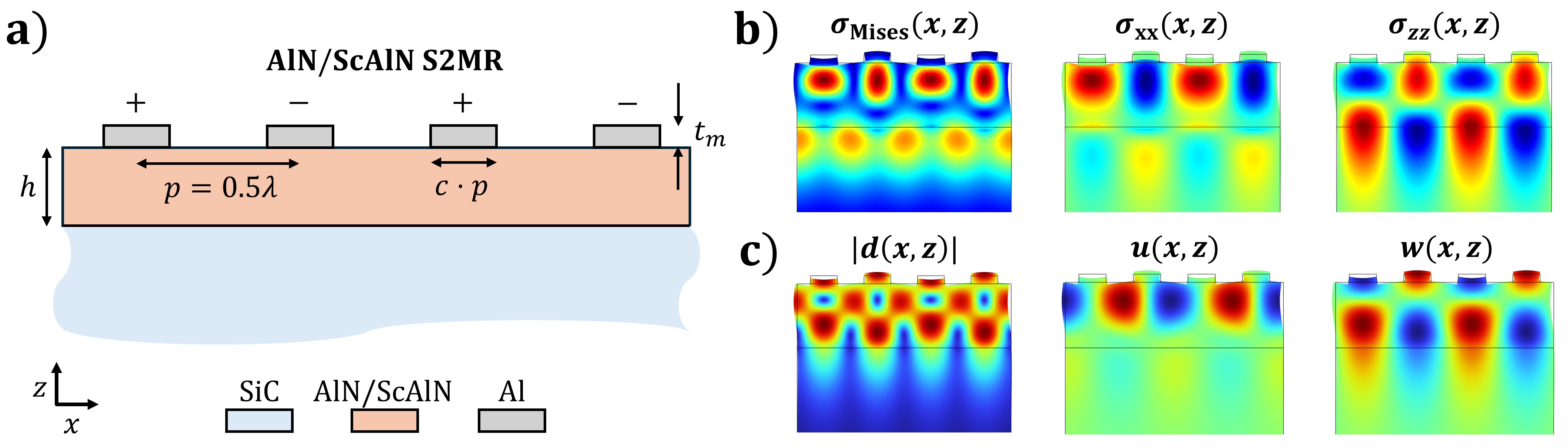
The embodiment of the proposed Scandium Aluminum Nitride (ScAlN) nanoacoustic Solidly-Mounted Bidimensional Resonators (S2MR) consists of a thin film () of piezoelectric material solidly-mounted on a fast, bulk substrate of Silicon Carbide (SiC) with patterned metallic Interdigitated Transducers (IDTs) spaced by half acoustic wavelength () on the top surface (Fig. 1a). From a physical perspective, S2MRs are slow, dispersive Surface Acoustic Wave (SAW) devices exploiting a highly-optimized Sezawa mode [21][22][23] on a substrate with high propagation velocity (). Similarly to Cross-Sectional Lamé Mode Resonators (CLMRs), they exploit both the and piezoelectric coefficient to generate a bidimensional acoustic standing wave with significant stress and displacement components in the lateral () and thickness () directions, as confirmed by COMSOL® Multiphysics Finite Element Analysis (FEA) simulations (Fig. 1b-c). The large acoustic impedance mismatch between the active layer and the substrate is pivotal in constraining the acoustic energy into the piezoelectric medium, hence ensuring the existence of the resonant mode with large quality factor () and electromechanical coupling (). Metal-metal and metal-insulator layered Bragg reflectors [24], sapphire [25], silicon carbide [26], and diamond [27] substrates exhibit mechanical properties suitable for sustaining S2MRs in Sc-doped AlN.
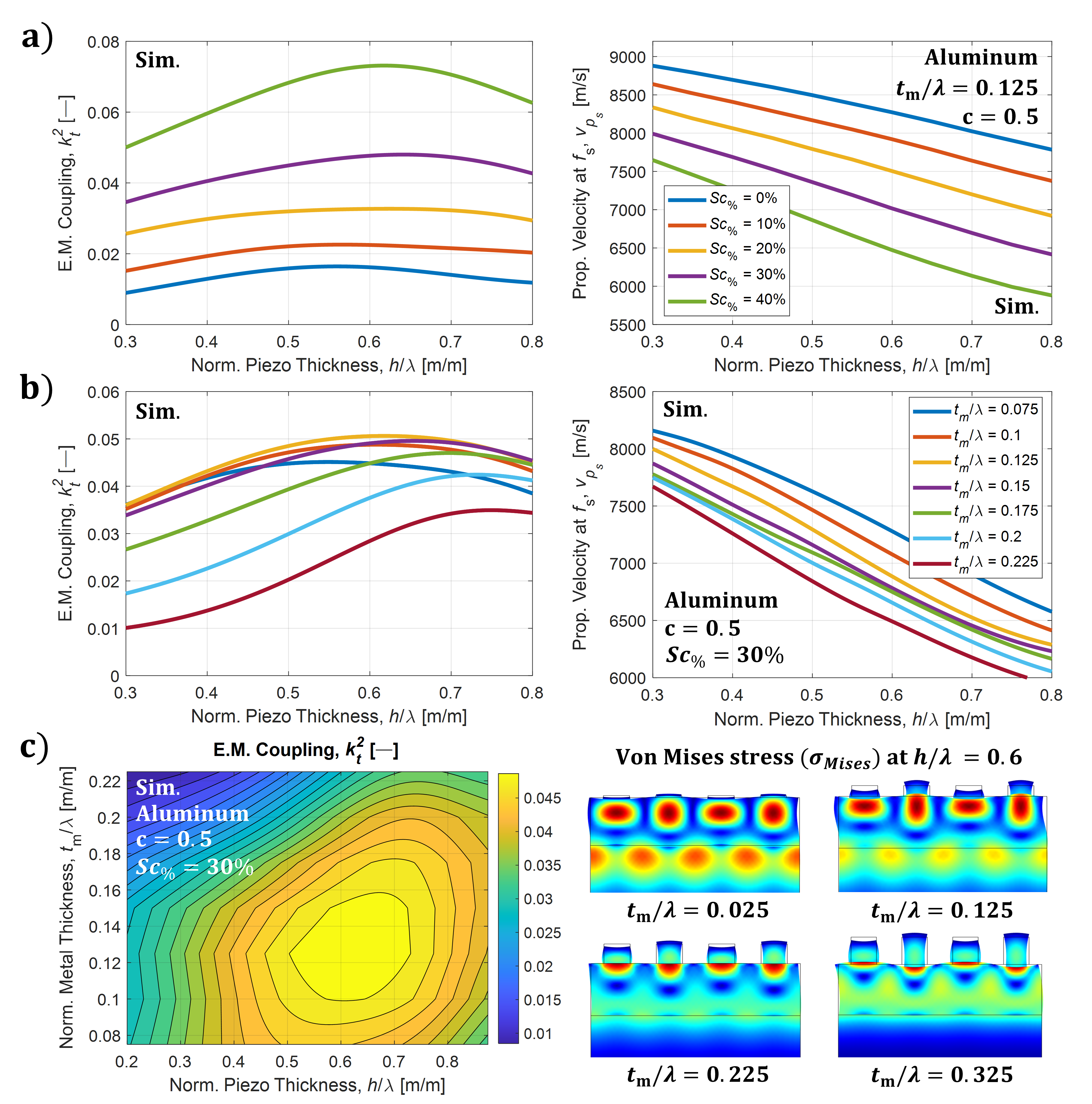
Finite element analysis (FEA) simulations based on the a priori material properties of ScAlN, as described by Caro et al. [28], reveal a super linear growth in at higher levels of Sc-doping (). This behavior is attributed to the combined effects of increased piezoelectric coefficients and a reduction in propagation velocity (Fig. 2a). Despite the presence of a local maxima for an of 0.6, this class of devices retains sub-optimal, large coupling over a broad range of , thus enabling single-step, lithographic multi-frequency definition for the synthesis of on-chip acoustic filter banks [19]. Ultimately, S2MRs require tailored electrode material-thickness () optimization to maximize the coupling between the electric field laterally excited by the IDTs [29] and the Sezawa’s mode induced acoustic strain field. As reported in Figs. 2b-c, , and must be co-optimized for a given IDT material, coverage (), and , to ensure ideal energy localization in the piezoelectric medium.
In this work, 30%-doped AlN-seeded ScAlN, 6H-SiC, and patterned aluminum (Al) with a 50% metallization ratio () are implemented as the active layer, fast substrate, and IDT metal, respectively. While the material selection is primarily driven by established fabrication processes [19], the choice of the fast substrate hints at the potential for future monolithic integration of RF acoustic front-ends with high-power electronics, tailored for military and harsh-environment applications. According to the FEA simulations reported in Fig. 2b, is set to 250 nm, to 50 nm, and to 400 nm to target a frequency of operation () of 16 GHz and maximized coupling.
3 Fabrication
The fabrication process adopted for the S2MRs manufacturing is illustrated in Fig. 3a. The process begins with the in-house deposition of a 230 nm layer of 30% ScAlN onto a 4-inch SiC substrate via reactive sputtering, using a commercial-grade Evatec CLUSTERLINE® 200 II system and a 12-inch casted target. The ScAlN thin film is sputtered onto a pre-deposited 20 nm-thick AlN seed layer [30], which serves as a templated nucleation layer to promote the growth of highly crystalline, -axis-oriented piezoelectric films [31].
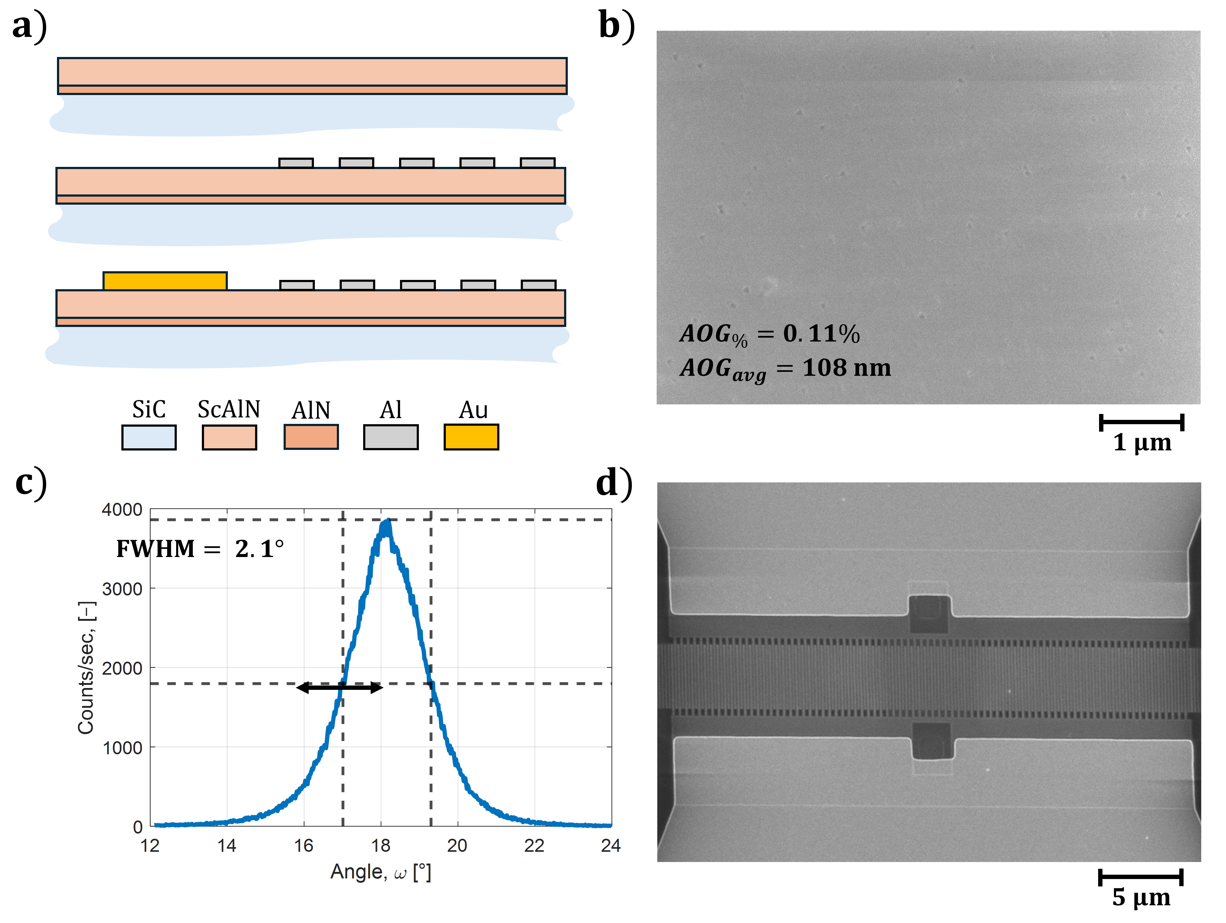
Characterization using Scanning Electron Microscope (SEM), Abnormally Oriented Grain (AOG) surface density () and average dimension () evaluation [32], as well as X-Ray Diffraction (XRD) Full Width Half Maximum (FWHM) measurements confirmed state-of-the-art crystallinity. The results show an almost AOG-free top surface ( = 0.11% and = 108 nm) and a Rocking Curve (RC) of 1.5°(Figs. 3b-c).
Subsequently, Interdigital Transducers (IDTs) are defined via e-beam lithography, necessitated by the critical feature size of 100 nm. A 50 nm thin film is deposited through thermal evaporation, followed by an overnight lift-off in 1165 Microposit remover. Finally, pads and interconnects are patterned using thermal evaporation of 250 nm of gold (Au), followed by a lift-off process.
4 Results and Discussion
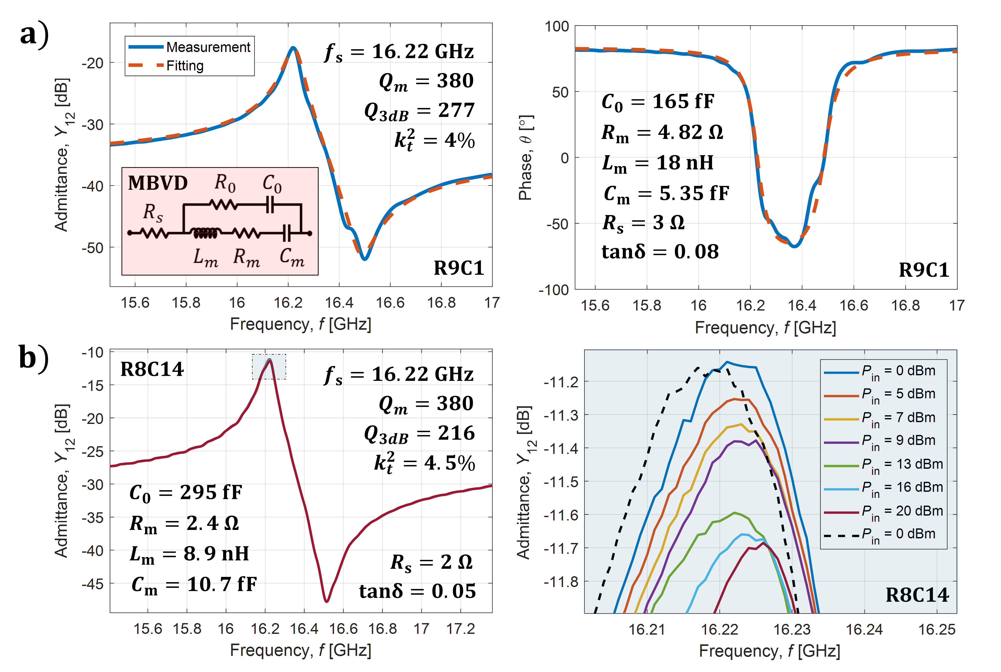
The fabricated devices are characterized under laboratory conditions ( = 293 K) with 150 GSG probes in a two-port configuration to extract their characteristics frequency response. Scattering () parameters are measured with a vector network analyzer (Keysight P5008A) and later converted into admittance () parameters via software. The equivalent circuit parameters are extracted by fitting the transmission admittance () response to a Modified Butterworth-Van Dyke (MBVD) equivalent model [33]. The admittance of the device exhibiting the largest 3-dB quality factor () is reported in Fig. 3a, demonstrating a of 277, a motional quality factor of , and of 4%, for an overall Figure of Merit () slightly exceeding 14. Power handling characterization is performed on a separate device, most closely matched to 50 , possessing similar quality factor ( = 380 and = 216) and the highest measured coupling () and Figure of Merit ( = 17). Fig. 3b shows the admittance response as the input power is swept from 0 dBm to the maximum power permitted by the setup (20 dBm), and then returned to the baseline of 0 dBm. A close-up of the resonant peak reveals minimal admittance degradation across the investigated input power range and no permanent deterioration of the quality factor upon returning to baseline. A first-order Temperature Coefficient of Frequency () of -40 ppm/K is finally inferred from temperature testing between 293 and 393 K [19]. To the best of the authors’ knowledge, S2MRs exhibit the highest Key Performance Indicators (KPIs) among solidly mounted resonators in the Ku band, paving the way for the monolithic integration of nanoacoustic devices with high-power electronics on SiC for commercial, military, and harsh-environment applications requiring sharp frequency selectivity and high power handling.
References
- [1] J. D. Dunworth, A. Homayoun, B.-H. Ku, Y.-C. Ou, K. Chakraborty, G. Liu, T. Segoria, J. Lerdworatawee, J. W. Park, H.-C. Park, H. Hedayati, D. Lu, P. Monat, K. Douglas, and V. Aparin, “A 28GHz Bulk-CMOS dual-polarization phased-array transceiver with 24 channels for 5G user and basestation equipment,” in 2018 IEEE International Solid-State Circuits Conference - (ISSCC), pp. 70–72, Feb. 2018. 10.1109/ISSCC.2018.8310188.
- [2] Y. Zhong, Y. Yang, X. Zhu, E. Dutkiewicz, K. M. Shum, and Q. Xue, “An On-Chip Bandpass Filter Using a Broadside-Coupled Meander Line Resonator With a Defected-Ground Structure,” IEEE Electron Device Letters, vol. 38, pp. 626–629, May 2017.
- [3] R. Aigner, G. Fattinger, M. Schaefer, K. Karnati, R. Rothemund, and F. Dumont, “BAW Filters for 5G Bands,” in 2018 IEEE International Electron Devices Meeting (IEDM), pp. 14.5.1–14.5.4, Dec. 2018.
- [4] M. Matthaiou, O. Yurduseven, H. Q. Ngo, D. Morales-Jimenez, S. L. Cotton, and V. F. Fusco, “The Road to 6G: Ten Physical Layer Challenges for Communications Engineers,” IEEE Communications Magazine, vol. 59, pp. 64–69, Jan. 2021. 10.1109/MCOM.001.2000208.
- [5] G. Gültepe, T. Kanar, S. Zihir, and G. M. Rebeiz, “A 1024-Element Ku-Band SATCOM Dual-Polarized Receiver With >10-dB/K G/T and Embedded Transmit Rejection Filter,” IEEE Transactions on Microwave Theory and Techniques, vol. 69, pp. 3484–3495, July 2021.
- [6] M. Alexandru, V. Banu, J. Montserrat, P. Godignon, and J. Millán, “Monolithic Integration of High Temperature Silicon Carbide Integrated Circuits,” ECS Transactions, vol. 58, p. 375, Aug. 2013. 10.1149/05804.0375ecst.
- [7] S. Yuvaraja, V. Khandelwal, X. Tang, and X. Li, “Wide bandgap semiconductor-based integrated circuits,” Chip, vol. 2, p. 100072, Dec. 2023. 10.1016/j.chip.2023.100072.
- [8] Y. Zheng and W. Sheng, “Compact Lumped-Element LTCC Bandpass Filter for Low-Loss VHF-Band Applications,” IEEE Microwave and Wireless Components Letters, vol. 27, pp. 1074–1076, Dec. 2017. 10.1109/LMWC.2017.2754338.
- [9] J.-X. Xu, X. Y. Zhang, X.-L. Zhao, and Q. Xue, “Synthesis and Implementation of LTCC Bandpass Filter With Harmonic Suppression,” IEEE Transactions on Components, Packaging and Manufacturing Technology, vol. 6, pp. 596–604, Apr. 2016. 10.1109/TCPMT.2016.2531180.
- [10] X. Du, M. H. Idjadi, Y. Ding, T. Zhang, A. J. Geers, S. Yao, J. B. Pyo, F. Aflatouni, M. Allen, and R. H. Olsson, “Frequency tunable magnetostatic wave filters with zero static power magnetic biasing circuitry,” Nature Communications, vol. 15, p. 3582, Apr. 2024. 10.1038/s41467-024-47822-3.
- [11] A. Kochhar, R. Vetury, J. Leathersich, Z. Schaffer, C. Moe, D. Kim, K. Cheema, M. Winters, and J. Shealy, “X-band Bulk Acoustic Wave Resonator (XBAW) using Periodically Polarized Piezoelectric Films (P3F),” in 2023 IEEE International Ultrasonics Symposium (IUS), pp. 1–4, Sept. 2023. 10.1109/IUS51837.2023.10306825.
- [12] T. Takai, H. Iwamoto, Y. Takamine, T. Fuyutsume, T. Nakao, M. Hiramoto, T. Toi, and M. Koshino, “I.H.P. SAW technology and its application to microacoustic components (Invited),” in 2017 IEEE International Ultrasonics Symposium (IUS), pp. 1–8, Sept. 2017. 10.1109/ULTSYM.2017.8091876.
- [13] T. Takai, H. Iwamoto, Y. Takamine, T. Fuyutsume, T. Nakao, M. Hiramoto, T. Toi, and M. Koshino, “High-Performance SAW Resonator With Simplified LiTaO3/SiO2 Double Layer Structure on Si Substrate,” IEEE Transactions on Ultrasonics, Ferroelectrics, and Frequency Control, vol. 66, pp. 1006–1013, May 2019. 10.1109/TUFFC.2019.2898046.
- [14] R. Ruby, “A decade of FBAR success and what is needed for another successful decade,” in 2011 Symposium on Piezoelectricity, Acoustic Waves and Device Applications (SPAWDA), pp. 365–369, Dec. 2011. 10.1109/SPAWDA.2011.6167265.
- [15] A. Hagelauer, R. Ruby, S. Inoue, V. Plessky, K.-Y. Hashimoto, R. Nakagawa, J. Verdu, P. d. Paco, A. Mortazawi, G. Piazza, Z. Schaffer, E. T.-T. Yen, T. Forster, and A. Tag, “From Microwave Acoustic Filters to Millimeter-Wave Operation and New Applications,” IEEE Journal of Microwaves, vol. 3, pp. 484–508, Jan. 2023. 10.1109/JMW.2022.3226415.
- [16] R. Vetury, A. S. Kochhar, and J. B. Shealy, “XBAW, An Enabling Technology for Next Generation Resonators and Filter Solutions for 5G and Wi-Fi 6/6E/7 applications (Invited),” in 2022 International Electron Devices Meeting (IEDM), pp. 16.1.1–16.1.4, Dec. 2022. 10.1109/IEDM45625.2022.10019537.
- [17] J. Kramer, S. Cho, M. E. Liao, K. Huynh, O. Barrera, L. Matto, M. S. Goorsky, and R. Lu, “57 GHz Acoustic Resonator with of 7.3% and Q of 56 in Thin-Film Lithium Niobate,” in 2022 International Electron Devices Meeting (IEDM), pp. 16.4.1–16.4.4, Dec. 2022. 10.1109/IEDM45625.2022.10019391.
- [18] G. Giribaldi, L. Colombo, M. Castellani, M. A. Masud, G. Piazza, and M. Rinaldi, “Up-Scaling Microacoustics: 20 to 35 GHz ALN Resonators with f • Q Products Exceeding 14 THz,” in 2024 IEEE 37th International Conference on Micro Electro Mechanical Systems (MEMS), pp. 31–35, Jan. 2024. 10.1109/MEMS58180.2024.10439371.
- [19] G. Giribaldi, L. Colombo, P. Simeoni, and M. Rinaldi, “Compact and wideband nanoacoustic pass-band filters for future 5G and 6G cellular radios,” Nature Communications, vol. 15, p. 304, Jan. 2024. 10.1038/s41467-023-44038-9.
- [20] X. Du, N. Sharma, Z. Tang, C. Leblanc, D. Jariwala, and R. H. Olsson, “Near 6-GHz Sezawa Mode Surface Acoustic Wave Resonators Using AlScN on SiC,” Journal of Microelectromechanical Systems, vol. 33, pp. 577–585, Oct. 2024. 10.1109/JMEMS.2024.3430984.
- [21] I. Ahmed, U. Rawat, J.-T. Chen, and D. Weinstein, “Super-High-Frequency Low-Loss Sezawa Mode SAW Devices in a GaN/SiC Platform,” IEEE Transactions on Ultrasonics, Ferroelectrics, and Frequency Control, vol. 70, pp. 291–301, Apr. 2023.
- [22] F. Hadj-Larbi and R. Serhane, “Sezawa SAW devices: Review of numerical-experimental studies and recent applications,” Sensors and Actuators A: Physical, vol. 292, pp. 169–197, June 2019. 10.1016/j.sna.2019.03.037.
- [23] K. Sezawa, “Dispersion of Elastic Waves propagated on the Surface of Stratified Bodies and on Curved Surfaces,” Sept. 1927.
- [24] O. Barrera, N. Ravi, K. Saha, S. Dasgupta, J. Campbell, J. Kramer, E. Kwon, T.-H. Hsu, S. Cho, I. Anderson, P. Simeoni, J. Hou, M. Rinaldi, M. S. Goorsky, and R. Lu, “18 GHz Solidly Mounted Resonator in Scandium Aluminum Nitride on SiO2/Ta2O5Bragg Reflector,” Journal of Microelectromechanical Systems, pp. 1–0, 2024. 10.1109/JMEMS.2024.3472615.
- [25] J. Guida, G. Giribaldi, L. Colombo, M. Rinaldi, and S. Ghosh, “Solidly Mounted Two-Dimensional Guided Modes in 30% Scandium Aluminum Nitride on Sapphire,” in 2023 22nd International Conference on Solid-State Sensors, Actuators and Microsystems (Transducers), pp. 2094–2097, June 2023.
- [26] L. Colombo, G. Giribaldi, J. Guida, S. Ghosh, C. Cassella, and M. Rinaldi, “Solidly Mounted Bi-dimensional Mode Resonators,” Oct. 2024. US20240356527A1.
- [27] S. Fujii, T. Haruki, and Y. Shiba, “Diamond SAW Resonator,” in 2020 4th Australian Microwave Symposium (AMS), pp. 1–2, Feb. 2020.
- [28] M. A. Caro, S. Zhang, T. Riekkinen, M. Ylilammi, M. A. Moram, O. Lopez-Acevedo, J. Molarius, and T. Laurila, “Piezoelectric coefficients and spontaneous polarization of ScAlN,” Journal of Physics. Condensed Matter: An Institute of Physics Journal, vol. 27, p. 245901, June 2015. 10.1088/0953-8984/27/24/245901.
- [29] T. Murata, M. Kadota, T. Nakao, K. Matsuda, and K.-y. Hashimoto, “Improvement of Shape Factor and Loss of Surface Acoustic Wave Resonator Filter Composed of SiO2/High-Density-Electrode/LiTaO3,” Japanese Journal of Applied Physics, vol. 48, p. 07GG05, July 2009. Publisher: IOP Publishing.
- [30] M. T. Hardy, A. C. Lang, E. N. Jin, N. Nepal, B. P. Downey, V. J. Gokhale, D. Scott Katzer, and V. D. Wheeler, “Nucleation control of high crystal quality heteroepitaxial Sc0.4Al0.6N grown by molecular beam epitaxy,” Journal of Applied Physics, vol. 134, p. 105301, Sept. 2023. 10.1063/5.0164430.
- [31] R. D. Felice, J. E. Northrup, and J. Neugebauer, “Energetics of AlN thin films and the implications for epitaxial growth on SiC,” Physical Review B, vol. 54, pp. R17351–R17354, Dec. 1996. 10.1103/PhysRevB.54.R17351.
- [32] L. Spagnuolo, L. Colombo, W. Gubinelli, K. Saha, P. Simeoni, and M. Rinaldi, “An Image Recognition Technique for The Quantitative Analysis of Abnormally Oriented Grains in Advanced Piezoelectric Material,” in 2024 IEEE Ultrasonics, Ferroelectrics, and Frequency Control Joint Symposium, Nov. 2024.
- [33] J. Larson, P. Bradley, S. Wartenberg, and R. Ruby, “Modified Butterworth-Van Dyke circuit for FBAR resonators and automated measurement system,” in 2000 IEEE Ultrasonics Symposium. Proceedings. An International Symposium (Cat. No.00CH37121), vol. 1, pp. 863–868 vol.1, Oct. 2000. 10.1109/ULTSYM.2000.922679.