capbtabboxtable[\FBwidth]
Solving the Inverse Band-Structure Problem for Photonic Crystals
Abstract
We present a symmetry-agnostic topology optimization framework for photonic-crystal structures based on computation of the photonic density of states in a manner analogous to -point integration. We provide a generalization of the approach that allows for computations at different scales with the additional scales being analogous to integration over the full Brillouin zone and to regimes between the two limiting cases of full Brillouin-zone integration and -point integration, though these other scales do not preserve the symmetry-agnostic nature of the -point framework. We also demonstrate how our approach can be generalized to the problem of inverting photonic or phononic bandstructures. Finally, we show that at the symmetry-agnostic scale analogous to -point integration, we can recover a known two-dimensional photonic crystal for the TM polarization. A key insight of our work is the determination of the minimum supercell size and the minimum precision to which the frequencies within the photonic bandgap must be sampled in order to observe photonic-crystal structures.
Regarding circuits based on semiconductor technology, increased miniaturization is leading to circuits with higher resistance and higher levels of power dissipation Joannopoulos et al. (1997); Shalf (2020). Photonic systems outperform electronic systems for low-loss, high-capacity transmission of information Agrawal (2012); Winzer et al. (2018), which suggests that fabrication of the analog of a transistor for photonic systems would have the potential to revolutionize the information technology industry Joannopoulos et al. (1997). The difficulty lies in robustly designing structures, known as photonic crystals, with photonic bandgaps, as these structures would require feature sizes of less than 1 m for their regime of operation Joannopoulos et al. (1997); Men et al. (2014). In recent decades, significant advances have been made in the design of nanophotonic structures, including of photonic crystals, as well as in the determination of bounds on the optimal performance of nanophotonic devices Jensen and Sigmund (2011); Molesky et al. (2018); Li et al. (2019); Chao et al. (2022a). Optimizing the distribution of material within a nanophotonic device, as captured by the value of the permittivity throughout the design region, was initially accomplished by designing structures by hand or by varying a few parameters to find an optimal solution Maldovan and Thomas (2004); Joannopoulos et al. (2011); Fan et al. (1994); Doosje et al. (2000); Biswas et al. (2002); Maldovan et al. (2002); Toader et al. (2003); Michielsen and Kole (2003); Maldovan et al. (2003); Maldovan and Thomas (2005). Later efforts involved level-set descriptions Kao et al. (2005); Burger et al. (2004); Burger and Osher (2005); He et al. (2007) and continuous relaxations of Dobson and Cox (1999); Cox and Dobson (2000); Shen et al. (2002); Halkjær et al. (2006); Sigmund and Hougaard (2008); Sigmund and Jensen (2003); Jensen and Sigmund (2004); Watanabe et al. (2006); Liang and Johnson (2013), where every pixel or voxel is allowed to vary continuously within some range , an approach we adopt in this work though it is not integral to our framework. The optimization algorithms include gradient-based approaches Cox and Dobson (2000); Kao et al. (2005); Dobson and Cox (1999), which we employ in this work for illustrative purposes though employing gradient descent is again not integral to the framework, semidefinite programming Men et al. (2010, 2014), and gradient-free techniques Goh et al. (2007); Yan et al. (2021); Kim et al. (2023). Invariably, the previous approaches to optimizing photonic crystals have involved consideration of the photonic bandstructure for a given crystal lattice of a fixed symmetry and optimization of the gap between consecutive bands in the bandstructure. Such approaches are limited in that, unless an exhaustive search of all possible crystal symmetries is conducted, there is the possibility of missing a design that is more optimal than the ones found for the explored symmetries.
Our approach addresses this shortcoming of previous approaches through a formalism that is able to discover crystals of arbitrary symmetry by minimizing the photonic density of states over a frequency window with central frequency for a sufficiently large design region supercell using a framework analogous to -point integration. A key insight of our work is the determination of the minimum supercell size and the minimum precision to which the frequency window must be sampled in order to observe photonic-crystal structures.
Results
Photonic-crystal convergence as a function of system size
We now present results for two-dimensional structures supporting photonic bandgaps for the transverse magnetic (TM) polarization that were obtained by suppressing the photonic density of states of the structures over a frequency window with a central frequency , where the photonic density of states is computed in a manner analogous to -point integration. For all TM calculations, we assigned the values , , for the permeability, and allowed the permittivity to vary between and for comparison with the structures found in Ref. Joannopoulos et al. (2011). The quantities , , and are the speed of light, the permeability, and the permittivity for free space, respectively, and we set since we can treat lengths without dimensions given the scale invariance of Maxwell’s equations Joannopoulos et al. (2011). Convergence of the photonic crystal as a function of the system size and the grid-point resolution (gpr), which is the number of grid points used to resolve a length , is shown for the TM polarization in Fig. 1. By performing a Fourier transform of the structure that was optimized over 5000 iterations for a design region, a gpr of 100, and , where is the number of frequencies sampled within the bandgap, we can extract the location of the four highest maxima of the absolute value of the transform that occur at non-trivial positions. We find that these maxima are located at , , , and . Observing that the real-space structure of the photonic crystal with and a design region at 5000 iterations corresponds to dielectric columns/rods, we can extract the radius of these rods by summing the absolute value of the Fourier transform at the locations , , , and , dividing by (which is the number of effective unit cells given the location of the maxima of the absolute value of the Fourier transform), dividing by , and then taking the square root. We obtain , where , compared with the value in Ref. Joannopoulos et al. (2011) which was for some lattice constant .
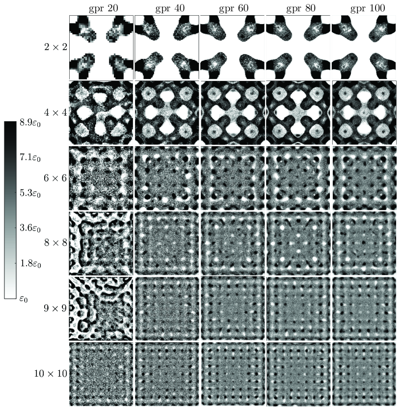
The convergence as a function of system size can be understood by observing that the Bragg length, which dictates the characteristic length for attenuation of light illuminating a photonic crystal, varies as Hasan et al. (2018); Neve-Oz et al. (2004)
| (1) |
where is the central frequency, is the bandgap or frequency window, as above, and is the smallest distance for a set of crystal planes. Thus, given and , we expect a minimum crystal linear dimension of for convergence of the results, in good agreement with the convergence behavior in Fig. 1.
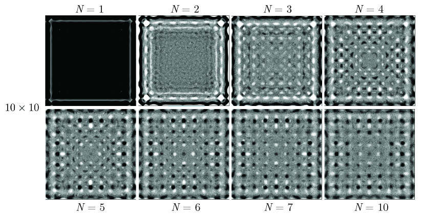
Convergence as a function of the number of frequencies, , sampled within the bandgap
We next examine the photonic-crystal convergence behavior as a function of for TM polarization. As shown in Fig. 2, we find that photonic-crystal behavior is not captured for all . The location of the crossover point to the final TM photonic-crystal structure can be understood by observing that each sampled frequency , within the bandgap, is in correspondence with a wavenumber , where is the speed of light through the given medium. These wavenumbers must be able to capture the length scales of all structures in the photonic crystal. In particular, they must be able to capture the length scale corresponding to the periodicity of the photonic crystal. We treat time-harmonic fields so that we can use the rules for addition of sinusoidal functions to deduce that the smallest difference between these must be equal to the smallest wavenumber at which a peak is observed in the Fourier transform of the optimized structure. This argument follows from the fact that the function resulting from the sum of sinusoidal functions is a product of an envelope function with frequency equal to the smaller of the difference between or the sum of the frequencies of the original sinusoidal functions and a modulated sinusoidal function with frequency equal to the larger of the difference between or the sum of the frequencies of the original sinusoidal functions. Given a smallest wavenumber , we find a minimum given by for a gpr of 100, , , and using , in good agreement with the results shown in Fig. 2.
Extracting photonic bandstructures
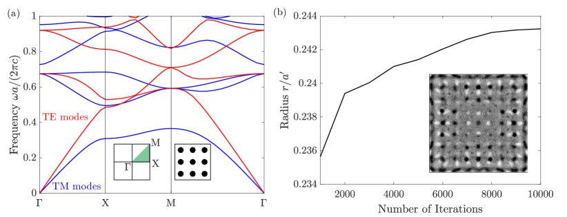
As a function of the number of iterations, we also investigate the convergence of the radius that was computed above at 5000 iterations for the photonic-crystal structure resulting from minimization of the photonic density of states over the frequency window with central frequency for a design region, , and a gpr of 100. The location of the four highest maxima of the absolute value of the Fourier transform occurring at non-trivial positions for the photonic-crystal structures does not change between 1000 and 10000 iterations, We find that between 9000 and 10000 iterations, the relative change in the radius is less than 0.03%. For the radius obtained at 10000 iterations, which we also found to be , we compute the corresponding bandstructure using the MPB code Johnson and Joannopoulos (2001). Given that the lattice constant in the computation is increased by a factor of , based on the periodicity of the structure that we found compared to , we need to rescale the frequencies we obtain by the factor if we are to use the lattice constant . The bandstructure is shown in Fig. 3. After this rescaling, we find and . The value of is in good agreement with our input value of , which indicates that our optimization procedure is able to target a desired bandgap regime. The value of obtained is also consistent with our input that requested that the bandgap be at least as large as .
Discussion
Overall, we have presented an approach to the optimization of photonic crystals that does not require the specification of any particular symmetry or an exhaustive search over all possible symmetries to discover the optimal design. This approach is based on optimization of the photonic density of states over a sufficiently large design region supercell in a manner analogous to -point integration. We have shown that we can capture a known structure for a two-dimensional photonic crystal with the TM polarization using the symmetry-agnostic calculation regime that is analogous to -point integration. The key to the observation of the TM photonic crystal is our determination of the minimum supercell size and the minimum precision to which the bandgap must be sampled.
Methods
Deriving the photonic-crystal objective
In order to create structures with photonic bandgaps, which are ranges of frequencies for which no electromagnetic wave can penetrate the structure, we first observe that the existence of a photonic bandgap is equivalent to the suppression of the photonic density of states (DOS) over the frequency window . In order to obtain the photonic DOS, we start with the per-polarization photonic local density of states (LDOS), which is related to the power radiated by a point dipole, that is a current where is the unit vector in the dipole’s direction, is the position of the dipole, is a Dirac delta function that integrates to unity if lies within the region of integration and zero otherwise, and is the frequency of the dipole, in the following manner Liang and Johnson (2013); D’Aguanno et al. (2004); Novotny and Hecht (2012); Inoue and Ohtaka (2004); Martin and Piller (1998); Taflove et al. (2013),
| (2) |
The electric field appearing in Eq. (2) is obtained by inverting the equation
| (3) |
where
| (4) |
is the Maxwell operator with and being the permeability and permittivity in the design region, respectively, and
| (5) |
Once the per-polarization LDOS has been obtained, the DOS is obtained by summing the LDOS over the relevant polarizations and integrating over the entire crystal Taflove et al. (2013),
| (6) |
The next step is to apply a finite-bandwidth formalism Shim et al. (2019); Liang and Johnson (2013) for optimizing the DOS. Explicitly, we integrate over all frequencies the complex DOS (DOS′) multiplied by a window function that has the form,
| (7) |
for some normalization constant , some central frequency , some bandwidth which we will also refer to as the bandgap , and some integer , which was defined above as the number of frequencies sampled within the bandgap. This window function approaches a rectangular function as . After the integration of the complex DOS given by
| (8) |
we extract the real part again Shim et al. (2019); Liang and Johnson (2013). Applying Cauchy’s residue theorem we obtain
| (9) | ||||
| (10) |
Above, we do not include the pole at since we consider moderate bandwidths Chao et al. (2022b); Strekha et al. (2024). The procedure is then to minimize the quantity .
Point-dipole approach
There are at least three ways to approach the problem of computing the . The first is computationally intensive, but would allow for features of arbitrary size in the photonic crystal to be resolved. The approach involves inverting Eq. (3) for each frequency and for a number of dipoles, , equal to the number of pixels or voxels in the design region multiplied by the number of relevant polarizations. There is in principle some inefficiency in such inversions because we really only need the electric field from a given dipole at the location of the dipole. Effectively, to be able to treat all the dipoles needed in the construction of the simultaneously, we would need to be able to operate on a uniform array of dipoles covering the entire design region with the diagonal part of the inverse of the sparse Maxwell operator, that is with the diagonal part of the Green’s function, . Since the current vector is composed of point dipoles that integrate to unity, for a single polarization this approach to computing the amounts to computing the trace of multiplied by and to taking the imaginary part after integrating its product with the window function over all frequencies Hasan et al. (2018); Sprik et al. (1996); Busch and John (1998); Chao et al. (2022b). Explicitly,
| (11) |
This result follows from the fact that
| (12) |
To our knowledge, there does not exist a sufficiently efficient approach for evaluating the trace of the Green’s function for a large sparse Maxwell operator. Indeed, this approach becomes computationally intractable for all but the smallest system sizes, for which the results are not physically meaningful as we saw above.
Uniform-source approach
The second approach is less computationally intensive, but is only approximately correct in the far-field region and for small to moderate bandwidths, and therefore cannot resolve very fine features. This second approach involves inverting Eq. (3) once for each frequency and for each relevant polarization, but for uniform currents, , covering every pixel or voxel in the design region. The reason this approach can give reasonable results in the far-field region ( ) is that for moderate bandwidths the electric field scales approximately as Jackson (1999) , where the wavenumber, , depends on the frequency , is the unit vector in the direction of , and is the unit vector in the direction of the electric dipole moment . This electric dipole moment is obtained as
| (13) |
where is obtained through
| (14) |
and where we consider the Kronecker delta contribution, , to a given uniform current, , from each position separately. Summing the electric fields emanating from the location for each of the frequencies leads to the resulting field scaling as in the limit where , where is the Kronecker delta that is equal to 1 when and 0 otherwise and where we have used the relation as . Ultimately, the electric field effectively behaves as if we had found the diagonal elements of the inverse of the Maxwell operator and acted on the uniform currents with the operator consisting of those diagonal elements, which is what we desired above.
To obtain the electric fields for TM polarization, we treat the structure to optimize as varying in the plane with a single uniform current, , and use the ceviche code for the scalar electric field Hughes et al. (2019) with the NLopt package Johnson (2007) employing the Method of Moving Asymptotes (MMA) algorithm Svanberg (2002). The structure and source are understood to be uniform in the direction, which we neglect in the integrations.
Mixed-regime sources
The third approach involves combining the point-dipole approach and the uniform-source approach. Explicitly, we consider sources , where the are chosen from among some set of vectors and the positions are chosen from among the set of all the positions in the design region that do not create equivalent . This form for the sources captures evenly sampling from sources with periodicities specified by the vectors, where each vector can be understood to represent a wavevector. Again, Eq. (3) must be inverted for all relevant polarizations. The point-dipole approach and the uniform-source approach are limiting cases of this method. For the point-dipole approach the vectors cover the entire Brillouin zone of the space that is reciprocal to the real-space design region and the approach is analogous to integrating over the full Brillouin zone of reciprocal space. For the uniform-source approach, there is a single vector , which is analogous to -point integration. We note that only for a single vector is the symmetry-agnostic nature of our approach fully preserved.
Inverting bandstructures
We note also that our framework readily generalizes to the solution of the problem of inverting a photonic bandstructure for a given crystal symmetry, and could also apply to solving the problem of inverting a phononic bandstructure for a particular crystal symmetry given the similarities in the structure of the equations for the two problems. In order to invert the photonic bandstructure, one would simply compute the Fourier transform of the LDOS and suppress the resulting quantity at every frequency and wavevector in the bandstructure diagram where a band does not exist. Explicitly, one would suppress the quantity,
| (15) |
at every wavevector and every frequency where a band does not exist.
ACKNOWLEDGMENTS:
R.K.D. acknowledges financial support that made this work possible from the National Academies of Science, Engineering, and Medicine Ford Foundation Postdoctoral Fellowship program and from a startup package provided by Syracuse University. The authors also acknowledge that the work reported on in this paper was substantially performed using Zest, the Syracuse University research computing high-performance computing cluster. Finally, we wish to acknowledge fruitful conversations with Benjamin Strekha, Pengning Chao, and Alejandro W. Rodriguez.
References
- Joannopoulos et al. (1997) J. D. Joannopoulos, P. R. Villeneuve, and S. Fan, Nature 386, 143 (1997).
- Shalf (2020) J. Shalf, Philosophical Transactions of the Royal Society A 378, 20190061 (2020).
- Agrawal (2012) G. Agrawal, Fiber-Optic Communication Systems, Wiley Series in Microwave and Optical Engineering (Wiley, 2012).
- Winzer et al. (2018) P. J. Winzer, D. T. Neilson, and A. R. Chraplyvy, Opt. Express 26, 24190 (2018).
- Men et al. (2014) H. Men, K. Y. Lee, R. M. Freund, J. Peraire, and S. G. Johnson, Optics express 22, 22632 (2014).
- Jensen and Sigmund (2011) J. S. Jensen and O. Sigmund, Laser & Photonics Reviews 5, 308 (2011).
- Molesky et al. (2018) S. Molesky, Z. Lin, A. Y. Piggott, W. Jin, J. Vučković, and A. W. Rodriguez, Nature Photonics 12, 659 (2018).
- Li et al. (2019) W. Li, F. Meng, Y. Chen, Y. f. Li, and X. Huang, Advanced Theory and Simulations 2, 1900017 (2019).
- Chao et al. (2022a) P. Chao, B. Strekha, R. Kuate Defo, S. Molesky, and A. W. Rodriguez, Nature Reviews Physics 4, 543 (2022a).
- Maldovan and Thomas (2004) M. Maldovan and E. L. Thomas, Nature Materials 3, 593 (2004).
- Joannopoulos et al. (2011) J. Joannopoulos, S. Johnson, J. Winn, and R. Meade, Photonic Crystals: Molding the Flow of Light - Second Edition (Princeton University Press, 2011).
- Fan et al. (1994) S. Fan, P. R. Villeneuve, R. D. Meade, and J. D. Joannopoulos, Applied Physics Letters 65, 1466 (1994).
- Doosje et al. (2000) M. Doosje, B. J. Hoenders, and J. Knoester, J. Opt. Soc. Am. B 17, 600 (2000).
- Biswas et al. (2002) R. Biswas, M. M. Sigalas, K.-M. Ho, and S.-Y. Lin, Phys. Rev. B 65, 205121 (2002).
- Maldovan et al. (2002) M. Maldovan, A. M. Urbas, N. Yufa, W. C. Carter, and E. L. Thomas, Phys. Rev. B 65, 165123 (2002).
- Toader et al. (2003) O. Toader, M. Berciu, and S. John, Phys. Rev. Lett. 90, 233901 (2003).
- Michielsen and Kole (2003) K. Michielsen and J. S. Kole, Phys. Rev. B 68, 115107 (2003).
- Maldovan et al. (2003) M. Maldovan, C. K. Ullal, W. C. Carter, and E. L. Thomas, Nature Materials 2, 664 (2003).
- Maldovan and Thomas (2005) M. Maldovan and E. L. Thomas, J. Opt. Soc. Am. B 22, 466 (2005).
- Kao et al. (2005) C. Y. Kao, S. Osher, and E. Yablonovitch, Applied Physics B 81, 235 (2005).
- Burger et al. (2004) M. Burger, S. Osher, and E. Yablonovitch, IEICE Transactions on Electronics 87, 258 (2004).
- Burger and Osher (2005) M. Burger and S. J. Osher, European Journal of Applied Mathematics 16, 263–301 (2005).
- He et al. (2007) L. He, C.-Y. Kao, and S. Osher, Journal of Computational Physics 225, 891 (2007).
- Dobson and Cox (1999) D. C. Dobson and S. J. Cox, SIAM Journal on Applied Mathematics 59, 2108 (1999).
- Cox and Dobson (2000) S. J. Cox and D. C. Dobson, Journal of Computational Physics 158, 214 (2000).
- Shen et al. (2002) L. Shen, S. He, and S. Xiao, Phys. Rev. B 66, 165315 (2002).
- Halkjær et al. (2006) S. Halkjær, O. Sigmund, and J. S. Jensen, Structural and Multidisciplinary Optimization 32, 263 (2006).
- Sigmund and Hougaard (2008) O. Sigmund and K. Hougaard, Phys. Rev. Lett. 100, 153904 (2008).
- Sigmund and Jensen (2003) O. Sigmund and J. S. Jensen, Philosophical Transactions of the Royal Society of London. Series A: Mathematical, Physical and Engineering Sciences 361, 1001 (2003).
- Jensen and Sigmund (2004) J. S. Jensen and O. Sigmund, Applied Physics Letters 84, 2022 (2004).
- Watanabe et al. (2006) Y. Watanabe, Y. Sugimoto, N. Ikeda, N. Ozaki, A. Mizutani, Y. Takata, Y. Kitagawa, and K. Asakawa, Opt. Express 14, 9502 (2006).
- Liang and Johnson (2013) X. Liang and S. G. Johnson, Optics Express 21, 30812 (2013).
- Men et al. (2010) H. Men, N. Nguyen, R. Freund, P. Parrilo, and J. Peraire, Journal of Computational Physics 229, 3706 (2010).
- Goh et al. (2007) J. Goh, I. Fushman, D. Englund, and J. Vučković, Opt. Express 15, 8218 (2007).
- Yan et al. (2021) Y. Yan, P. Liu, X. Zhang, and Y. Luo, Opt. Express 29, 24861 (2021).
- Kim et al. (2023) S. Kim, T. Christensen, S. G. Johnson, and M. Soljačić, ACS Photonics 10, 861 (2023).
- Hughes et al. (2019) T. W. Hughes, I. A. Williamson, M. Minkov, and S. Fan, ACS Photonics 6, 3010 (2019).
- Johnson (2007) S. G. Johnson, The NLopt nonlinear-optimization package, https://github.com/stevengj/nlopt (2007).
- Svanberg (2002) K. Svanberg, SIAM Journal on Optimization 12, 555 (2002).
- Hasan et al. (2018) S. B. Hasan, A. P. Mosk, W. L. Vos, and A. Lagendijk, Phys. Rev. Lett. 120, 237402 (2018).
- Neve-Oz et al. (2004) Y. Neve-Oz, M. Golosovsky, D. Davidov, and A. Frenkel, Journal of Applied Physics 95, 5989 (2004).
- Johnson and Joannopoulos (2001) S. G. Johnson and J. D. Joannopoulos, Opt. Express 8, 173 (2001).
- D’Aguanno et al. (2004) G. D’Aguanno, N. Mattiucci, M. Centini, M. Scalora, and M. J. Bloemer, Phys. Rev. E 69, 057601 (2004).
- Novotny and Hecht (2012) L. Novotny and B. Hecht, Principles of Nano-Optics, second edition ed. (Cambridge University Press, Cambridge, 2012).
- Inoue and Ohtaka (2004) K. Inoue and K. Ohtaka, Photonic Crystals: Physics, Fabrication and Applications, Springer Series in Optical Sciences (Springer Berlin Heidelberg, 2004).
- Martin and Piller (1998) O. J. F. Martin and N. B. Piller, Phys. Rev. E 58, 3909 (1998).
- Taflove et al. (2013) A. Taflove, A. Oskooi, and S. Johnson, Electromagnetic wave source conditions (2013).
- Shim et al. (2019) H. Shim, L. Fan, S. G. Johnson, and O. D. Miller, Physical Review X 9, 011043 (2019).
- Chao et al. (2022b) P. Chao, R. Kuate Defo, S. Molesky, and A. Rodriguez, Nanophotonics 12, 549 (2022b).
- Strekha et al. (2024) B. Strekha, P. Chao, R. K. Defo, S. Molesky, and A. W. Rodriguez, Physical Review A 109, L041501 (2024).
- Sprik et al. (1996) R. Sprik, B. A. van Tiggelen, and A. Lagendijk, Europhysics Letters 35, 265 (1996).
- Busch and John (1998) K. Busch and S. John, Phys. Rev. E 58, 3896 (1998).
- Jackson (1999) J. D. Jackson, Classical Electrodynamics, 3rd ed. (Wiley, New York, 1999).