Computed tomography using meta-optics
Computer vision tasks require processing large amounts of data to perform image classification, segmentation, and feature extraction. Optical preprocessors can potentially reduce the number of floating point operations required by computer vision tasks, enabling low-power and low-latency operation. However, existing optical preprocessors are mostly learned and hence strongly depend on the training data, and thus lack universal applicability. In this paper, we present a metaoptic imager, which implements the Radon transform obviating the need for training the optics. High quality image reconstruction with a large compression ratio of is presented through the use of the Simultaneous Algebraic Reconstruction Technique. Image classification with accuracy is presented on an experimentally measured Radon dataset through neural network trained on digitally transformed images.
Introduction
Mathematical transforms such as Fourier, Laplace, and wavelet transforms play a fundamental role in signal and image processing, telecommunications, and machine learning. These transforms relate functions and their properties across different domains. Traditionally these transforms rely on digital computation, which involves a large number of steps, and thus incur significant power consumption and latency. Free space optical systems are inherently well suited to perform these mathematical operations due to their high spatial, bandwidth, and inherent parallelism. Various optical systems have been devised to perform mathematical transforms, such as the 4f system, which is well known to perform an optical analogue of the Fourier transform and convolution (?). Others include the cosine transform (?, ?), Laplace transform (?), wavelet transform (?), and Radon transform (?). All of these systems, however, require bulky optical components, thus imposing a large footprint.
Two-dimensional meta-optics, a subclass of diffractive optics, with sub-wavelength features, have shown great promise in both miniaturizing existing optical elements (?, ?), and developing optical elements with new functionalities (?, ?). Furthermore, a combination of meta-optics and computational imaging has also created a new research direction over the past decade. Here, a meta-optical front end pre-processes a scene to capture an intermediate image, and then a computational back end either creates an aesthetically pleasing image or extracts information relevant for computer vision. Such synergistic hybrid meta-optical/digital systems, also termed as "software-defined meta-optics" (?) have primarily been employed for broadband (?, ?, ?, ?, ?) and multi-functional imaging/sensing (?, ?, ?, ?, ?). Recently, similar systems are being explored for performing computer vision applications, including object detection and classification (?, ?, ?, ?, ?). Here, the fundamental idea is to extract features from the scene, and to perform a part of the computation directly on the light from the scene.
Most prior works that utilize meta-optics as an optical front end to computer vision systems, however, primarily focus on implementing convolution operations, and performing some of the initial linear operations of an artificial neural network using optics (?, ?, ?). While such learned convolutional operations have resulted in a drastic reduction in required digital operations (such as multiply-and-accumulate), the convolutional operations are very much dataset dependent and non-generalizable. Hence, when the dataset is changed, either a completely new set of convolutional kernels is needed, or the digital back end must be retrained. This poses a serious limitations, as reconfiguring a phase mask at will requires a significant amount of power, obviating the power and latency benefit of optical frontend. While a large body of works exist on reconfigurable meta-optics, very few actually demonstrated independent control of the meta-atoms, and even then they are mostly limited to 1D (?, ?, ?). The controlled 2D array is limited to few pixels (?), and scaling such reconfigurable sub-wavelength phase masks poses several fundamental challenges (?).
One promising solution could be to employ optics, that extract the features from the scene, but do not depend on the image itself, i.e., not a learned front end. In fact, researchers have employed random optics, followed by a computational back end for image classification (?, ?, ?, ?). However, such an approach requires calibrating each random surface. In this paper, we implement the Radon transform using a meta-optics. The Radon transform is implemented under incoherent light from an organic light emitting diode display using a meta-optic. We first demonstrate high-quality image reconstruction, which requires the capture of only of the pixels in the reconstructed image. We then use an artificial neural network to directly classify the image. We train the image using simulated result of the Radon transform, and achieved a high classification accuracy with experimentally measured Radon transformed data without retraining.
Methods
The Radon transform was originally introduced by Johann Radon in 1917 (?) for pure mathematical reasons when studying integral geometries. His work went largely unnoticed until 1972 when it was found to be important in radiological applications (?). In two dimensions the Radon transform is defined on the set of rotated . The x and y coordinates of a straight line in can be parameterized a coordinate that lies on the line:
| (1) |
In the above equation is the distance of from the origin and theta is the angle the normal vector of makes with the x-axis. Thus, we can define a two-dimensional Radon transform of a function by
| (2) |
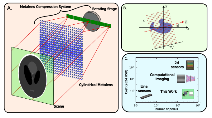
A visual diagram of the Radon transform is shown in Figure 1B. This integral can be interpreted as taking the average value of the function along the line of integration. Serendipitously, when imaging a scene at the back focal plane of a cylindrical lens, this functionality is achieved when recording the pixel values along the focal line of the lens as shown in Figure 1A. Thus the Radon transform can be implemented optically by using a cylindrical lens and a line detector, and rotating the system to record the line-average of the scene at different angles. We note that due to the use of a line detector, our system provides a promising alternative to expensive, high pixel density 2D optical sensors, as shown in Figure 1C.
To optically implement the Radon transform, we designed a metalens with a cylindrical phase profile, operating at wavelength. The phase profile is given as:
| (3) |
In the above equation, and are the spatial coordinates of the metalens and is the focal length of the metalens. Note that, since this is a cylindrical metalens, the phase profile only varies in one direction, chosen to be in our case. We used crystalline Silicon on Sapphire substrate as the material platform for the metalens. The scatterer geometry used in this work is square pillars with height , at periodicity of . We computed the amplitude and phase response of the scatterers using Rigorous Coupled Wave Analysis (RCWA). The constructed electromagnetic response vs scatterer geometry library is shown in LABEL:fig:s1. Due to the manufacturing constraints, we constrained the pillar diameters to vary between and . To design the meta-optic, we first discretized the phase profile in equation 3 by the pillar periodicity on a 2 dimensional grid. At every point , we matched the computed lens phase profile to the pillar with the closest phase response:
| (4) |
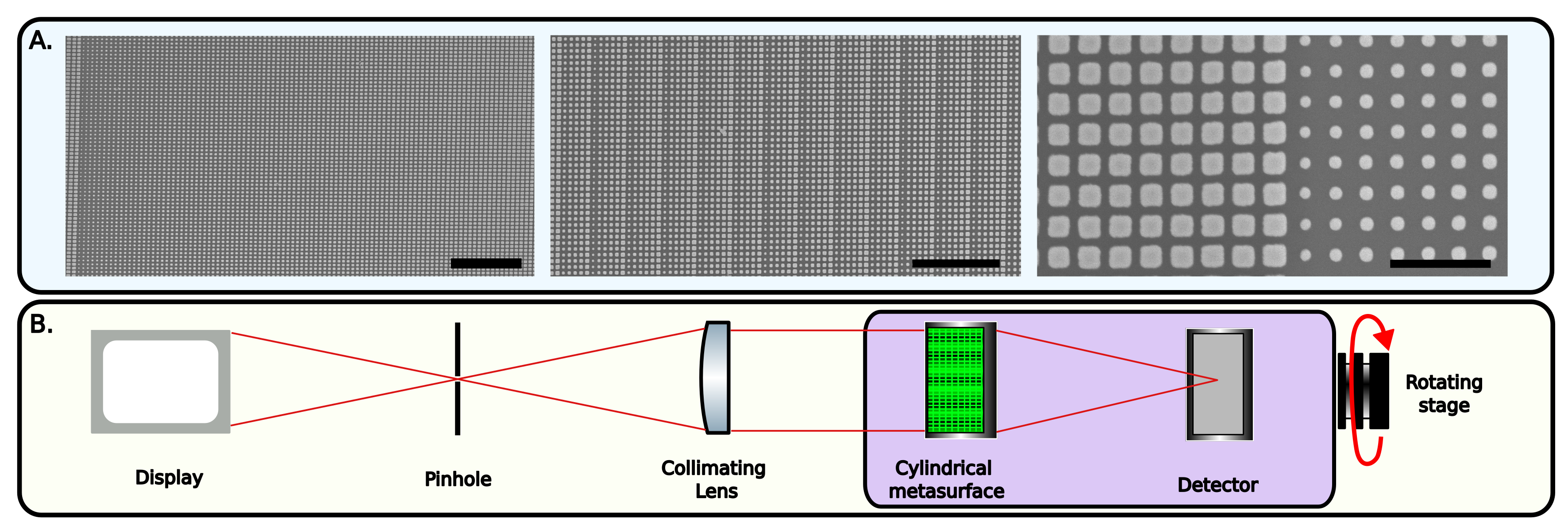
The pillar distribution of the meta-optic is shown in LABEL:fig:s1-. Scanning electron micrographs of the manufactured device are shown in Figure 2 A. To carry out the experiment, we mounted the metalens, and a detector onto a rotating stage. In order to image the DC component of the Fourier transform of an image, we placed a pinhole and a collimating lens in front of the meta-optic, and used an electronic display to image different scenes with the system. Figure 2 B. shows the schematic of the optical setup.
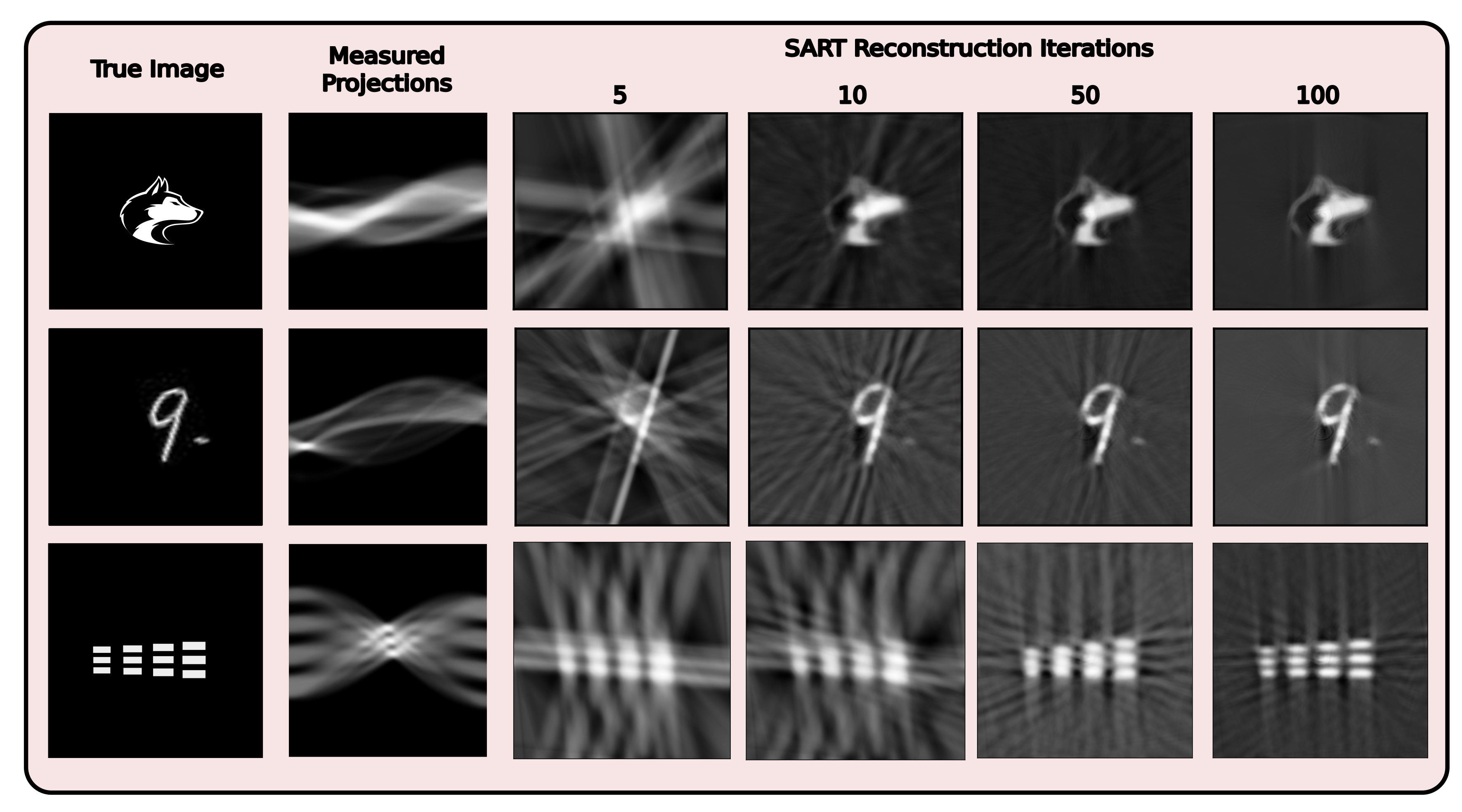
The measurement was carried out by recording the line pixel data along different angular positions at the back focal plane of the cylindrical meta-optic. For measurement we used a regular pixel detector, while only pixel values along the focal line were stored to emulate a line detector. In experiment, we stored different line projections corresponding to rotations between and . To reconstruct the image we used the Simultaneous Algebraic Reconstruction Technique (SART) (?, ?, ?), which is a commonly used iterative reconstruction technique in medical imaging. Figure 3 shows 3 examples of measured Radon transforms and the reconstructed results using this technique, a picture of a husky, an MNIST number 9, and a horizontal resolution line target. We observe that the reconstruction converges after about 100 iterations, with no significant improvemenet with subsequent iterations. Note that since we only measure pixels in the Radon domain, which corresponds to a compression ratio in the reconstructed pixel image. Because the scenes we measured in this work are relatively dense (a single image essentially occupies most pixels) and lack many features, a simple average pooling filter which can be implemented by binning groups of nearby pixels achieves a similar imaging performance. Nevertheless, it is theoretically possible to achieve a better imaging performance on sparsely featured scenes (like a digit with a wide background) while capturing fewer pixels than in the original scene. For more details see LABEL:s3 and LABEL:fig:s3.
Neural network classification in Radon Space
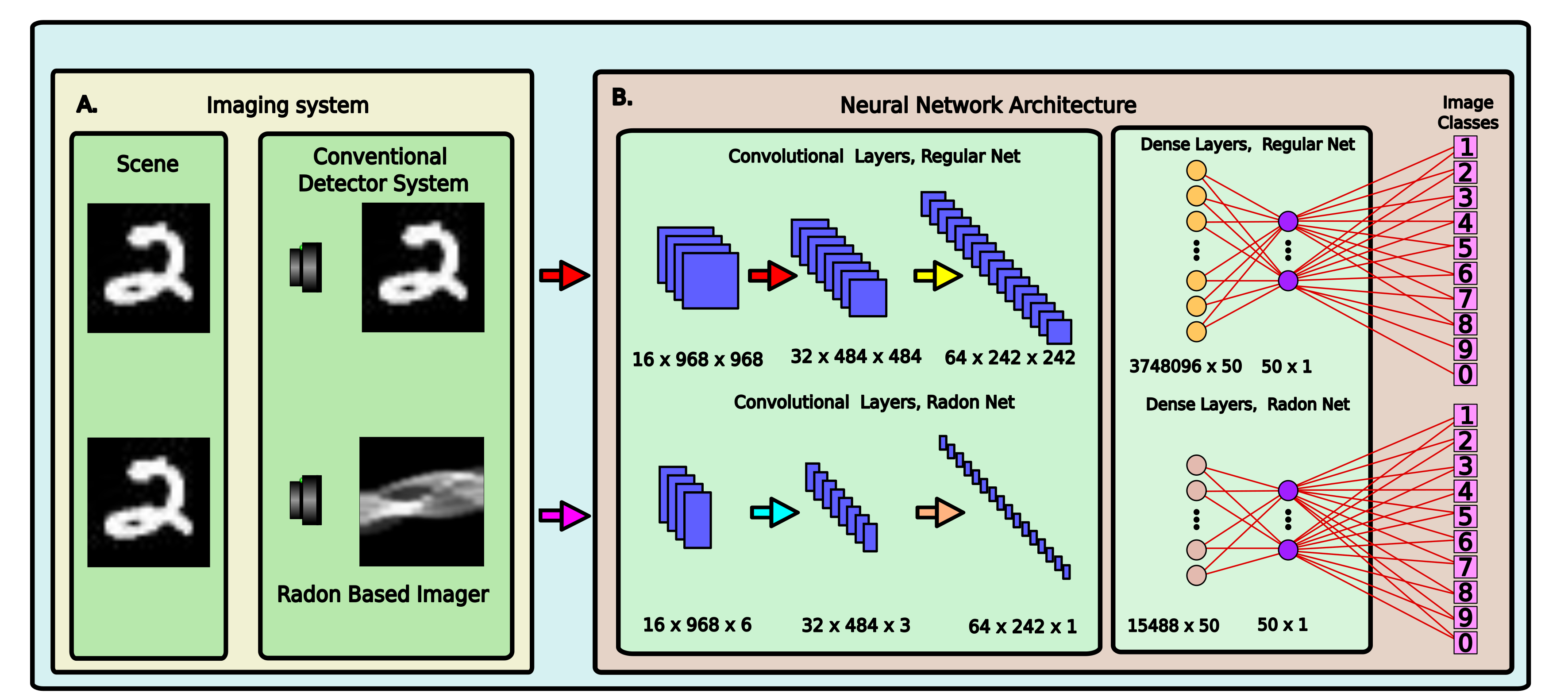
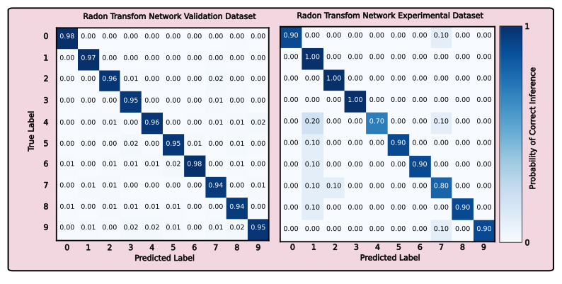
While reconstruction is often used to create an aesthetically pleasing image, for many machine vision problems, such as classification, we can directly utilize the captured data. By using a neural network-based back end, we can classify images in the radon space. For this task, we selected a common neural network architecture used in classification tasks called AlexNet (?) consisting of convolutions, max pool layers, and dense layers. We used a modified version of AlexNet, with 3 convolutional layers and 2 dense layers. The neural network architecture is shown in Figure 4. To train the network we used the MNIST dataset. The MNIST data set consists of pixel images of numbers 0-9. To train the network, we first padded the images by 14 pixels on each side to resemble the scale of the raw data captured in the experiment. Then, since our imaging setup uses a pixel detector, we rescaled our images to fit this dimensionality. In order to correct for experimental rotation and misalignment, we performed random affine transforms of the real space images with rotations varying between , translations between of the image width, and scaling between of the image size. To incorporate noise in our model, we added Gaussian noise to the raw images. Before feeding the images into the neural network, we radon transformed the images, keeping 23 angular projections in the sinogram evenly space between and . After training, we achieved a classification accuracy on the validation set. To test the network with experimental data, we collected 100 experimental images of the MNIST data set (such as the number shown in Figure 3) with the same angular spacing in the radon domain. Each classification class had 10 images. Classifying our experimental dataset, we achieved a classification accuracy of . Figure 5 shows the confusion matrices of the radon transform neural networks. We emphasize that, the network is not retrained with the experimental data, and training a network with only synthetic data generally yields much lower accuracy.
Discussion
In this paper, we presented and experimentally validated a meta-optical imaging system based on the Radon transform. The system is composed of a cylindrical metalens, a rotating stage, and a line detector which measured Radon projections of an image at different angles. The proposed system provides a key advancement in optical realizations of mathematical transforms with applications in accelerating image processing. We achieve imaging of a real scene, by capturing of the reconstructed image’s pixels, effectively compressing the scene in the optical domain. The proposed system also offers a few advantages over conventional imaging systems. Firstly, line sensors with a large number of pixels in the order of are readily commercially available. This offers a unique advantage for the proposed imaging system over conventional 2D detector, which will be particularly well-suited for longer wavelengths, inclusing mid/ long wave infrared. By measuring projections of pixels per angle, an pixel imaging system can be built without using pixels, offering significant cost and power reduction, enabling megapixel systems to be built efficiently.
The current setup is in fact a prototype and could be improved upon. It takes approximately 5-6 minutes to collect 180 Radon slices in order to reconstruct the full image. This is due to the long exposure time ( seconds) needed to capture an image due to the inclusion of a pinhole. Furthermore, the rotating stage adds a moving part to the system which is less than ideal for realistic imaging setups. Nevertheless, both of these issues can be avoided by manufacturing a two layer meta-lenslet array. One of the meta-lenslet array would have cylindrical phase profiles oriented at different angles. The other would have regular hyperboloid profiles effectively serving as the collimating lenses. Then we would use linear detectors at the focal plane of the system to collect the Radon transform in a single shot.
Another key aspect of this work shows the classification of images in a transformed domain. To the best of the authors’ knowledge, most current works that use transformation optics as a front-end to a neural network, require both a simulated dataset, as well as experimental data that use those optics for calibration. This of course adds complexity to a system, and often even requires a digital calibration layer. In this work we demonstrate that experimental calibration is not strictly required if you carefully design a transformation optic based on mathematically known transforms that can easily be simulated on a computer.
Fabrication Methods
We used commercially available silicon on sapphire wafers with a film thickness of 500 nm from University Wafer. Wafer were diced into square chips with a side length of 2 cm. After thorough cleaning in an ultrasound bath of Acetone and subsequently IPA, we dry-cleaned the chips and used a further barrel etching step to remove organic residues. We then spin coated a positive resist (ZEP 520-A) onto the sample, with a subsequent baking step on a hot plate. To mitigate charging issues, a conductive polymer layer was further spun onto the substrate (DisCharge H2O). We then patterned the design into the resist using a 100 keV electron beam (JEOL JBX6300FS) at a dose of 275 muC cm-2. The conductive polymer layer was then removed in IPA and the chip was then developed using Amyl Acetate. Subsequently, we appplied another barrel etch step to remove remaining residues. After development, we deposited a layer of 50 nm alumina using an e-beam evaporator and subsequent lift off in NMP. After further cleaning, the silicon was etchined in a dry etcher using a mixture of C4F8/SF6.
Measurement Methods
The cylindrical metalens was mounted one focal length in front of a sensor (ASI174MM) with a narrow band pass filter on a rotating mount. This imager was placed at the focal plane of a 4f system, consisting of an OLED display, a lens with 200 mm focal length, a pinhole with a diameter of 200 micron, and a second lens with a focal length of 50 mm. Thus the 4f system enabled a spatially coherent input for the radon imager, while also demagnifying the image by a factor of 4. All measurements were automated using custom written python scripts.
References and Notes
- 1. J. Goodman, Introduction to Fourier Optics, McGraw-Hill physical and quantum electronics series (W. H. Freeman, 2005).
- 2. Z.-H. Gu, J. R. Leger, S. H. Lee, Optics Communications 39, 137 (1981).
- 3. K. W. W. K. W. Wong, L. M. C. L. M. Cheng, Japanese Journal of Applied Physics 31, 1672 (1992).
- 4. M. R. Mueller, F. P. Carlson, Appl. Opt. 14, 2207 (1975).
- 5. G. Shabtay, D. Mendlovic, Z. Zalevsky, Appl. Opt. 37, 2964 (1998).
- 6. T. Ilovitsh, A. Ilovitsh, J. Sheridan, Z. Zalevsky, Opt. Express 22, 32301 (2014).
- 7. A. Zhan, et al., ACS Photonics 3, 209 (2016).
- 8. S. Wang, et al., Nature Nanotechnology 13, 227 (2018).
- 9. A. Zhan, S. Colburn, C. M. Dodson, A. Majumdar, Scientific Reports 7, 1673 (2017).
- 10. S. Colburn, A. Zhan, A. Majumdar, Optica 5, 825 (2018).
- 11. R. Audhkhasi, J. E. Fröch, A. Zhan, S. Colburn, A. Majumdar, Applied Physics Letters 123, 150502 (2023).
- 12. S. Colburn, A. Zhan, A. Majumdar, Science Advances 4, eaar2114 (2018).
- 13. E. Tseng, et al., Nature Communications 12, 6493 (2021).
- 14. J. E. Fröch, et al., Beating bandwidth limits for large aperture broadband nano-optics (2024).
- 15. Y. Dong, et al., ACS Photonics 11, 1645 (2024).
- 16. R. Maman, E. Mualem, N. Mazurski, J. Engelberg, U. Levy, ACS Photonics 10, 4494 (2023).
- 17. J. E. Fröch, et al., ACS Photonics 10, 986 (2023).
- 18. S. Colburn, A. Majumdar, ACS Photonics 7, 1529 (2020).
- 19. F. Yang, H.-I. Lin, P. Chen, J. Hu, T. Gu, Nanophotonics 12, 2987 (2023).
- 20. Q. Guo, et al., Proc Natl Acad Sci U S A 116, 22959 (2019).
- 21. Z. Shen, et al., Nature Communications 14, 1035 (2023).
- 22. H. Zheng, et al., Science Advances 8, eabo6410 (2022).
- 23. L. Huang, et al., Nanophotonics 13, 1191 (2024).
- 24. H. Zheng, et al., Nature Nanotechnology 19, 471 (2024).
- 25. A. Wirth-Singh, et al., Compressed meta-optical encoder for image classification (2024).
- 26. K. Wei, et al., Spatially varying nanophotonic neural networks (2023).
- 27. T. Fu, et al., Light: Science & Applications 13, 263 (2024).
- 28. X. Lin, et al., Science 361, 1004 (2018).
- 29. A. Wirth-Singh, et al., CLEO 2024 (Optica Publishing Group, 2024), p. FF1J.1.
- 30. Z. Fang, et al., ACS Nano 18, 11245 (2024).
- 31. J. Park, et al., Nat. Nanotechnol. 16, 69 (2021).
- 32. G. K. Shirmanesh, R. Sokhoyan, P. C. Wu, H. A. Atwater, ACS Nano 14, 6912 (2020).
- 33. P. Moitra, et al., ACS Nano 17, 16952 (2023).
- 34. R. Chen, et al., Opt. Mater. Express 13, 2416 (2023).
- 35. B. Bai, et al., Light: Science & Applications 12, 69 (2023).
- 36. X. Gao, et al., IEEE Photonics Journal 13, 1 (2021).
- 37. A. S. Ostrovsky, E. P. Mota, J. I. Cuatianquiz, Optics and Lasers in Engineering 40, 43 (2003). Optics in Latin America part II.
- 38. J. Hanawa, T. Niiyama, Y. Endo, S. Sunada, Opt. Express 30, 22911 (2022).
- 39. J. Radon, Berichte über die Verhandlungen der Sächsische Akademie der Wissenschaften 69, 262 (1917). 00000.
- 40. A. M. Cormack, Journal of Applied Physics 34, 2722 (1963).
- 41. W. van Aarle, et al., Optics Express 24, 25129 (2016).
- 42. W. van Aarle, et al., Ultramicroscopy 157, 35–47 (2015).
- 43. W. Palenstijn, K. Batenburg, J. Sijbers, Journal of Structural Biology 176, 250–253 (2011).
- 44. A. Krizhevsky, I. Sutskever, G. E. Hinton, Advances in Neural Information Processing Systems, F. Pereira, C. Burges, L. Bottou, K. Weinberger, eds. (Curran Associates, Inc., 2012), vol. 25.