Aharonov-Bohm interferometer in inverted-band pn junctions
Abstract
Inverted-band junctions in two-dimensional materials offer a promising platform for electron optics in condensed matter, as they allow to manipulate and guide electron beams without the need for spatial confinement. In this work, we propose the realization of an Aharonov-Bohm (AB) interferometer using such junctions. We observe AB oscillations in numerically obtained conductance and analytically identify the conditions for their appearance by analyzing the scattering processes at the interface. To support experimental implementation, we also consider junctions with a graded interface, where the potential varies smoothly between the - and -doped regions. Our results reveal an abrupt change in the AB-oscillation frequency, which we attribute to a distinct transition in the hybridization across the interface. We verify that our reported AB oscillations are robust to realistic disorder and temperature decoherence channels. Our study paves the way for realizing the Aharonov-Bohm effect in bulk mesoscopic systems without the need for external spatial confinement, offering new possibilities in electron optics.
The Aharonov-Bohm (AB) effect is one of the cornerstone phenomena highlighting the non-local nature of quantum mechanics [1, 2, 3]. The effect arises when two quantum trajectories enclose a finite magnetic flux, making their interference dependent on the external magnetic field [4]. On a microscopic scale, the AB effect has been observed in a wide range of systems, and plays a pivotal role in revealing quantum phenomena in transport that strongly depends on magnetic fields, e.g. in revealing weak localization through magnetoresistance measurements [5, 6].
To directly realize an AB interferometer in a mesoscopic system, a variety of two-dimensional platforms have been employed [7, 8, 9, 10, 11, 12, 13, 14], where clear oscillations in transport as a function of an external magnetic field were observed. The primary challenges in observing such AB oscillations lie in the ability to prepare well-defined electron paths while maintaining coherence between electrons traveling along them [7, 15]. Guiding electrons in such a manner is inherently difficult and has traditionally been achieved through spatial confinement using etching techniques [9, 13], gating [16, 11], or by employing strong magnetic fields to confine electrons along the one-dimensional edges of a quantum Hall droplet [17, 18, 19, 20, 21, 14].
Recently [22], we proposed a protocol for directing electrons using inverted-band -junctions, without relying on external spatial confinement of the electron trajectories. Such junctions filter the electronic trajectories via a Klein tunneling-alike effect, allowing passage based on the incident angle at the interface [22]. Unlike Klein tunneling in Dirac materials [23], the filtering occurs at finite incident angles that are readily controlled by tuning the chemical potential of the junction. Crucially to this work, a narrow window of negative refraction scattering processes – involving both particle-like and hole-like Fermi surfaces – manifests and generates interfering closed paths for the electron trajectories.
In this work, we propose how to realize an Aharonov-Bohm interferometer using a two-dimensional inverted-band junction. The AB effect in our setup arises from two key ingredients: (i) negative refraction between distinct Fermi surfaces in the - and -doped regions, which creates closed loops of different electronic trajectories between point-like source and drain leads, and (ii) angular filtering of trajectories at the interface, resulting in a limited number of trajectories that coherently interfere upon reaching the drain lead. In the presence of a weak perpendicular magnetic field, we predict that clear AB oscillations appear due to nonlocal interference. We numerically demonstrate the effect for a realistic experimental setting by adapting the band structure of InAs/GaAs [24]. We further show that these oscillations persist even in the situation when the interface has a finite length. Interestingly, we find that the frequency of the AB oscillations changes abruptly beyond a certain interface length, which we attribute to a shift in the maximal transmission angle due to a transition of the interface to an opaque barrier. Our work brings magnetic control to electron optics applications in two-dimensional mesoscopic devices.
Model — To model the inverted band junction (see Fig. 1), we consider the following 2D spinless Hamiltonian [24, 22],
| (1) |
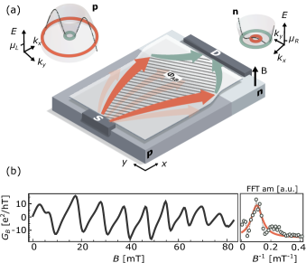
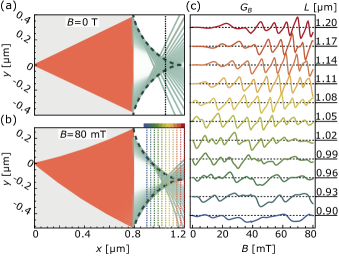
where are Pauli matrices acting on two bands, and denotes a 2D wavevector. The bare, uncoupled energy dispersions are particle- and hole-like in nature with respective effective masses , where we assume . Particle-hole symmetry is maintained for . Such bare energy dispersions overlap with magnitude and hybridize with coupling strength . The local chemical potential , experimentally tunable by backgates [24], takes different values in the -doped and -doped regions. We assume these regions to respectively reside on the left- and right-hand sides of the interface, i.e., and . Diagonalizing the Hamiltonian (1) yields the two dispersions . In the inverted-band regime, when , the resulting band structure resembles two sombreros facing one another, and separated by a gap, see Fig. 1(a). We label the spinor eigenstates of (1) as , where refers to the left- and right-hand side of the junction and indicates the particle or hole-like Fermi surface, cf. Fig. 1(a). The superscript denotes the direction of group velocity relative to the interface. In the following, we consider the junction when the chemical potentials, , lie within the band-overlap energy interval of each sombrero. Specifically, we are interested in the response of the junction to an external perpendicular magnetic field, .
Sharp interface setup— To numerically probe the transport properties of the system (1), we incorporate the aforementioned junction into the numerical toolbox Kwant [25]. To simulate a realistic transport experiment, we draw the junction along the -direction, and include two metallic leads on the junction’s ends. These source (S) and drain (D) leads are positions on the left and right sides, respectively, and have finite widths in the -direction, which are much shorter than the sample size, see Fig. 1(a). The spatial distance between the junction interface and the leads is chosen carefully, such that injected hole-like states from S maximally refocus in D as particle-like states [26]. Similarly, the spatial extent of the junction in the -direction is chosen such that the refocusing scattering states will not hit the boundaries. To remove background noise from finite-size effects, we attach additional absorbing leads along the top and bottom boundaries. The system’s dimensions we use are taken relative to realistic Fermi wavelengths of InAs/GASb inverted-band semiconductors [24, 26]. The perpendicular magnetic field is introduced using standard Peierls substitution [27]. We then study the two-terminal conductance between the leads by numerically evaluating the Landauer-Buttiker formula [28]
| (2) |
where is the transmission coefficient from the -th mode in the source lead to the -th mode in the drain lead. The total numbers of modes and in the leads are determined by the widths of the leads.
Main result— In Fig. 1(b), we plot the resulting two-terminal conductance for magnetic fields ranging between mT. We find that the magneto-differential conductance exhibits clear periodic oscillations with an average period . As we show below, such oscillations in arise due to a mesoscopic AB effect whose origin lies in negative refraction at the interface. This is the main result of our work. We emphasize that such an emergence of AB oscillations in a simple 2D junction that does not rely on any external spatial confinement is surprising [4].
To explain the mechanism of the oscillations in our system, we first notice that, in our regime of weak magnetic fields, the trajectories of the propagating states are only weakly affected by the magnetic field, i.e., they remain describable by “ray tracing” that emanate from the source in the - and -doped regions, separately [26]. Hence, in this limit, AB oscillations can emerge only when the following two prerequisites are satisfied: (i) the interface between the - and -doped region facilitates negative refraction that refocuses the trajectories at the drain lead where they interfere, and (ii) only a narrow distribution of incident angles participates in the negative refraction, such that the interference pattern survives decoherence via averaging over the contributions of many incident trajectories that carry different phases. Shown below, the latter will be the result of filtering by the transmission coefficients at the interface.
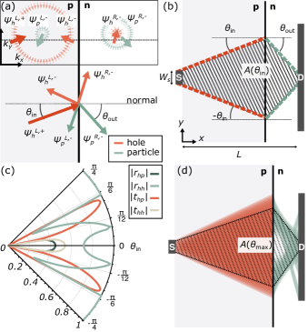
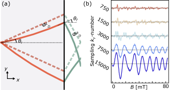
To demonstrate (i), we consider an incident hole-like spinor from the source with momentum , see Fig. 2(a). We assume that the junction is homogeneous along the -direction, such that is conserved in all scattering processes. Thus, we can determine the outgoing states and their corresponding momenta from momentum conservation at the Fermi surface, cf. band structures in insets of Fig. 2(a), and Ref. [22]. Note that the incident and outgoing states are defined with respect to the interface, as illustrated in Fig. 2(a). The propagating direction of each scattering state is given by its group velocity , see arrows in upper panel of Fig. 2(a). Crucially, the hole-to-particle transmission scattering process exhibits negative refraction at the interface, i.e., for with a positive incident angle , the outgoing particle-like spinor in the -doped region propagates at a negative angle . This trajectory can interfere at the drain lead with another trajectory where impinges on the interface at , see Fig. 2(b). Crucially, the two interfering paths encircle a kite-shaped area
| (3) |
where is the distance between S and D. The value of represents the ratio between the length of the - and -doped region, which is chosen according to the focal point of trajectories [26], see also Fig. 2(b). Finally, accounts for the added area introduced by the finite width of the source lead.
To check if (ii) is satisfied, we employ a scattering matrix formalism [26] to calculate the transmission , and reflection and scattering coefficients as a function of the incident angle, , where we assume an incident hole-like spinor (first subscript = ) and consider all four possible outgoing cases, see Fig. 2(c). At most angles the dominant process is a reflection of a hole, , making the junction very opaque. Interestingly, we find that , which leads to negative refraction, maximizes in a narrow range around a finite incident angle [26]. In other words, electrons transmitted through the junction are mostly carried by trajectories incident around , while the other angles are screened by the interface. We demonstrate this effect by drawing the ray trajectories of the hole-like states injected from the source and transmitted as particle-like states into the drain lead, see Fig. 2(d). The drawn trajectories’ opacity is taken according to their transmission amplitude at the interface, cf. Fig. 2(c). Thus, we find a large depleted area due to the transmission filtering at small angles and high density only in a narrow scattering angle region. Note that by taking only the two trajectories with the maximal into account, defined by and marked by dashed lines in Fig. 2(d), we can use Eq. (3) to obtain for and in our setup.
Each scattering trajectory follows a path and accumulates a dynamical phase . To these paths, we can introduce the perpendicular magnetic field as a vector potential , where it may impact the scattering amplitudes in three ways: (i) bend the trajectories due to a Lorentz force, (ii) alter the scattering angles and amplitudes at the junction, and (iii) introduce an Aharonov-Bohm (AB) phase to the interfering paths via minimal coupling, . Neglecting (i) and (ii) due to the weak magnetic fields we used, we can divide the sum in Eq. (2) into terms that do not include interfering paths (where the accumulated phase is irrelevant) and interfering scattering trajectories that are impacted by the magnetic flux through the area A. We can, moreover, assume that the dominant magnetic-field dependent scattering process involves the paths at [26], leading to
| (4) |
where is the flux threading the enclosed area . The magnetic response (4), therefore, exhibits a period that is solely determined by the AB phase. In our case, we obtain a period of mT, which is in good agreement with the one extracted from the numerics, cf. Fig. 1(b).
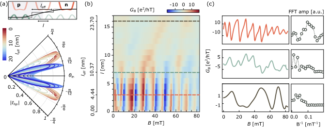
Graded interface— Perfectly sharp interfaces cannot be realized in experiments. We, therefore, proceed to check how the predicted AB oscillations behave in the presence of a graded interface. We model it by introducing a spatially modulated chemical potential , where is its characteristic length, see in Fig. 3(a). Importantly, this interpolation introduces an effective gapped region between the and regions. We numerically calculate as a function of and show it in Fig. 3(b). We observe a clear change in the oscillating pattern at . More quantitatively, the frequency of oscillation in reduces for smoother interfaces, cf. three cuts at , , and in Fig. 3(c).
To gain a deeper understanding of the observations discussed above, we analytically describe an effective potential barrier induced by the smooth interface by employing an effective two-interface model. As the Fermi level leaves the upper/lower band at energies , the barrier between the - and -doped regions has an effective length with . In this simplified model, we assume the interfaces between the three regions to be sharp; see the dashed line in the upper panel of Fig. 3(a). Using the S-matrix formalism, we once more calculate the transmission amplitude as a function of the incident angle and effective barrier length [26] and show the result in the lower panel of Fig. 3(a). For a short barrier , we obtain a similar behavior as in the previous case of a vanishing barrier, with negative refraction centered around . Interestingly, with increasing , we find a crossover in the behavior of , i.e., the maximal transmitted angle undergoes an abrupt transition at . As a result, for a longer interface , maximizes at a smaller angle of , which implies a smaller enclosed area , and a different AB-oscillation period that follows from Eq. (4), which is in agreement with the numerical results, cf. Fig. 3. We attribute this transition to a competition between the length of the barrier and the decay length of evanescent waves penetrating the barrier from the interfaces [29]: the system enters the tunneling limit when the electrons only tunnel through the overlapping evanescent tails, resulting in an abrupt change of the [26].
In conclusion, we propose the realization of an AB-interferometer using negative refraction in a two-dimensional inverted-band junction. A key difference, compared with common AB interferometers, is that we do not impose external spatial confinement on the trajectories of electrons; instead, the confinement emerges naturally due to the band structure’s characteristic sombrero shape. Specifically, using the S-matrix formalism, we find that the negative refraction transmission amplitudes are facilitated by hole-to-particle scattering , whose distribution maximizes in a narrow range of incident angles. The latter realizes an effective spatial confinement that guides electrons [22]. This emergent spatial confinement entails that all transmitted electronic trajectories exhibit a kite-shaped enclosed surface which, under the external magnetic field, gives rise to unique AB oscillations in conductance. Commonly, one would expect a reduction in the transmission due to a smooth interface [23], while, on the contrary, we find that the oscillations persist with a distinct change in the AB-oscillation period. Moreover, we tested the robustness of the AB oscillations against finite temperature and disorder [26]. We observe clear oscillations up to temperatures of and disorder strength of several meV-s, which gives strong indications that the proposed setup can be realized in realistic experimental situations. The proposed mechanism of generating AB interference is related to the sombrero hat shape of the band structure, which can be found in a plethora of systems; including -wave and chiral -type superconductors [30], heterostructures with strong Rashba spin-orbit interaction like HgTe/CdTe [31] and InAs/GaSb [24], two-dimensional monochalcogenides like GaSe [32] and transition metal dichalcogenides like WTe2 [33]. Moreover, the Bernal bilayer graphene, which is known for its tunability of the sombrero-hat bandstructure under a biased voltage [34, 35, 36], suggests potential realizations of AB interferometer with graphene-based material. With all of the aforementioned, we think that the physics discussed in this work can be experimentally tested in current state-of-the-art mesoscopic platforms.
acknowledgments
This work was supported by the Deutsche Forschungsgemeinschaft (DFG) through project number 449653034, and ETH research grant ETH-28 23-1. The work of A.Š. is supported by the European Union’s Horizon Europe research and innovation programme under the Marie Skłodowska-Curie Actions Grant agreement No. 101104378.
References
- Ehrenberg and Siday [1949] W. Ehrenberg and R. E. Siday, Proceedings of the Physical Society. Section B 62, 8 (1949).
- Aharonov and Bohm [1959] Y. Aharonov and D. Bohm, Physical Review 115, 485 (1959).
- Aharonov and Bohm [1961] Y. Aharonov and D. Bohm, Physical Review 123, 1511 (1961).
- [4] T. Ihn, Semiconductor Nanostructures: Quantum States and Transport, (Oxford University Press, 2009).
- [5] E. Akkermans and G. Montambaux, Mesoscopic Physics of Electrons and Photons, (Cambridge University Press, 2007).
- Chen et al. [2019] W. Chen, H.-Z. Lu, and O. Zilberberg, Physical Review Letters 122, 196603 (2019).
- van Oudenaarden et al. [1998] A. van Oudenaarden, M. H. Devoret, Y. V. Nazarov, and J. E. Mooij, Nature 391, 768 (1998).
- Bachtold et al. [1999] A. Bachtold, C. Strunk, J.-P. Salvetat, J.-M. Bonard, L. Forró, T. Nussbaumer, and C. Schönenberger, Nature 397, 673 (1999).
- Russo et al. [2008] S. Russo, J. B. Oostinga, D. Wehenkel, H. B. Heersche, S. S. Sobhani, L. M. K. Vandersypen, and A. F. Morpurgo, Physical Review B 77, 085413 (2008).
- Kremer et al. [2020] M. Kremer, I. Petrides, E. Meyer, M. Heinrich, O. Zilberberg, and A. Szameit, Nature Communications 11, 907 (2020).
- Iwakiri et al. [2024] S. Iwakiri, A. Mestre-Torà, E. Portolés, M. Visscher, M. Perego, G. Zheng, T. Taniguchi, K. Watanabe, M. Sigrist, T. Ihn, and K. Ensslin, Nature Communications 15, 390 (2024).
- Kawaguchi et al. [2024] Y. Kawaguchi, D. Smirnova, F. Komissarenko, S. Kiriushechkina, A. Vakulenko, M. Li, A. Alù, and A. B. Khanikaev, Science Advances 10, eadn6095 (2024).
- Kim et al. [2024] J. Kim, H. Dev, R. Kumar, A. Ilin, A. Haug, V. Bhardwaj, C. Hong, K. Watanabe, T. Taniguchi, A. Stern, and Y. Ronen, Nature Nanotechnology , 1 (2024).
- Biswas et al. [2024] S. Biswas, H. K. Kundu, R. Bhattacharyya, V. Umansky, and M. Heiblum, Physical Review Letters 132, 076301 (2024).
- Zilberberg et al. [2011] O. Zilberberg, A. Romito, and Y. Gefen, Phys. Rev. Lett. 106, 080405 (2011).
- Iwakiri et al. [2022] S. Iwakiri, F. K. De Vries, E. Portolés, G. Zheng, T. Taniguchi, K. Watanabe, T. Ihn, and K. Ensslin, Nano Letters 22, 6292 (2022).
- Klitzing et al. [1980] K. v. Klitzing, G. Dorda, and M. Pepper, Physical Review Letters 45, 494 (1980).
- Özyilmaz et al. [2007] B. Özyilmaz, P. Jarillo-Herrero, D. Efetov, D. A. Abanin, L. S. Levitov, and P. Kim, Physical Review Letters 99, 166804 (2007).
- Amet et al. [2014] F. Amet, J. Williams, K. Watanabe, T. Taniguchi, and D. Goldhaber-Gordon, Physical Review Letters 112, 196601 (2014).
- Nichele et al. [2016] F. Nichele, H. J. Suominen, M. Kjaergaard, C. M. Marcus, E. Sajadi, J. A. Folk, F. Qu, A. J. A. Beukman, F. K. d. Vries, J. v. Veen, S. Nadj-Perge, L. P. Kouwenhoven, B.-M. Nguyen, A. A. Kiselev, W. Yi, M. Sokolich, M. J. Manfra, E. M. Spanton, and K. A. Moler, New Journal of Physics 18, 083005 (2016).
- Nguyen et al. [2016] B.-M. Nguyen, A. A. Kiselev, R. Noah, W. Yi, F. Qu, A. J. Beukman, F. K. de Vries, J. van Veen, S. Nadj-Perge, L. P. Kouwenhoven, M. Kjaergaard, H. J. Suominen, F. Nichele, C. M. Marcus, M. J. Manfra, and M. Sokolich, Physical Review Letters 117, 077701 (2016).
- Zhao et al. [2023] Y. Zhao, A. Leuch, O. Zilberberg, and A. Štrkalj, Physical Review B 108, 195301 (2023).
- Cheianov and Fal’ko [2006] V. V. Cheianov and V. I. Fal’ko, Physical Review B 74, 041403 (2006).
- Karalic et al. [2020] M. Karalic, A. Štrkalj, M. Masseroni, W. Chen, C. Mittag, T. Tschirky, W. Wegscheider, T. Ihn, K. Ensslin, and O. Zilberberg, Physical Review X 10, 031007 (2020).
- Groth et al. [2014] C. W. Groth, M. Wimmer, A. R. Akhmerov, and X. Waintal, New Journal of Physics 16, 063065 (2014).
- [26] See Supplemental Material at URL-will-be-inserted-by-publisher for the detailed explanation.
- Peierls [1933] R. Peierls, Zeitschrift für Physik 80, 763 (1933).
- Büttiker [1988] M. Büttiker, Physical Review B 38, 9375 (1988).
- Yao et al. [2024] J. Yao, B. Zhou, X. Zhou, X. Xiao, and G. Zhou, Anomalous quantum scattering and transport of electrons with Mexican-hat dispersion induced by electrical potential (2024), arXiv:2403.09319 [cond-mat].
- Štrkalj et al. [2024] A. Štrkalj, X.-R. Chen, W. Chen, D. Y. Xing, and O. Zilberberg, Physical Review Letters 132, 066301 (2024).
- Minkov et al. [2013] G. M. Minkov, A. V. Germanenko, O. E. Rut, A. A. Sherstobitov, S. A. Dvoretski, and N. N. Mikhailov, Physical Review B 88, 155306 (2013).
- Li et al. [2014] X. Li, M.-W. Lin, A. A. Puretzky, J. C. Idrobo, C. Ma, M. Chi, M. Yoon, C. M. Rouleau, I. I. Kravchenko, D. B. Geohegan, and K. Xiao, Scientific Reports 4, 5497 (2014).
- Qian et al. [2014] X. Qian, J. Liu, L. Fu, and J. Li, Science 346, 1344 (2014).
- Min et al. [2007] H. Min, B. Sahu, S. K. Banerjee, and A. H. MacDonald, Physical Review B 75, 155115 (2007).
- Castro et al. [2007] E. V. Castro, K. S. Novoselov, S. V. Morozov, N. M. R. Peres, J. M. B. L. Dos Santos, J. Nilsson, F. Guinea, A. K. Geim, and A. H. C. Neto, Physical Review Letters 99, 216802 (2007).
- McCann et al. [2007] E. McCann, D. S. Abergel, and V. I. Fal’ko, The European Physical Journal Special Topics 148, 91 (2007).
Supplemental Material: Aharonov-Bohm interferometer in inverted-band pn junctions
S1 Details on the numerical simulation using Kwant
Throughout the paper, unless specified otherwise, we use the following parameters: , , and , which approximate the bandstructure of InAs/GaAs [24] [cf. Eq. (1) in the main text]. To numerically calculate the transport through the system described in the main text, we first discretize the continuous Hamiltonian and define a tight-binding Hamiltonian over a finite-size region containing sites in the -direction (length) and sites in the -direction (width). The length of the - and -doped region is and , respectively. We set the lattice spacing to , such that for the aforementioned values of parameters, the smallest Fermi wavelength is about 15 times larger than the lattice spacing. This ensures that our lattice model reliably describes the continuum system at the given low energies energies that we use.
We attach semi-infinite leads on each side of the junction, where the source lead width is sites and the drain lead width is sites. We assume that both leads are normal metals with parabolic dispersions, i.e., we adopt the Hamiltonian from Eq. (1) and set , and for that purpose. With the setup defined, we use Kwant [25] to obtain the non-local conductance between the source and the drain lead, corresponding to Eq. (2) in the main text.
S2 Conductance at finite temperatures and in the presence of disorder
In this section, we study the performance of the AB interferometer at finite temperatures and its robustness against disorder. First, to study the influence of finite temperatures: we calculate the temperature-dependent conductance as
| (S1) |
where is the Boltzmann constant and is conductance defined in Eq. (2) in the main text at energy . We repeat the simulation times for different sampled out of the distribution , such that the integral above is evaluated using a Riemann sum.
We show the results in Fig. S1(a), where in order to emphasize the oscillations, we plot as a function of . The amplitude of the oscillation decreases with increasing temperature and vanishes when the temperature approaches . Nevertheless, for , the oscillation pattern is clearly visible, meaning that it should be possible to observe it in a realistic experimental situation.
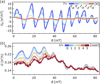
Similarly, we find that the oscillation pattern persists also when introducing moderate disorder. For the latter, we introduce a random onsite potential sampled out of a normal distribution with zero mean and the standard deviation . As shown in Fig. S1(b), the disorder introduces random fluctuations into the conductance . Nonetheless, the oscillation pattern remains recognizable up to , which corresponds to a thermal fluctuation at .
S3 Scattering matrix formalism
We employ a scattering matrix (S-matrix) formalism [24, 22]
| (S2) |
where the scattering amplitudes are encoded in the S-matrix and are spinors capturing the contributions of the particle- and hole-like branches, and , located on the left (L) and right (R) side of the interface. Furthermore, we denote incoming and outgoing states, with respect to the interface, with and , respectively. The scattering matrix is given by
| (S3) |
with the reflection scattering amplitudes , , and transmission scattering amplitudes and being matrices
| (S4) |
where and indicate the amplitude of the transmission/reflection from a -like spinor () to a -like spinor () at the interface, respectively. We impose the continuity condition for the total wavefunctions and their first derivatives at the interface, i.e. at , obtaining the set of equations
| (S5) |
As an example, for the scattering process discussed in the main text, we start with a hole-like spinor with impinging from the left. The wavefunctions in the -doped region on the left- and -doped region on the right-hand side are then given by
| (S6) | ||||
where is the momentum of spinors with and . Using Eqs. (S3) in Eqs. (S5), we can determine the amplitudes of as well as , and . Lastly, to respect the conservation of the spinor current in the direction of the interface normal, the obtained amplitudes are modified by the ratio of group velocities of the initial and final states in the direction of the interface normal, i.e., -direction [4]. For instance, the normalized scattering amplitude is given by
| (S7) |
where is the -component of the group velocity for the corresponding spinor . Note that for the bound states that might appear at the interface, i.e. the states with , the group velocity is vanishing .
S4 The effective path and the focal point
To numerically illustrate the electronic trajectories injected from the source lead as well as the scattering at the interface, we calculate their local density of the polarization (LDOP)
| (S8) |
where is a Pauli matrix and is the wavefuncion of the -th outgoing mode from the source lead. Note that the discrete modes originate from the finite size (in the -direction) of the source lead.
S4.1 Effective path as the envelope of trajectories
As explained in the main text, the effective spatial confinement for the electrons is realized by the fact that the transmission amplitude has a finite value within a narrow range of incident angles around , see Fig. 2(c) in the main text. In Fig. S2(a), we show all trajectories of transmitted particle-like spinors with their opacity weighted by the corresponding transmission amplitude . We find that the resultant effective path of the particle-like states from the interface to the drain lead, where the trajectories are densely distributed, is a convex-shaped curve [see the dark green dashed line in Fig. S2(a)]. This curve is defined by the envelope of all trajectories in the -doped region (on the right-hand side from the junction). In other words, each point on this curve is tangent to a trajectory of the transmitted particle-like spinor. For the upper paths, the expression is hence given through the Legendre transformation:
| (S9) |
where is the slope of each trajectory. The function is the corresponding -intercept at the interface
| (S10) |
where is the length (in the -direction) of the -doped region on the left-hand side and is the Fermi momentum of the hole/particle-like branch in the /-doped region, respectively. For the lower trajectories, i.e. the ones with negative incident angles, the above expression is simply , reflecting the symmetry with respect to the axis. Moreover, for the magnetic field ranging from , remains to be a good envelope for the bent trajectories, see in Fig. S2(b) up to a constant shift in the -direction, i.e. . The exact value of can be obtained by fitting.
S4.2 Changing the distance to the drain lead
We obtain the focal point , measured from the interface, of the effective path for particle-like states by solving
| (S11) |
Using the Hamiltonian parameters from the main text, and setting , we obtain . As shown in Fig. S2, not all the trajectories perfectly focus on even in the absence of the magnetic field. This is a direct consequence of a broken particle-hole symmetry of the Hamiltonian (1). Restoring the particle-hole symmetry by setting would give a perfect focusing of all trajectories in a single point [22] whose coordinates are given by , see Fig. S2(a).
To investigate the effect of the position of the drain lead on the oscillations in , we perform numerical simulations with samples having different lengths , but with a fixed length of the -doped region , which corresponds to varying position of the drain lead in the x-direction with respect to the interface. The result is shown in Fig. S2(c). The oscillation pattern in is pronounced for a wide range of , as long as is relatively close to ; clear periodic oscillations are visible in the range of from to . We hence choose , where the clear oscillation pattern is present in the whole range of probed . Correspondingly, the ratio between the length of - and -doped region is then given by .
S5 Dynamical and Aharonov-Bohm phases
In the following, as well as in the main text, the magnetic field is applied perpendicularly to the sample, i.e. in the -direction, .
S5.1 Electronic trajectories under the magnetic field
Subject to a finite perpendicular magnetic field, the trajectory of an electron propagating inside the system is bent by the Lorentz force and consequently samples a cyclotron orbit. This means that a state injected from the source lead with momentum and an angle hits the interface with a different angle after propagating over some distance between the lead and the interface, see Fig. S3(a). In general, after the electron propagates over a distance in the -direction, its angle –measured as the deflection from the normal of the interface– changes from to according to the formula:
| (S12) |
where is the cyclotron radius, and the sign corresponds to the hole- and particle-like spinor, respectively.
S5.2 Phase accumulation in the magnetic field
The dynamical phase accumulated as the band spinor is propagating along an arbitrary trajectory located in the - or -doped region can be calculated as
| (S13) |
where and are the initial and final angles of the line segment being connected with Eq. (S12), and is the cyclotron radius. Furthermore, the field-induced phase accumulated along the same path is given as [using a symmetric gauge ]
| (S14) |
where is the starting point of the trajectory and . The displacement of the end point of the trajectory compared with its beginning is denoted by and .
Next, we consider the part of the total wavefuncion at the drain lead that describes the transmission from a hole-like to a particle-like state as
| (S15) |
where is the incident angle of the hole-like spinor at the interface, see Fig. S3(a) where this angle is marked by . Here we use for the particle-like spinor. Note that we take the boundaries of the integral over to be the same as for , which is a valid approximation for the weak magnetic fields that we study in our setup, i.e. when . At strong magnetic fields, some trajectories are bent strongly and never reach the interface, changing the integral in Eq. (S15).
The total accumulated phase when a particle-like spinor reaches the drain lead is given by
| (S16) |
where the superscript denotes the phase accumulated in the - and -doped region, on the left () and right () from the interface, respectively. The initial angle is obtained by solving Eq. (S12) with . We can then write the probability density of the total state at the drain lead as
| (S17) |
We evaluate the above expression using a Riemann sum for discrete values of . On a technical note, the aforementioned values are obtained from evenly sampled momenta over the whole Fermi surface of holes on the left side of the junction – by using the expression , we see that the angles in the whole interval and are covered.
In Fig. S3(b), we plot the evaluated and find that it is dominated by random fluctuations when the number of the sampling points of is small (), while a clear pattern can be observed for a finer sampling (). This is because the dynamical phase varies strongly for different trajectories, even if they are spatially close, whereas the field-induced phase varies slowly between different trajectories. As a result, the averaging over many different trajectories will give a vanishing contribution of the dynamical phase, and the probability density is mostly dominated by around . Therefore, omitting the terms in Eq. (S5.2) and inserting the remain terms to Eq. (S17), we obtain
| (S18) |
where is obtained by solving Eq. (S12) with .
Finally, as the corresponding trajectories in the - and - doped regions at enclose an area , the total Aharanov-Bohm phase in Eq. (S18) can be approximated as the magnetic flux threading through the area enclosed by the aforementioned trajectories. Moreover, as the deformation of the enclosed area remains small in the chosen range of the magnetic field, we assume the area to be independent of the field, i.e.
| (S19) |
where is obtained using Eq. (3). Hence, we expect the period of oscillations in conductance to be determined by the maximal transmitted angle. This agrees well with the numerical results obtained using Kwant [25], as discussed in the main text.
S6 AB interferometer with a spatially-confined flux tube
In Fig. 1(b) of the main text, we observe a weak dependence of the period of oscillations on the strength of the magnetic field. This is evident both from , where the distance between maxima of oscillations become closer at higher , which manifests as a wide peak in the Fourier transform. The origin of this dependence is the small change of with increasing due to stronger bending of trajectories at higher magnetic fields.
To confirm the above claim, we alter our setup and conduct a numerical simulation in which the magnetic field does not pierce the whole sample, but is instead confined to a constant circular area of a radius located in the -doped region. Furthermore, a high onsite potential of is applied inside this region, creating an effective cavity in the junction where no state can enter, see Fig. S4(a).
Experimentally, this situation corresponds to a solenoid with a running current being placed in the -doped region of our junction. Note that in this case, the trajectories around the maximal transmitted angle will not bend at any magnetic field, and only the AB phase contributes to a total phase in Eq. (S5.2).
For this new setup, we numerically calculate the conductance between the leads S and D for the magnetic field varying between and . The result is shown in Fig. S4(b). From a Fourier transform shown in the lower panel, we observe that the main period of the oscillation is , which agrees well with the period predicted by Eq. (S19) . We attribute the discrepancy to the finite resolution of the numerical simulation in the magnetic field. Moreover, as the simulated source lead is not a point-like object but has a finite width, the trajectories emitted from different positions in the -direction can interfere with each other. We hence find higher order frequencies displayed in Fig. S4(b).
S7 Particle-like spinor injecting case
In the main text, we restrict our discussion to the case where only a hole-like spinor is injected from the source lead, as the relevant hole-to-particle transmission supports strong negative refraction needed for realizing effective spatial confinement for electronic trajectories, which is crucial for the AB effect. Yet, in experiments as well as the numerical simulations shown in the main text, electrons are injected from a metallic lead and are scattered into a superposition of hole-like and particle-like spinors. Therefore, for completeness, we demonstrate the behavior of the injected particle-like spinors in this section.
Similar to the previous case of the hole-like injected spinor, we calculate the respective scattering amplitudes in Eq. (S3) by solving a set of equations similar to Eq. (S3), but for the incident particle-like spinor. With this, we obtain , , and as a function of the incident angle , see Fig. S4(c). We find that (i) the particle-to-hole transmission, which also exhibits negative refraction [22], has little contribution to the total conductance due to its small amplitude at all incident angles, and (ii) unlike the amplitudes presented in Fig. 2(c), the scattering amplitudes in Fig. S4(c) exhibit a homogeneous angular distribution without a large maxima at finite angles, i.e., unlike the case for . Therefore, we expect the contribution from the injected particle-like spinor to the conductance to yield a smooth background that does not strongly depend on the magnetic field.
S8 Angle of the maximal transmission
In the following, we further investigate the relation between the angular distribution of and the doping level of the junction as well as the band structure of the system. To compare the behavior of with the band structure given in the momentum space, we label each trajectory incident to the junction with the momentum . The connection between and the incident angle is given by the relation , where is the Fermi momentum of the hole-like branch in the -doped region on the left-hand side from the interface.
S8.1 Symmetric junction
We start with the Hamiltonian that preserves particle-hole symmetry, i.e. we set in Eq. (1) in the main text. Furthermore, we dope the left and right-hand side symmetrically () such that the bands in the - and -doped regions are symmetric with respect to the Fermi level, see the upper panel of Fig. S5(a). In this case, since the velocity ratio for all . Scattering in such a junction was discussed in a previous work [22]. As shown in the lower panel of Fig. S5(a), the transmission amplitude maximizes at , cf. Ref. 22 for more details. We notice that this occurs at the Fermi momentum where the particle- and hole-like dispersions cross in the case of no hybridization, i.e., at . Moreover, in this case, the transmission of different modes is distributed in a wide region of -s located between the inner and the outer branch of the Fermi surface, which corresponds to a wide range of incident angles. In this case, we do not expect AB oscillations to appear due to the wide angular distribution of .
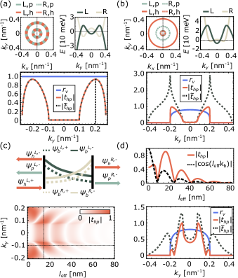
S8.2 Asymmetric junction
Once the junction is doped to different chemical potentials on each side, or the particle-hole symmetry is broken by a finite value of , the ratio of the velocity varies as changes. Moreover, the maximum of transmission is shifted away from the defined above. Nevertheless, a general form for the scattering amplitude reads
| (S20) |
where , , and do not depend on or momenta and are fixed by the doping level. The change of as a function of is hence determined by the behavior of the momentum of spinors, which we denote as , see also Sec. S3. We take real for propagating spinors [i.e. ], and imaginary for spinors bound at the interface.
For the asymmetric junction discussed in the main text, also shown in Fig. S5(b), reaches its maximum around the point where -momentum of the particle-like spinor in the -doped region vanishes, i.e. . This follows directly from the expression in Eq. (S20). Namely, we first notice that when both types of spinors are present on both sides of the junction, two momenta located at the inner branch, i.e. and have a stronger dependency on than the momenta located at the outer branch, i.e. and . Therefore, the behavior of at small is governed mostly by and in the numerator. After passes the termination points of the inner branches, and become monotonously increasing imaginary functions of (this follows from solving through analytic continuation in the complex plane). This results in an increasing numerator in Eq. (S20), while the increase in the denominator is suppressed by the reduction of lying on the outer Fermi surface in the -doped region so the monotonously grows. Furthermore, the reduction of results in a reduction of the velocity ratio until it reaches zero at that gives , see the blue line in the lower panel of Fig. S5(b). The normalized transmission amplitude , therefore, maximizes close to the vanishing point of , see the lower panel of Fig. S5(b).
Moreover, note that has a relatively large value only in a narrow range of located between the points where the inner Fermi surface of the -doped region and the outer Fermi surface of the -doped region vanish. This range can be tuned by controlling the relative size of the Fermi surfaces, which is done by tuning . Therefore, an effective spatial confinement in our system is controllable by changing the doping level of the system.
S9 Scattering at the graded interface
S9.1 Two-interface approach
The scattering amplitude through the graded interface can be calculated using a transfer matrix method, cf. Ref. [23]. Here, we use a two-interface model to describe the barrier that emerges once the chemical potential is inside the band gap. In other words, the graded interface is replaced by a gapped region having an effective length in -direction, see the upper panel in Fig. S5(c). The gapped-region is realized by replacing with in Eq. (1) – a value that sets the Fermi level to the middle of the energy gap. Solving Hamiltonian in this gapped region yields four spinors , localized at the left (L) and right (R) interface. The corresponding four momenta acquire the same absolute value i.e. , with obtained from the equation . Note that the superscript in does not carry the same physical interpretation as before where it denoted the propagating direction towards the interface, since the group velocity is not defined in the band gap. The total -matrix incorporating this gapped region is determined by the continuity conditions on the two interfaces
| (S21) |
where is the wavefuncion in the - and -doped regions defined in Eq. (S3). The wavefuncion in the gapped region is given by
| (S22) |
We insert into Eq. (S21) and solve it to obtain the scattering amplitudes and for the in-gap states as well as the amplitudes for states in the -doped region and . In the lower panel of Fig. S5(c), we show the obtained hole-to-particle transmission amplitude as a function of the length of the gapped region and . Periodic resonances of appear as a function of and we attribute them to the in-gap resonances caused by the evanescent waves. Furthermore, in the upper panel of Fig. S5(d), we show at constant , and compare it with the amplitude of the evanescent wave inside the gap. We find that the transmission amplitude follows a qualitatively identical behavior as the amplitude of the evanescent wave; with the maxima and minima being at points determined by the standing modes of the evanescent wave. The overall decay of with increasing is as well captured by the decreasing amplitudes of the evanescent waves.
S9.2 A change in the maximal transmission with increasing
Let us now turn to the dependence of when is changed. As shown in the lower panel of Fig. S5(c), for small , maximizes at nm-1, see also Sec. S8. However, when approaches , another local maximum appears at , which then grows as is increased and eventually becomes a new global maximum of at , see the lower panel of Fig. S5(d). The former occurs at that is smaller than the decaying length of the evanescent waves and, therefore, allows a higher-order scattering process to happen inside the gapped region. This leads to a strong hybridization of the evanescent states emanating from the two interfaces. The barrier in this case is relatively “transparent”, and has a maximum at the same spot as in the case without the barrier. As increases beyond the decay length of the evanescent waves, the contribution to the tunneling is dominated by the scattering between ()-doped and the gapped region. We argue that for this case, the transmission is facilitated mostly by the vanishing of , and hence the high peaks occur at .