Optical lineshapes of the C-center in silicon from ab initio calculations: Interplay of localized modes and bulk phonons
Abstract
In this work, we present a first-principles density functional theory (DFT) computational investigation of the luminescence and absorption lineshapes associated with the neutral carbon-oxygen interstitial pair () defect in silicon. We obtain the lineshapes of the defect in the dilute limit using a computational methodology that constructs dynamical matrices of supercells containing tens of thousands of atoms, utilizing systems directly accessible through DFT. Both perturbed bulk phonons and localized vibrations contribute to the phonon sideband. We achieve excellent agreement with experimental luminescence data. Our findings further reinforce the attribution of the well-known C-line in silicon to the neutral complex.
I Introduction
In recent years, quantum technologies have gained significant attention in the scientific community due to their potential applications in quantum sensing [1, 2, 3, 4], quantum communication [5, 6], and quantum computing [7, 8]. Silicon, with its established commercial success and role in solid-state devices, presents an intriguing host material for the development of future quantum technologies, with a variety of optically active point defects. These defects are of particular interest as single-photon emitters that could potentially be used for short- and long-distance exchange of information. Recent demonstrations of single photon emission from the G-center defect in silicon [9, 10, 11] has resulted in revisiting previously studied silicon defects, such as the W- [12, 13] and T-centers [14]. Due to silicon’s relatively small \qty1.1 band gap, all of these defects are active in the technologically relevant near-infrared region of light.
Carbon and oxygen atoms are among the most frequent sources of impurities in silicon. Substitutional carbon can capture silicon self-interstitials, generated by particle irradiation, and form carbon interstitials () [15]. The is mobile at room temperature [16, 17] and may capture an interstitial oxygen atom () to form the carbon-oxygen interstitial pair () complex [18], also known as C-center. It emits light at telecom wavelengths of \qty1570 (\qty0.790) [19, 20, 21] and is thus a suitable candidate for a telecom-range single-photon source compatible with fiber-optic technology, although experimental confirmation of its SPE capabilities remains absent.
The geometric configurations of the C-center defect is identified as a square-like ring within the (110) crystallographic plane, formed by two silicon atoms and two interstitials [22, 23]. Figures 1(a) and 1(b) illustrate the formation of this defect: Fig. 1(a) shows the fragment of two silicon atoms along with their nearest neighbors, while Fig. 1(b) presents the same fragment with the defect structure in place. This defect exhibits point group symmetry [21].
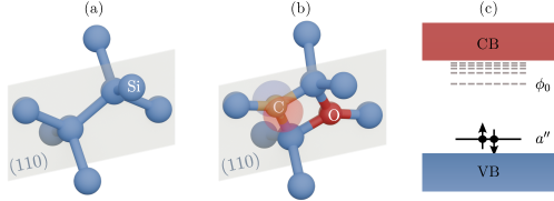
The electronic structure of the neutral C-center defect can be elucidated from the perspective of the molecular orbitals. As depicted in Fig. 1(b), both carbon and oxygen atoms form three bonds with the nearest silicon atoms, leaving four electrons to occupy two -type orbitals. For neutral centers, this configuration yields a closed-shell singlet ground state. Previous theoretical calculations predict that the only in-gap defect level (where denotes the irreducible representation of the point group) is a -type orbital localized on the carbon atom [24], while the oxygen-related -type orbital is resonant with bulk states. Although such an electronic structure suggests the absence of an intradefect transition, photoluminescence excitation measurements reveal a series of bound exciton states [20, 21]. These states arise from the interaction between a charged defect and a bound carrier, resulting in a hydrogenic wave function of the state. This, in turn, defines the single-particle energy level structure of the ground state, as illustrated in Fig. 1(c), where is the defect-induced in-gap state and denotes the first in the series of bound exciton states.
In this work we use first-principles calculations to study the thermodynamic properties, vibrational structure, and optical activity of the defect. This involves the calculation of thermodynamic parameters, including the formation energies of the most stable geometries of , , and in different charge states, the binding energy of a neutral complex, and charge-state transition levels (CTL) of , , and defects. We calculate the luminescence and absorption lineshapes of the neutral C-center in silicon. To mitigate the impact of finite-sized supercells, we employ an embedding methodology [25, 26], which allows us to simulate the vibrational structure and the adiabatic potential energy surfaces of defects in the dilute limit and model the electron–phonon coupling during an optical transition to a high degree of accuracy. The presence of resonances, bulk-like, and localized vibrational modes in our calculations explains various features of the low-temperature experimental luminescence spectrum. Furthermore, our results show that high-accuracy lineshape modeling for exciton-like excitations can be achieved using a simple approximate methodology where the excited state geometry of a neutral system is obtained by relaxing the structure of a positively charged system. Our work provides additional evidence for the correct assignment of the C-center to the carbon-oxygen interstitial pair defect. Moreover, it reinforces the idea that optical lineshape modeling can be a powerful aid in semiconductor point defect identification.
II Methods
II.1 First-principles calculations
Computations were performed using spin-polarized density functional theory (DFT), as implemented in the Vienna Ab initio Simulation Package (VASP) [27]. The projector-augmented wave (PAW) method was applied [28], with a plane-wave energy cutoff of \qty500. Brillouin zone sampling was restricted to the point. For defect modeling, we used a cubic supercell containing atomic sites ( conventional cells). Phonon calculations were carried out using the meta-GGA SCAN functional [29] to account for the exchange and correlation, while the defect formation energy calculations employed the HSE06 hybrid functional [30]. For HSE06, a default fraction () of screened Fock exchange is combined with the semilocal exchange-correlation functional of Perdew, Burke, and Ernzerhof (PBE) [31]. The above choice of functionals was motivated by their strengths: SCAN offers an optimal balance between accuracy and computational efficiency, making it ideal for capturing the structural and vibrational properties of deep-level defects [32, 33]. HSE06, with its superior accuracy in describing the band gap, was employed for defect formation energies to accurately determine thermodynamic properties.
II.2 Thermodynamic properties
The formation energy of a defect in charge state is calculated using the following formula [34]:
| (1) |
Here, is the total energy of the supercell containing the defect , and is the total energy of a defect-free supercell of the same size. The chemical potential corresponds to type atoms that have been added to () or removed from () the supercell. The Fermi energy describes the chemical potential of the electron and is referenced to the valence band maximum (VBM) . Finally, is a correction term for the electrostatic interactions between mirror images of charged defects due to periodic boundary conditions. In this work, we used the electrostatic correction scheme described in Ref. [35].
For defect complexes, an important quantity to consider is their binding energy. For a complex , composed of two defects and , the binding energy is given by
| (2) |
A positive binding energy entails that the formation of a complex is more energetically favorable than having its constituent parts exist individually. However, it should be noted that a positive value does not indicate that considerable concentrations of complexes will be formed because defect complexes generally have much smaller configurational entropies than their constituent parts [36].
Defects in solids can exist in different charge states, depending on the occupation of defect levels within the band gap. To identify the Fermi level ranges where a specific charge state is stable, we calculate the charge state transition level (CTL) [34] as
| (3) |
where denotes the formation energy of defect in the charge state with the Fermi level set to zero. The charge state is stable for Fermi levels below , while for Fermi levels above , the system stabilizes in the charge state [34]. Additionally, the ionization energy is related to the CTL, where the energy required to remove an electron from a defect in charge state and transfer it to the conduction band corresponds to the distance between the and the conduction band minimum (CBM). Conversely, the energy needed for the defect to capture an electron from the valence band while in the charge state is represented by the distance between and the VBM.
II.3 Electronic structure
Since the neutrally charged C-center defect is a closed-shell system [see Fig. 1(c)], its ground state is represented by a single determinant wave function, , where both electrons occupy the only molecular orbital located within the band-gap. In this notation, the presence (or absence) of a bar symbol denotes the spin-down (or spin-up) configuration of the molecular orbital. The electron excitation from the orbital to the bound exciton level leads to either the excited triplet or singlet state. However, reaching the triplet state requires a spin flip, making this transition dipole forbidden. The wave function of the excited triplet state in the projection is expressed as a single determinant, . In contrast, the excited singlet state is strongly correlated and expressed as a multi-determinant wave function, . The transition from the ground singlet to this excited singlet is dipole-allowed; however, this state is inaccessible via “traditional” DFT methods due to the single-determinant nature of Kohn–Sham wave functions.
The exciton-like nature of excited singlet states adds additional complexity. Modeling these states using accessible supercell sizes ( atoms) is a challenging problem because the effective radii of such single-particle states are larger than the dimensions of the supercell. Recently, a semi-ab initio method for modeling bound exciton states of deep defects was developed [37], where the authors of the paper use an effective mass model with potentials from regular DFT calculations to capture the structure of these exciton states and apply it to the negatively charged nitrogen-vacancy center in diamond. However, this approach does not allow for investigating the adiabatic potential energy surfaces (APES) required to model spectral lineshapes.
Describing the potential energy surfaces in both ground and excited electronic states is sufficient for modeling electron–phonon interactions. Based on the hypothesis that the form of the APES of a defect primarily depends on the local charge distribution of localized orbitals, we propose a simple and practical approach. In this method, we model the structural properties of the bound exciton state by considering the ground state of the positively charged defect and neglecting the contributions of exciton-like orbitals. The validity of this approach is confirmed a posteriori through comparison with experimental results. This methodology is further supported by a recent study on the defect in silicon, which similarly approximated the bound exciton state using a positively charged defect [38]. Thus, unless specified otherwise, it is assumed that the geometry of the exciton-like excited singlet state is approximated by the geometry of the positively charged defect in the ground state.
To further validate our above approach, we employed the methodology [39] to approximate the geometry of the excited singlet state by promoting an electron from the orbital in the spin-down channel to the orbital in the spin-up channel. This excitation nominally forms a triplet state. However, given that the triplet and singlet excited states share the same orbital configuration and differ only by a small exchange splitting due to the electron delocalization, which is about \qty3\milli [40, 41], the geometry of the excited triplet state should closely mirror that of the excited singlet state .
Both approaches represent limiting cases: the positively charged geometry neglects the contribution of the bound electron, while the triplet geometry overestimates the charge density due to the limited size of the supercell.
II.4 Vibrational structure and characterization of phonons
The key parameters required to compute the vibrational structure of a defect are the elements of the Hessian matrix (also known as the force constant matrix)
| (4) |
where represents the potential energy surface for ions, is the displacement of atom along direction , and is the force component on atom along direction . In this study, the Hessian matrix was computed using the finite-difference method [42], which involves calculating forces induced by small atomic displacements , systematically displacing each atom in the supercell. This approach requires a large number of single-point calculations for a defect-containing supercell with broken translational symmetry. However, the computational effort was reduced by exploiting the point-group symmetry of the system, as implemented in the phonopy software package [43, 44]. Once the Hessian matrix is obtained, diagonalization of the dynamical matrix , where and are the atomic masses, yields the mass-weighted normal modes and vibrational frequencies of the defect.
The finite-size effects inherent in supercells with atoms hinder accurate modeling of the vibrational properties of point defect systems. The use of periodic boundary conditions in these relatively small supercells artificially increases the defect concentration and restricts the representation of long-wavelength acoustic phonons. To address these limitations, we employ an advanced embedding methodology that constructs large Hessian matrices from smaller, directly accessible supercells [25, 26]. This approach leverages the short-range nature of interatomic forces, enabling the calculation of vibrational properties within much larger effective supercells by combining Hessian matrix elements from both defect-containing and bulk supercells. For a more detailed description of this methodology, we refer to Appendix A, as well as the original works in Refs. [25, 26].
Further understanding of the defect’s vibrational properties can be obtained by analyzing the “localization” of the phonon modes [45]. Bulk-like modes are spatially delocalized, resembling plane wave-like vibrations, while localized modes correspond to vibrations confined near the defect site, with frequencies outside the bulk phonon band. Between these two extremes are quasi-local modes [25], which are defect-induced vibrational resonances. These modes arise from a collection of vibrations whose energy values fall within the range of bulk phonons in the pristine material.
To quantify the phonon mode localization, we use the concept of an “inverse participation ratio” (IPR), which is defined for each phonon mode as [45, 25]
| (5) |
where is the three-dimensional mass-weighted displacement of atom , and , with representing the normalized mass-weighted displacement of atom along direction for phonon mode . The value of measures the number of oscillating atoms in vibrational mode . For example, if only a single atom vibrates for a given mode. Conversely, if all atoms in the supercell participate equally in the vibration. For intermediate cases, where only atoms vibrate appreciably, . A constant as a function of the supercell size characterizes a truly localized mode. This behavior occurs because the frequency of the localized mode lies outside the bulk phonon band, and the mode’s spatial profile remains independent of the density or presence of bulk phonons.
While IPR provides a quantitative measure of phonon mode localization, it is more convenient to work with the “localization ratio” of phonon mode [25]:
| (6) |
As seen from this definition, the larger the ratio , the more localized the phonon mode is.
II.5 Optical lineshapes and electron–phonon coupling parameters
In the Franck–Condon and adiabatic approximations, the normalized lineshape for the absorption and emission spectra of a semiconductor defect as a function of frequency at is given by [26]
| (7) | ||||
| (8) |
where is a normalization constant, is the zero-phonon line (ZPL) energy, and and are the vibrational wave functions of the initial () and final () electronic states. Here, is the energy of the -th vibrational state in the final electronic manifold with respect to the potential energy minima. The minus and plus signs in the argument of the -function correspond to emission and absorption, respectively, with the parameter taking the value of for emission and for absorption. The optical spectral function quantifies the transition amplitudes between vibrational states and is central in determining the lineshape.
To simplify the calculation of the overlap integrals in Eq. (8), we adopt the equal-mode approximation [26, 46], which assumes that the vibrational modes of the initial and final states are identical. To address the limitations of this assumption, we follow Ref. [26] and consistently employ the vibrational modes of the final state, using the ground state phonons for emission and the excited state phonons for absorption.
Efficient estimation of the optical spectral function can be obtained by computing it in the time domain through the generating function method of Kubo and Lax [47, 48]. In this approach, the spectral function is obtained from the generating function via the relation
| (9) |
The term is introduced as a phenomenological correction to account for the homogeneous Lorentzian broadening of the ZPL not captured by the theory, as well as to address inhomogeneous broadening. In practice, parameter is adjusted to match the experimental linewidth of the ZPL.
In the equal mode approximation, the generating function can be expressed as
| (10) |
where the plus sign in the exponent is used for emission and the minus sign for absorption, represents the partial Huang–Rhys (HR) factor, and the summation runs over all vibrational modes of the system. The factor quantifies the average number of excited phonons during an optical transition [49]. It is defined as
| (11) |
where represents the ionic displacement along the normal mode induced by an optical transition. Specifically, is the projection of the mass-weighted displacement between the ground and excited states onto the normalized phonon mode :
| (12) |
Here, is the displacement of the atom along the coordinate, and is its mass.
A primary challenge in evaluating Eq. (10) for extended systems, such as defects, is that the electron–phonon coupling must account for a continuum of vibrational frequencies. To address this and achieve a converged, continuous description of the electron–phonon interaction, we first define the spectral density of the electron–phonon coupling (also known as the spectral function of electron–phonon coupling) as
| (13) |
which allows us to rewrite the generating function as follows:
| (14) |
Here, is the total HR factor, where the sum is evaluated over all vibrational modes of the defect system. We employ smoothing functions tailored to different mode types to approximate the -functions in Eq. (13). For bulk-like and quasi-localized modes, -functions are replaced with Gaussians of specified width, which allows controlled spectral broadening. For highly localized modes, we instead use Lorentzians, with half-width at full maximum (HWHM) chosen to accurately capture the side peaks in the optical lineshape. For a given spectral resolution, we apply the embedding methodology and check the convergence of the optical lineshape as a function of the supercell size (see Fig. A1 in Appendix A for an illustration). Usually, the convergence is achieved with a system size greater than atoms.
An additional complication in supercell calculations arises when determining the relaxation profile following an optical transition. The small supercell size in direct calculations suppresses the long-wavelength components of in Eq. (12). To accurately capture the relaxation profile in the dilute limit, we calculate for each vibrational mode of a large supercell (obtained via the embedding procedure) by using forces and the harmonic relation to displacements. The relaxation component is then evaluated as
| (15) |
where represents the force on atom along direction when the system is in the final electronic state but remains in the equilibrium geometry of the initial state calculated in the directly accessible supercell. Meanwhile, represents the vibrational mode shape as obtained in the embedded supercell. With the forces already converged within the explicitly accessible supercell, this approach, combined with the embedding methodology, effectively captures the electron–phonon coupling for low-frequency modes and provides an accurate description of the optical lineshapes.
III Results and discussion
III.1 Lattice parameters and band gaps
We begin by calculating the lattice constants and band gaps of pure silicon using the geometry relaxation procedures with PBE, SCAN, and HSE06 functionals. Table 1 compares these results with low-temperature experimental values [50, 51].
The SCAN functional yields the best agreement with the experimental lattice constant, providing the value of with an absolute deviation of \qty0.009. In comparison, the HSE06 functional produces the lattice constant of with an absolute deviation of \qty0.014, while the PBE functional overestimates this parameter, yielding with a deviation of \qty0.050. Regarding the band gaps, the HSE06 functional shows the best agreement with the experiment, with an absolute deviation of \qty0.017 and a value of . PBE and SCAN underestimate the band gap by \qty0.559 and \qty0.345, respectively, a common feature of semilocal functionals. Based on the above results, the SCAN functional was selected for defect phonon and relaxation profile calculations due to its accuracy in predicting structural parameters and computational efficiency [32]. The more computationally demanding HSE06 functional was used exclusively for formation energy calculations.
III.2 Thermodynamic properties
The calculated formation energies of neutral , , and defects are summarized in Table 2, alongside comparisons to previous studies. These values were calculated using Eq. (1), with the chemical potentials for Si, C, and O obtained from silicon, diamond, and -quartz (SiO2), respectively. To our knowledge, experimental reference data for defect formation energies are limited. However, a key comparison is available for the defect from Ref. [52].
In the case of the neutral defect, we considered three distinct geometrical configurations, following Ref. [57]: the dumbbell, the dumbbell, and the bond-centered . In agreement with the results from Refs. [58, 59, 57, 38], our calculations indicate that the dumbbell configuration is the most energetically favorable. The formation energy values of \qty3.49 and \qty3.70 were obtained using the SCAN and HSE06 functionals, respectively. The calculated formation energies of the and bond-centered configurations are larger by \qty0.55 (\qty0.49) and \qty0.70 (\qty0.81) using the SCAN (HSE06) functional. Unless otherwise specified, the in the remainder of this text refers to the dumbbell configuration.
The calculated formation energy values of the neutral defect become \qty1.79 and \qty1.81 for the SCAN and HSE06 functionals, respectively. These values are consistent with the upper limit of the \qty1.65(15) experimental value from Ref. [52], thereby validating the accuracy of our computational methodologies.
By applying Eq. 2 and utilizing the data from Table 2, the calculated binding energies of the neutral complex are \qty1.53 and \qty1.56 for the SCAN and HSE06 functionals, respectively. These values show good agreement with previous theoretical studies [53, 55, 60], which report binding energies in the range of \qty1.6 to \qty1.7.
Finally, Table 3 and Fig. 2 present the CTLs of the and defects in silicon obtained using the HSE06 functional. Our results are compared with previous theoretical studies from Refs. [53, 24, 38], as well as with available experimental data from Refs. [61, 62, 63]. Notably, our calculations indicate no energy levels within the band gap for the defect; therefore, no CTL data for this defect is presented.
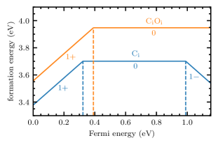
For the defect, the HSE06 functional yielded a donor CTL at \qty0.32 above the VBM, which aligns well with the experimental value of \qty0.28 [61]. The calculated acceptor transition level is positioned at \qty0.16 below the CBM, showing good agreement with the experimental value of \qty0.10 [61].
For the complex, the HSE06 calculations predict a donor CTL at \qty0.39 above the VBM, which agrees well with experimental values of \qty0.38 and \qty0.36 [62, 63]. Furthermore, this result is consistent with earlier theoretical predictions of Refs. [53, 24], which place the transition levels at \qty0.41 and \qty0.36 above the VBM, respectively.
The computed formation energy of the complex is relatively high. Assuming that defect concentrations are established at the silicon melting point (\qty1687), the equilibrium density of is expected to remain below \qtye12\per\cubic. Furthermore, during the cooling of the sample, if is mobile, it can bind with to form the complex due to the relatively high and positive binding energy of the complex, which further increases the density of centers. However, defects are typically formed under non-equilibrium conditions, such as during irradiation, which leads to a higher defect density [15].
The ionization threshold energy is given by (using the experimental value for ), which represents the theoretical upper bound for the ZPL energy. According to theoretical estimates in Ref. [21], the binding energy of the lowest bound exciton level is about \qty40\milli, predicting a ZPL energy of \qty0.74. This prediction shows good agreement with the experimental ZPL value of \qty0.790.
III.3 Vibrational structures
Figure 3(a) presents the calculated localization ratios () for the symmetry vibrational modes (blue) of the ground state alongside normalized experimental luminescence data (gray) from Ref. [64]. Higher values indicate modes with more localized vibration amplitudes near the defect. The vibrational modes are not shown, as they do not contribute to the linear electron–phonon interaction due to symmetry constraints. The smaller inset figure overlays the phonon density of states (DOS) for pristine silicon (red) with the experimental luminescence spectrum. Note that the horizontal axis in both the main and the inset figures represents the energy shift relative to the ZPL. The vibrational modes of the defect system were computed using an embedding methodology to construct a supercell ( atomic sites), while the DOS was calculated for a bulk silicon supercell ( atomic sites), both employing the SCAN functional. The embedding parameters and convergence with respect to the supercell size are discussed in Appendix A.
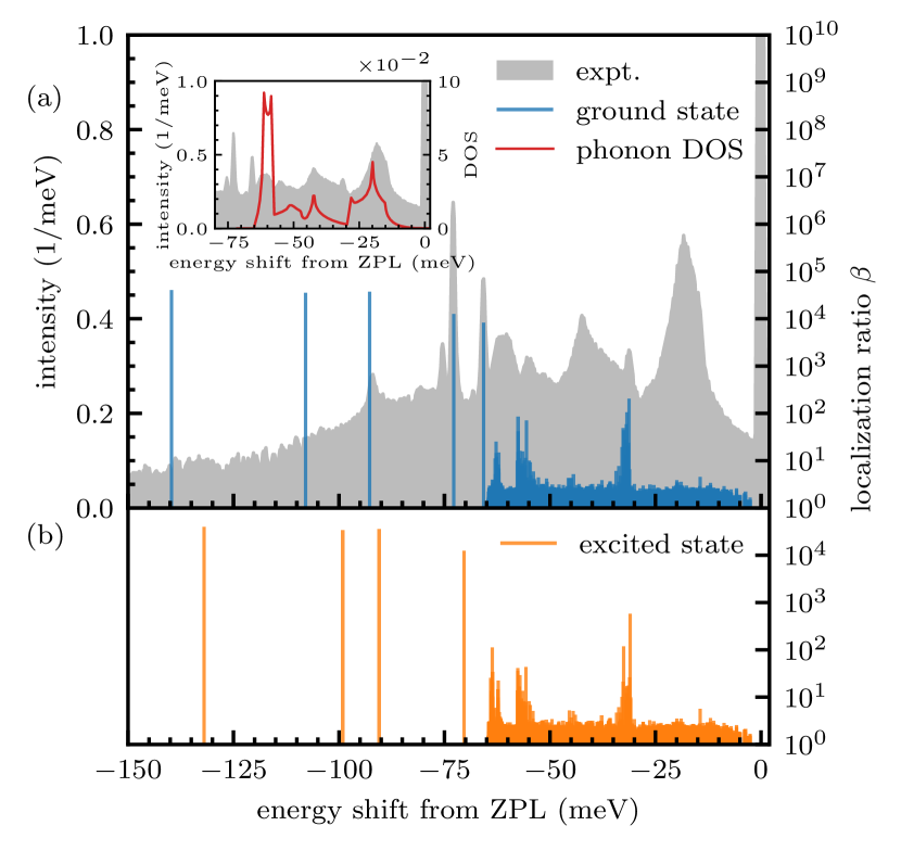
In Fig. 3(a), localized vibrational modes with high localization ratios () are identified at energies of \qtylist65.8;72.8;92.7;107.9;139.7\milli. Their corresponding atomic displacements, considering only nearest neighbors, are illustrated in Figs. 4(a)–(e). Notably, the modes at \qtylist65.8;72.8;92.7\milli [Figs. 4(a)–(c)] show a strong correlation with pronounced peaks in the sideband of the experimental emission spectrum. In contrast, the lack of luminescence peaks at \qtylist107.9;139.7\milli suggests that high values alone do not necessarily correlate with significant electron–phonon coupling; the mode must also effectively project onto the relaxation profile after the optical transition, as described by Eq. (12). Figure 4(f) illustrates the calculated equilibrium geometry change following the excitation, where the positively charged state approximates the excited singlet state of the neutral defect.
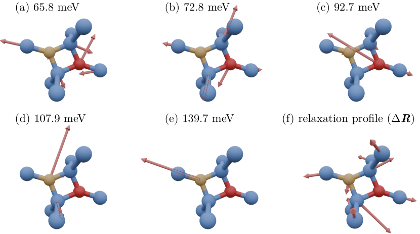
The modes visible in the emission spectrum, particularly those at \qtylist65.8;72.8;92.7\milli, exhibit considerable vibrational amplitudes on the oxygen atom and adjacent silicon atoms [see Figs. 4(a)–(c)]. Although the oxygen atom undergoes minimal displacement in the relaxation profile shown in Fig. 4(f), the neighboring silicon atoms experience notable geometry changes. These displacements align well with the vibrational amplitudes of the \qtylist65.8;72.8\milli modes and, to a lesser extent, the \qty92.7\milli mode. In contrast, the higher-frequency modes at \qtylist107.9;139.7\milli [see Figs. 4(d) and 4(e)] predominantly involve vibrations centered on the carbon atom, which undergoes only a minor geometry shift during the optical transition, with minimal mode participation onto the neighboring silicon atoms. This observation qualitatively explains the absence of corresponding features for these higher-frequency modes in the experimental luminescence spectrum.
Beyond the localized vibrations, Fig. 3(a) reveals other distinct classes of vibrational modes. The first category, identified as vibrational resonances, appears as collections of quasi-localized vibrations centered around \qtylist32;54;62\milli. These modes are characterized by values and can be tentatively associated with corresponding features in the experimental spectrum, indicating their potential role in coupling with electronic transitions.
In contrast, bulk-like modes, characterized by relatively small values (), extend to energies of about \qty65\milli from the ZPL, corresponding to the phonon band edge in pristine silicon. These modes primarily reflect the collective vibrational characteristics of the silicon lattice and, therefore, are present in both pure and defect-containing systems. Notably, bulk-like modes at energies around \qtylist20;42\milli exhibit peaks in the phonon DOS function on the low-energy side of the ZPL [see inset of Fig. 3(a)]. These peaks coincide with features in the experimental luminescence spectrum, emphasizing the bulk-like character of these modes and their influence on the observed spectrum.
In Fig. 3(b), we present the frequencies and localization factors of vibrational modes calculated for the positively charged defect, which approximates the excited state’s structural properties. A comparison between Fig. 3(a) and Fig. 3(b) reveals a pronounced lowering in the vibrational frequencies of localized modes. Most notably, the mode observed at \qty65.8\milli in the ground state shifts to a frequency below the bulk phonon band maximum in the excited state, transitioning into a vibrational resonance. In contrast, the quasi-localized vibrations at \qtylist32;54;62\milli remain at nearly the same energies in both ground and excited states. This significant frequency shift of localized modes indicates a notable quadratic electron–phonon interaction, which we do not address in this study.
The above analysis shows that the C-center’s optical sideband features can be characterized by examining different vibrational modes. However, comprehensive calculations of the electron–phonon coupling during optical processes are necessary to obtain a deeper understanding of how these modes affect the spectral lineshapes.
III.4 Optical lineshapes
In the final part of this study, we analyze the theoretical optical lineshapes of the C-center in silicon. The accurate calculation of these lineshapes requires electron–phonon coupling parameters, which were computed using the same supercell size, exchange-correlation functional, and vibrational modes as those described in Section III.3.
First, by analyzing the calculated partial HR factors [see Eq. (11)] pertaining to localized modes, we observe significant contributions from the localized vibrational modes at \qtylist65.8;72.8;92.7\milli [Figs. 3(a)–(c)], with corresponding HR factors of , respectively. In contrast, vibrational modes involving primarily the carbon atom exhibit much weaker electron–phonon interaction. Indeed, the \qty107.9\milli mode has a near-negligible HR factor of , while the \qty139.7\milli mode shows limited coupling, with an HR factor of . This distinction is illustrated in the spectral function of electron–phonon coupling shown in the inset of Fig. 5, where the participation of modes above \qty65\milli is depicted by Lorentzian-type sharp peaks.
In the inset of Fig. 5, we present the spectral density of the electron–phonon coupling during emission. This function was calculated using Eq. (13), where the -functions for phonon modes below \qty65\milli were replaced with Gaussians, each with a width of . For the localized modes above \qty65\milli, Lorentzians were employed, characterized by a half-width at half-maximum (HWHM) of . Regarding the electron–phonon interaction with both resonant and bulk-like vibrational modes, the spectral function displays five distinct peaks below \qty65\milli. The peaks at \qtylist20;42\milli arise from the high density of bulk-like modes, while the remaining three originate from the interactions with quasi-localized vibrational resonances. The effective shapes of these collective vibrations are presented in Appendix B.
Figure 5 presents the calculated luminescence lineshape (blue), obtained using Eqs. (7) and (9), in comparison with normalized experimental luminescence data (gray) from Ref. [64]. The homogeneous broadening parameter, , was set to . The horizontal axis is shifted relative to the ZPL, similarly to Fig. 3. The convergence of both the spectral function and the luminescence lineshape with respect to supercell size is discussed in detail in Appendix A.
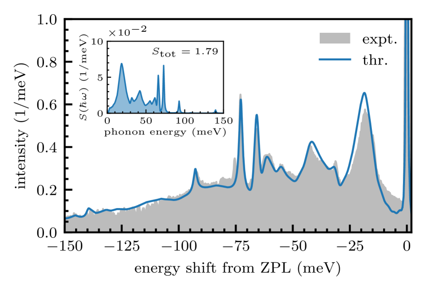
The calculated emission lineshape in Fig. 5 demonstrates remarkable agreement with the experimental data. Various features in the theoretical spectrum, arising from different modes, align well with the peaks and dips observed in the experiment. The relative intensities of these features are described accurately as well. The localized modes at \qtylist65.8;72.8;92.7\milli and the resonances at around \qtylist32;54;62\milli relative to the ZPL are clearly replicated in the theoretical lineshape and correspond to pronounced peaks in the experiment. The influence of bulk phonons is evident through broad peaks at around \qtylist20;42\milli from to the ZPL. The total HR factor for the emission is calculated to be , while the Debye–Waller (DW) factor , which specifies the relative weight of the intensity of the ZPL, is estimated to be about \qty20.
While the overall agreement of the calculated emission spectrum with the experimental data is outstanding, some discrepancies are found. The main one is the absence of a sharp peak and its shoulder in the calculated lineshape at around \qty76\milli from the ZPL; the origin of this feature remains an open question.
Figure 6 presents the calculated absorption lineshape (orange) compared to the computed luminescence lineshape (blue) from Fig. 5. The latter is inverted with respect to the ZPL for comparison. The horizontal axis is shifted relative to the ZPL. The inset figure compares the spectral functions of the electron–phonon coupling during absorption and luminescence. The calculated absorption lineshape corresponds to the same system size and functional as in Fig. 5, but with the vibrational modes of the excited state as opposed to those of the ground state in the case of luminescence.
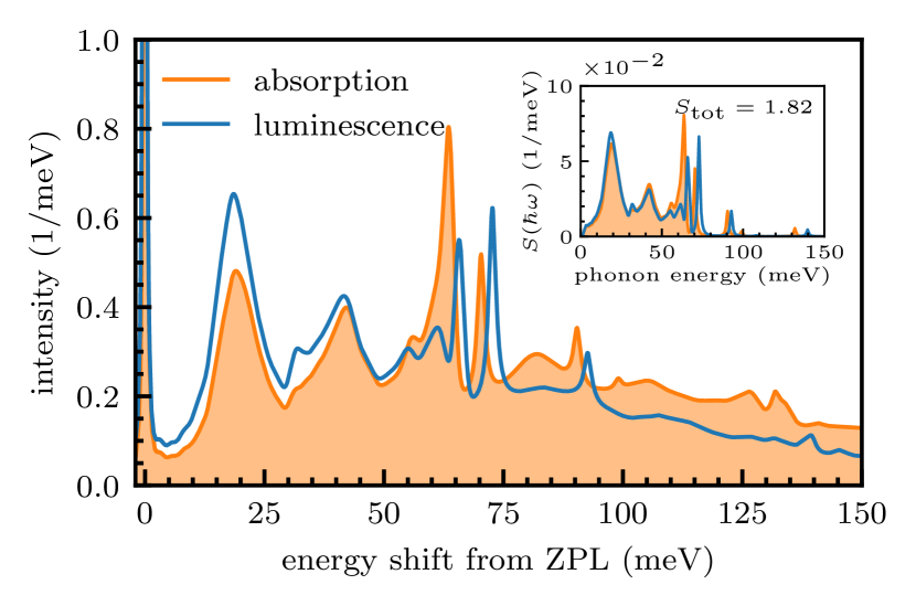
Upon comparing the calculated absorption and emission lineshapes, along with the corresponding spectral functions presented in the inset, it is evident that the spectra exhibit qualitative similarities, particularly within approximately \qty60\milli of the ZPL. Beyond this threshold, the energies of the peaks in the absorption lineshape, influenced by the localized modes, shift to lower values compared to the corresponding peaks in the luminescence lineshape. Notably, the localized modes at \qtylist70.3;90.4;99.0;131.8\milli are clearly involved in the absorption process. The total HR factor for absorption is calculated to be , which is comparable to the value of for luminescence. This similarity indicates that the vibrational structures of both the ground and excited states are closely aligned regarding the phonons’ forms and energies.
The disparity in the relative spectral weights of luminescence and absorption lineshapes can be attributed to the prefactor in Eq. (7). In the context of luminescence, where , this leads to a more pronounced increase in the weight of the lineshape near the ZPL compared to absorption, which is characterized by . Consequently, this results in a substantial asymmetry between the two spectra, as illustrated in Fig. 6. Conversely, the asymmetry observed in the electron–phonon coupling functions (see inset of Fig. 6) is comparatively less pronounced and arises purely from the differences in the vibrational modes between the ground and excited states.
When analyzing the theoretical absorption lineshape of the C-center, it is important to recognize that the actual absorption in bulk silicon may differ from the calculated bound-to-bound transitions. This discrepancy arises because the ionization threshold, which marks the onset of electron promotion into the conduction band continuum, lies only a few tens of \unit\milli above the ZPL. Specifically, Ref. [21] estimates this threshold to be just \qty38\milli above the ZPL. Consequently, the actual absorption spectrum should reflect a convolution of both the photoionization and the bound-to-bound absorption cross-sections. Nevertheless, we anticipate that some of the sharp features in the theoretical lineshape may still be observable in experimental absorption measurements.
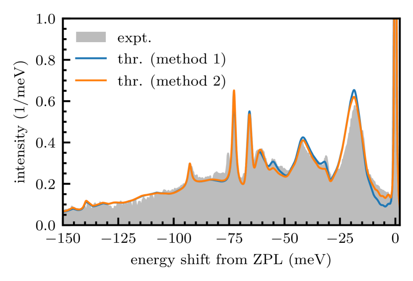
As previously discussed, the calculated lineshapes presented in this study were obtained by modeling the structural properties of the exciton-like excited singlet state using the geometry of the positively charged defect in its ground state. In Fig. 7, we compare the luminescence lineshape from this approach (method 1) with that obtained using the methodology (method 2), in which the excited triplet state is used as an approximate model for the excited singlet state . Additionally, these theoretical lineshapes are compared with the experimental emission data from Ref. [64]. Both theoretical approaches yield almost identical results and show excellent agreement with the experimental data. However, some discrepancies are observed between the two methodologies. The first is in the treatment of acoustic phonons near the ZPL, where method 2 provides a more accurate description. The second discrepancy involves the resonances at \qtylist32;54\milli from the ZPL, where method 1 offers a better description. A common feature of these methods is the failure to describe the sharp peak and its shoulder at around \qty76\milli from the ZPL in the experimental data.
IV Conclusions
In this work, we have calculated the thermodynamic properties of and interstitials, and the complex, commonly referred to as the C-center, achieving good agreement with the experimental data and previous theoretical studies. By applying an advanced embedding methodology, which enables the precise modeling of a defect’s phonon structure in the dilute limit, we have accurately characterized the vibrational structure of the C-center in silicon. This approach offers deep insights into the electron–phonon interactions of this defect complex, uncovering a complicated interplay between localized and bulk-like phonon modes. These modes, in turn, collectively influence the intricate luminescence lineshape of the C-center, characterized by many localized vibrational modes and resonances. Our calculated theoretical lineshape exhibits outstanding correspondence with the low-temperature experimental emission data, successfully reproducing nearly all the features observed in the latter. This substantial agreement further supports the assignment of the experimental \qty790\milli line to the complex.
Furthermore, we demonstrated that the transitions involving single exciton-like states can be effectively modeled by approximating the geometry of the bound exciton state with that of a charged defect while neglecting the contribution of the bound electron in the hydrogenic orbital. This approximation simplifies the analysis of optical lineshapes for such transitions without compromising accuracy. Therefore, our work advances modern methodologies for precisely describing the optical properties of defects exhibiting exciton-like states within a first-principles computational framework. This advancement enhances the ability to identify defects, particularly in the search for those with potential applications in quantum technologies.
Acknowledgements
Financial support was kindly provided by the Research Council of Norway and the University of Oslo through the frontier research project QuTe (no. 325573, FriPro ToppForsk-program). Computational resources were provided by the supercomputer GALAX of the Center for Physical Sciences and Technology (FTMC), Vilnius, Lithuania, and the High Performance Computing Center “HPC Saulėtekis” in the Faculty of Physics, Vilnius University, Lithuania.
References
- Degen et al. [2017] C. L. Degen, F. Reinhard, and P. Cappellaro, Quantum sensing, Rev. Mod. Phys. 89, 035002 (2017).
- Le Sage et al. [2013] D. Le Sage, K. Arai, D. R. Glenn, S. J. DeVience, L. M. Pham, L. Rahn-Lee, M. D. Lukin, A. Yacoby, A. Komeili, and R. L. Walsworth, Optical magnetic imaging of living cells, Nat. 496, 486 (2013).
- Rondin et al. [2014] L. Rondin, J.-P. Tetienne, T. Hingant, J.-F. Roch, P. Maletinsky, and V. Jacques, Magnetometry with nitrogen-vacancy defects in diamond, Rep. Prog. Phys. 77, 056503 (2014).
- Vindolet et al. [2022] B. Vindolet, M.-P. Adam, L. Toraille, M. Chipaux, A. Hilberer, G. Dupuy, L. Razinkovas, A. Alkauskas, G. Thiering, A. Gali, M. De Feudis, M. W. Ngandeu Ngambou, J. Achard, A. Tallaire, M. Schmidt, C. Becher, and J.-F. Roch, Optical properties of SiV and GeV color centers in nanodiamonds under hydrostatic pressures up to 180 GPa, Phys. Rev. B 106, 214109 (2022).
- Gisin and Thew [2007] N. Gisin and R. Thew, Quantum communication, Nat. Photonics 1, 165 (2007).
- Al-Juboori et al. [2023] A. Al-Juboori, H. Z. J. Zeng, M. A. P. Nguyen, X. Ai, A. Laucht, A. Solntsev, M. Toth, R. Malaney, and I. Aharonovich, Quantum key distribution using a quantum emitter in hexagonal boron nitride, Adv. Quantum Tech. 6, 2300038 (2023).
- Ladd et al. [2010] T. D. Ladd, F. Jelezko, R. Laflamme, Y. Nakamura, C. Monroe, and J. L. O’Brien, Quantum computers, Nat. 464, 45 (2010).
- Weber et al. [2010] J. R. Weber, W. F. Koehl, J. B. Varley, A. Janotti, B. B. Buckley, C. G. Van De Walle, and D. D. Awschalom, Quantum computing with defects, Proc. Natl. Acad. Sci. 107, 8513 (2010).
- Hollenbach et al. [2020] M. Hollenbach, Y. Berencén, U. Kentsch, M. Helm, and G. V. Astakhov, Engineering telecom single-photon emitters in silicon for scalable quantum photonics, Opt. Express 28, 26111 (2020).
- Redjem et al. [2020] W. Redjem, A. Durand, T. Herzig, A. Benali, S. Pezzagna, J. Meijer, A. Yu. Kuznetsov, H. S. Nguyen, S. Cueff, J.-M. Gérard, I. Robert-Philip, B. Gil, D. Caliste, P. Pochet, M. Abbarchi, V. Jacques, A. Dréau, and G. Cassabois, Single artificial atoms in silicon emitting at telecom wavelengths, Nat. Electron. 3, 738 (2020).
- Durand et al. [2021] A. Durand, Y. Baron, W. Redjem, T. Herzig, A. Benali, S. Pezzagna, J. Meijer, A. Yu. Kuznetsov, J.-M. Gérard, I. Robert-Philip, M. Abbarchi, V. Jacques, G. Cassabois, and A. Dréau, Broad diversity of near-infrared single-photon emitters in silicon, Phys. Rev. Lett. 126, 083602 (2021).
- Buckley et al. [2020] S. M. Buckley, A. N. Tait, G. Moody, B. Primavera, S. Olson, J. Herman, K. L. Silverman, S. Papa Rao, S. Woo Nam, R. P. Mirin, and J. M. Shainline, Optimization of photoluminescence from W centers in silicon-on-insulator, Opt. Express 28, 16057 (2020).
- Baron et al. [2022] Y. Baron, A. Durand, P. Udvarhelyi, T. Herzig, M. Khoury, S. Pezzagna, J. Meijer, I. Robert-Philip, M. Abbarchi, J.-M. Hartmann, V. Mazzocchi, J.-M. Gérard, A. Gali, V. Jacques, G. Cassabois, and A. Dréau, Detection of single W-centers in silicon, ACS Photonics 9, 2337 (2022).
- Dhaliah et al. [2022] D. Dhaliah, Y. Xiong, A. Sipahigil, S. M. Griffin, and G. Hautier, First-principles study of the T center in silicon, Phys. Rev. Materials 6, L053201 (2022).
- Zhao et al. [1996] S. Zhao, A. M. Agarwal, J. L. Benton, G. H. Gilmer, and L. C. Kimerling, Interstitial defect reactions in silicon, MRS Proc. 442, 231 (1996).
- Noonan et al. [1976] J. R. Noonan, C. G. Kirkpatrick, and B. G. Streetman, Photoluminescence from Si irradiated with 1.5-MeV electrons at 100∘K, J. Appl. Phys. 47, 3010 (1976).
- Kimerling et al. [1989] L. C. Kimerling, M. T. Asom, J. L. Benton, P. J. Drevinsky, and C. E. Caefer, Interstitial defect reactions in silicon, Mater. Sci. Forum 38–41, 141 (1989).
- Davies [1989] G. Davies, The optical properties of luminescence centres in silicon, Phys. Rep. 176, 83 (1989).
- Spry and Compton [1968] R. J. Spry and W. D. Compton, Recombination luminescence in irradiated silicon, Phys. Rev. 175, 1010 (1968).
- Wagner et al. [1984] J. Wagner, K. Thonke, and R. Sauer, Excitation spectroscopy on the 0.79-eV (C) line defect in irradiated silicon, Phys. Rev. B 29, 7051 (1984).
- Thonke et al. [1985] K. Thonke, A. Hangleiter, J. Wagner, and R. Sauer, 0.79 eV (C line) defect in irradiated oxygen-rich silicon: Excited state structure, internal strain and luminescence decay time, J. Phys. C: Solid State Phys. 18, L795 (1985).
- Trombetta and Watkins [1987] J. M. Trombetta and G. D. Watkins, Identification of an interstitial carbon - interstitial oxygen complex in silicon, MRS Proc. 104, 93 (1987).
- Jones and Öberg [1992] R. Jones and S. Öberg, Oxygen frustration and the interstitial carbon-oxygen complex in Si, Phys. Rev. Lett. 68, 86 (1992).
- Udvarhelyi et al. [2022] P. Udvarhelyi, A. Pershin, P. Deák, and A. Gali, An L-band emitter with quantum memory in silicon, npj Comput. Mater. 8, 262 (2022).
- Alkauskas et al. [2014] A. Alkauskas, B. B. Buckley, D. D. Awschalom, and C. G. Van de Walle, First-principles theory of the luminescence lineshape for the triplet transition in diamond NV centres, New J. Phys. 16, 073026 (2014).
- Razinkovas et al. [2021] L. Razinkovas, M. W. Doherty, N. B. Manson, C. G. Van de Walle, and A. Alkauskas, Vibrational and vibronic structure of isolated point defects: The nitrogen-vacancy center in diamond, Phys. Rev. B 104, 045303 (2021).
- Kresse and Furthmüller [1996] G. Kresse and J. Furthmüller, Efficient iterative schemes for ab initio total-energy calculations using a plane-wave basis set, Phys. Rev. B 54, 11169 (1996).
- Blöchl [1994] P. E. Blöchl, Projector augmented-wave method, Phys. Rev. B 50, 17953 (1994).
- Sun et al. [2015] J. Sun, A. Ruzsinszky, and J. P. Perdew, Strongly constrained and appropriately normed semilocal density functional, Phys. Rev. Lett. 115, 036402 (2015).
- Heyd et al. [2003] J. Heyd, G. E. Scuseria, and M. Ernzerhof, Hybrid functionals based on a screened Coulomb potential, J. Chem. Phys. 118, 8207 (2003).
- Perdew et al. [1996] J. P. Perdew, K. Burke, and M. Ernzerhof, Generalized gradient approximation made simple, Phys. Rev. Lett. 77, 3865 (1996).
- Maciaszek et al. [2023] M. Maciaszek, V. Žalandauskas, R. Silkinis, A. Alkauskas, and L. Razinkovas, The application of the SCAN density functional to color centers in diamond, J. Chem. Phys. 159, 084708 (2023).
- Silkinis et al. [2024] R. Silkinis, V. Žalandauskas, G. Thiering, A. Gali, C. G. Van De Walle, A. Alkauskas, and L. Razinkovas, Optical lineshapes for orbital singlet to doublet transitions in a dynamical Jahn-Teller system: The NiV center in diamond, Phys. Rev. B 110, 075303 (2024).
- Freysoldt et al. [2014] C. Freysoldt, B. Grabowski, T. Hickel, J. Neugebauer, G. Kresse, A. Janotti, and C. G. Van de Walle, First-principles calculations for point defects in solids, Rev. Mod. Phys. 86, 253 (2014).
- Freysoldt et al. [2009] C. Freysoldt, J. Neugebauer, and C. G. Van de Walle, Fully ab initio finite-size corrections for charged-defect supercell calculations, Phys. Rev. Lett. 102, 016402 (2009).
- Van de Walle and Neugebauer [2004] C. G. Van de Walle and J. Neugebauer, First-principles calculations for defects and impurities: Applications to III-nitrides, J. Appl. Phys. 95, 3851 (2004).
- Chen et al. [2024] Y. Chen, L. Oberg, J. Flick, A. Lozovoi, C. A. Meriles, and M. W. Doherty, Semiempirical ab initio modeling of bound states of deep defects in semiconductor quantum technologies, Phys. Rev. B 109, L201115 (2024).
- Deák et al. [2024] P. Deák, S. Li, and A. Gali, Quantum bit with telecom wave-length emission from a simple defect in Si, Commun. Phys. 7, 337 (2024).
- Gali et al. [2009] A. Gali, E. Janzén, P. Deák, G. Kresse, and E. Kaxiras, Theory of spin-conserving excitation of the N–V center in diamond, Phys. Rev. Lett. 103, 186404 (2009).
- Bohnert et al. [1993] G. Bohnert, K. Weronek, and A. Hangleiter, Transient characteristics of isoelectronic bound excitons at hole-attractive defects in silicon: The C(0.79 eV), P(0.767 eV), and H(0.926 eV) lines, Phys. Rev. B 48, 14973 (1993).
- Ishikawa et al. [2011] T. Ishikawa, K. Koga, T. Itahashi, K. M. Itoh, and L. S. Vlasenko, Optical properties of triplet states of excitons bound to interstitial-carbon interstitial-oxygen defects in silicon, Phys. Rev. B 84, 115204 (2011).
- Kresse et al. [1995] G. Kresse, J. Furthmüller, and J. Hafner, Ab Initio force constant approach to phonon dispersion relations of diamond and graphite, Europhys. Lett. 32, 729 (1995).
- Togo [2023] A. Togo, First-principles phonon calculations with phonopy and phono3py, J. Phys. Soc. Jpn. 92, 012001 (2023).
- Togo et al. [2023] A. Togo, L. Chaput, T. Tadano, and I. Tanaka, Implementation strategies in phonopy and phono3py, J. Phys.: Condens. Matter 35, 353001 (2023).
- Bell et al. [1970] R. J. Bell, P. Dean, and D. C. Hibbins-Butler, Localization of normal modes in vitreous silica, germania and beryllium fluoride, J. Phys. C: Solid State Phys. 3, 2111 (1970).
- Markham [1959] J. J. Markham, Interaction of normal modes with electron traps, Rev. Mod. Phys. 31, 956 (1959).
- Kubo and Toyozawa [1955] R. Kubo and Y. Toyozawa, Application of the method of generating function to radiative and non-radiative transitions of a trapped electron in a crystal, Prog. Theor. Phys. 13, 160 (1955).
- Lax [1952] M. Lax, The Franck–Condon principle and its application to crystals, J. Chem. Phys. 20, 1752 (1952).
- Huang and Rhys [1950] K. Huang and A. Rhys, Theory of light absorption and non-radiative transitions in F-centres, Proc. R. Soc. Lond. A 204, 406 (1950).
- Batchelder and Simmons [1964] D. N. Batchelder and R. O. Simmons, Lattice constants and thermal expansivities of silicon and of calcium fluoride between 6∘ and 322∘K, J. Chem. Phys. 41, 2324 (1964).
- Bludau et al. [1974] W. Bludau, A. Onton, and W. Heinke, Temperature dependence of the band gap of silicon, J. Appl. Phys. 45, 1846 (1974).
- Bean and Newman [1971] A. R. Bean and R. C. Newman, The solubility of carbon in pulled silicon crystals, J. Phys. Chem. Solids 32, 1211 (1971).
- Coutinho et al. [2001] J. Coutinho, R. Jones, P. R. Briddon, S. Öberg, L. I. Murin, V. P. Markevich, and J. L. Lindström, Interstitial carbon-oxygen center and hydrogen related shallow thermal donors in Si, Phys. Rev. B 65, 014109 (2001).
- Wang et al. [2014] H. Wang, A. Chroneos, C. A. Londos, E. N. Sgourou, and U. Schwingenschlögl, Carbon related defects in irradiated silicon revisited, Sci. Rep. 4, 4909 (2014).
- Hao et al. [2004a] S. Hao, L. Kantorovich, and G. Davies, The interstitial CiOi defect in bulk Si and SiGe, J. Phys.: Condens. Matter 16, 8545 (2004a).
- Hao et al. [2004b] S. Hao, L. Kantorovich, and G. Davies, Interstitial oxygen in Si and Si Ge, Phys. Rev. B 69, 155204 (2004b).
- Zirkelbach et al. [2011] F. Zirkelbach, B. Stritzker, K. Nordlund, J. K. N. Lindner, W. G. Schmidt, and E. Rauls, Combined ab initio and classical potential simulation study on silicon carbide precipitation in silicon, Phys. Rev. B 84, 064126 (2011).
- Watkins and Brower [1976] G. D. Watkins and K. L. Brower, EPR observation of the isolated interstitial carbon atom in silicon, Phys. Rev. Lett. 36, 1329 (1976).
- Song and Watkins [1990] L. W. Song and G. D. Watkins, EPR identification of the single-acceptor state of interstitial carbon in silicon, Phys. Rev. B 42, 5759 (1990).
- Backlund and Estreicher [2008] D. J. Backlund and S. K. Estreicher, C4 defect and its precursors in Si: First-principles theory, Phys. Rev. B 77, 205205 (2008).
- Song et al. [1990] L. W. Song, X. D. Zhan, B. W. Benson, and G. D. Watkins, Bistable interstitial-carbon–substitutional-carbon pair in silicon, Phys. Rev. B 42, 5765 (1990).
- Mooney et al. [1977] P. M. Mooney, L. J. Cheng, M. Süli, J. D. Gerson, and J. W. Corbett, Defect energy levels in boron-doped silicon irradiated with 1-MeV electrons, Phys. Rev. B 15, 3836 (1977).
- Ayedh et al. [2019] H. M. Ayedh, A. A. Grigorev, A. Galeckas, B. G. Svensson, and E. V. Monakhov, Annealing kinetics of the interstitial carbon–dioxygen complex in silicon, Phys. Status Solidi A 216, 1800986 (2019).
- Tajima et al. [2021] M. Tajima, S. Asahara, Y. Satake, and A. Ogura, Free-to-bound emission from interstitial carbon and oxygen defects (CiOi) in electron-irradiated Si, Appl. Phys. Express 14, 011006 (2021).
Appendix A Supercell embedding methodology and convergence
To accurately compute optical lineshapes with high precision and resolution, it is necessary to go beyond the computational limitations of directly accessible supercells, such as the supercell used in this study. Although such supercells are adequate for capturing general features, they are insufficient for high-accuracy requirements. To address this, we employ the embedding methodology [25, 26], which allows the calculation of lattice relaxations and vibrational modes in larger supercells where direct first-principles calculations become computationally prohibitive. In our work, this method is applied to supercells with .
The embedding approach relies on two key principles: (i) the computation of vibrational spectra in large supercells and (ii) lattice relaxation calculations for these supercells. The embedding methodology is feasible because the interatomic forces in silicon are short-ranged, and the forces induced by an electronic transition rapidly diminish with increasing distance from the defect sites. Accordingly, the Hessian matrix [see Eq. (4)] for a large defect supercell is constructed using a cutoff scheme. If atoms and are separated by a distance greater than a predefined cutoff radius , their corresponding Hessian elements are set to zero. We use the Hessian elements from the defect supercell calculations for atom pairs within the defect region, i.e., those separated from one of the defect atoms by a distance less than the defect cutoff radius . Bulk values are used for the remaining atom pairs. In this study we chose and . Finally, using Eq. (15), we estimate the relaxation component along each vibrational mode by projecting the forces obtained after the electronic transition within the geometry of the initial state onto the vibrational modes of the embedded supercell.
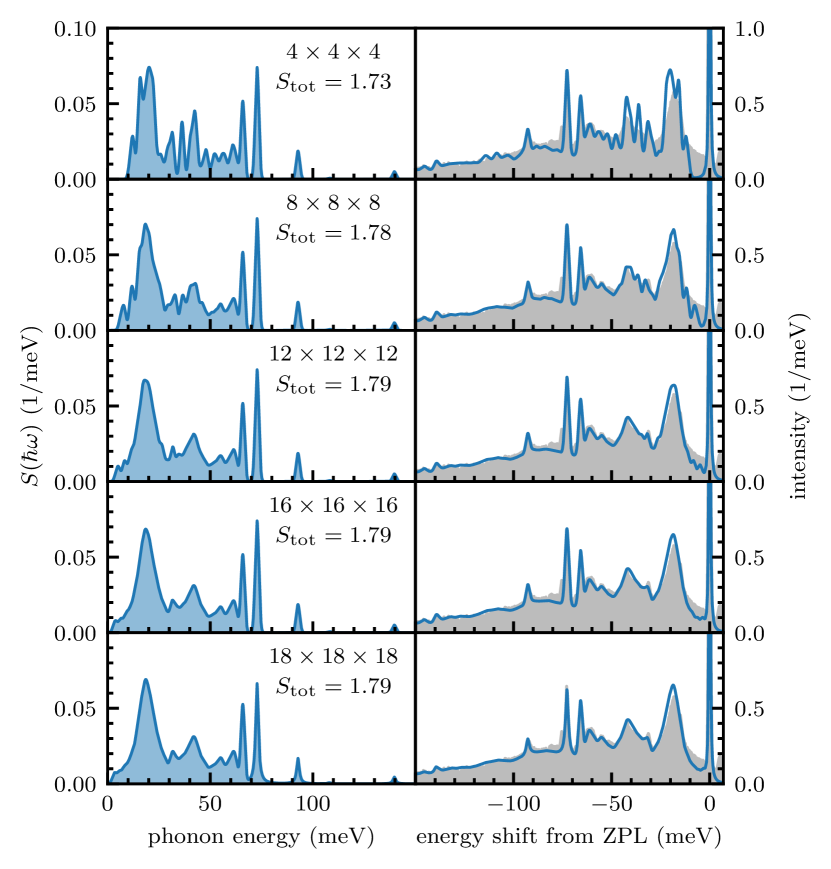
Figure A1 presents the convergence of the spectral density of electron–phonon coupling (left column) and the luminescence lineshapes (right column) as a function of supercell size, ranging from ( atoms) to ( atoms). These calculations were performed using the SCAN functional. The spectral density was computed using Eq. (13), where the -functions for phonon modes below \qty65\milli were approximated by Gaussians with a width of . In contrast, the localized modes above \qty65\milli were modeled using Lorentzians with a HWHM parameter of . Fig. A1 demonstrates that, for the chosen smoothing parameters, the convergence of the spectral function and the optical lineshape is achieved with the supercell, as the difference between the results for the and supercells is minimal.
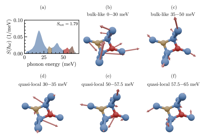
Appendix B Visualization of bulk-like and quasi-local vibrational modes
To illustrate the electron–phonon interaction contributions from the continuum of modes below \qty65\milli, we computed the effective vibrational modes using the following equation:
| (16) |
Here is obtained from Eq. (12), and represents the selected frequency interval encompassing a set of phonons. For example, to represent bulk-like vibrational modes that arise from high phonon density regions, we selected frequency intervals of \qtyrange030\milli and \qtyrange3550\milli. Figure B1(a) displays the spectral density of the electron–phonon coupling, highlighting the chosen frequency regions below \qty65\milli. Figures B1(b) and (c) show the effective vibrational modes localized on defect atoms and their adjacent neighbors, corresponding to bulk-like vibrations. In contrast, Figs. B1(d)–(f) depict quasi-localized vibrational resonances, computed for the frequency ranges \qtyrange3035\milli, \qtyrange5057.5\milli, and \qtyrange57.565\milli, respectively.