Structural and electrical properties of fiber textured and epitaxial molybdenum thin films prepared by magnetron sputter epitaxy
Author Balasubramanian Sundarapandian1,*, Author Mohit Raghuwanshi1, Author Patrik Straňák1, Author Yuan Yu1, Author Haiyan Lyu2, Author Mario Prescher2, Author Lutz Kirste1 Author Oliver Ambacher3
1 Fraunhofer Institute for Applied Solid State Physics, Tullastraße 72, 79108 Freiburg im Breisgau, Germany
2 Institute of Physics (IA), RWTH Aachen University, Sommerfeldstraße 14, 52074 Aachen, Germany
3 Institute for Sustainable Systems Engineering (INATECH), University of Freiburg, Emmy-Noether-Straße 2, University of Freiburg, 79110 Freiburg im Breisgau, Germany
* balasubramanian.sundarapandian@iaf.fraunhofer.de
Abstract
Molybdenum (Mo) due to its optimal structural, physical, and acoustic properties find application as electrode material in aluminum scandium nitride (AlScN) and aluminum nitride (AlN) based bulk acoustic wave (BAW) resonators. Epitaxial Mo thin films exhibiting low resistivity can improve the performance of the BAW resonator by enhancing both the electromechanical coupling coefficient () and quality factor Q. In this study, we systematically vary the growth temperature of Mo grown on fiber-textured and epitaxial wurtzite-aluminum nitride (AlN) to study the changes in structural and electrical properties of the Mo films. Results show that Mo grown at 700°C on epitaxial AlN exhibit low surface roughness ( = 0.8 nm), large average grain diameter ( = 330 nm), low resistivity ( = 6.60.06cm), and high crystal quality (XRD Mo 110 -FWHM = 0.63°). XRD pole figure and -scan analysis reveal that irrespective of the growth temperature, Mo is fiber textured on fiber-textured AlN, and has three rotational domains on epitaxial AlN. The study shows that the resistivity of Mo reduces with increasing growth temperature, which we relate to increasing average grain diameter. Additionally, we show that fiber-textured Mo has more high angle grain boundaries resulting in consistently higher resistivity than its epitaxial equivalent.
The advent of 5G telecommunication standard demands wide bandwidth filters for operation at frequencies ranging between 3.3 GHz and 5.9 GHz with minimal acoustic loss.[2] Bulk acoustic wave (BAW) resonators offer high electro-mechanical coupling coefficient (), high quality factor (Q), and low temperature coefficient of frequency (TCF), making them desirable for the requirements imposed by the telecommunication industry.[36, 26, 1, 27] BAW resonators consist of a piezoelectric material sandwiched between electrodes, material properties of these layers determine the figure of merit (FOM) [Q] of these resonators. Aluminum nitride (AlN) thin films due to their optimal piezoelectric, [33, 47] acoustic, [14] and physical properties [42] were conventionally used as piezoelectric material. After the discovery that aluminum scandium nitride[3] (AlScN) prepared by alloying AlN and scandium nitride (ScN) can provide relatively high intrinsic electro-mechanical coupling coefficient and piezo-electric coefficient ,[53] it is replacing AlN based BAW resonators. BAW resonators employing epitaxial AlN as the piezoelectric material, showed improved power handling capabilities,[50] and .[40] The same is expected for AlScN, therefore a bottom electrode material exhibiting epitaxy is desired to promote epitaxial growth of AlScN. Materials such as platinum (Pt),[15] molybdenum (Mo),[10] iridium (Ir),[12] and tungsten (W) [7] are commonly used as electrodes for AlN based BAW resonators. They have shown to promote AlN growth in the 0001 direction, hence the same is expected for wurtzite-AlScN. Additionally, properties such as acoustic impedance , electrical resistivity , and low mass density determine the performance of the BAW resonators. Large differences in of two media increases the reflection of waves at the interfaces and therefore may increase the energy density leading to an increased in acoustic resonators. Therefore, a large disparity in acoustic impedance of the piezoelectric material and electrode material is desired. Low , and low is particularly crucial to improve Q and reduce mass loading, [45, 23] respectively. Lee et al. have studied the influence of electrode materials such as molybdenum (Mo), aluminum (Al), and tungsten (W) on the resonator properties and found that FOM for Mo based solidly mounted resonator (SMR) to be higher than Al and W based resonators.[25] Ueda et al. showed that Mo, Ru, and W based film bulk acoustic resonators (FBARs) achieved low losses by comparing FBARs with electrode materials such as Al, titanium (Ti), copper (Cu), gold (Au), chromium (Cr), Mo, ruthenium (Ru), and W.[48] Since, Mo was found to have optimal structural, physical, and acoustic properties, it has emerged as the choice of electrode material for BAW resonators. To promote oriented growth of Mo on Si substrates, other groups have used AlN as a seed layer,[21, 19, 10] therefore a similar approach was taken in this work. Additionally, the thermal expansion coefficient of Mo is similar to AlN, [56, 18] making AlN an ideal seed layer for Mo growth. In this work, we systematically vary the growth temperature and demonstrate the change in structural and electrical properties of Mo thin films, sputtered on fiber-textured and epitaxial AlN thin films prepared by magnetron sputter epitaxy.
AlN and Mo films were prepared using an Evatec Clusterline 200II planar magnetron sputtering module with a leak rate of 7.510-7 mbar l/s. Both the films were deposited at a working pressure of 110-3 mbar. Al, and Mo targets (304 mm diameter) were used to deposit AlN, and Mo films onto 200 mm Si(111) substrates. The native oxide layer that grows unintentionally on the silicon substrate was cleaned using in-situ inductively coupled plasma (ICP) etching. All the substrates were etched with an MF power of 500 W, RF power of 50 W, at 510-6 mbar Ar pressure for 85 s. More information about thickness of native oxide and its evolution after ICP etching can be found in our previous work.[51] AlN was sputtered at 500 °C, and 700 °C to obtain fiber-textured and epitaxial films, respectively.[44] Process parameters such as power, gas flow, and target to substrate distance (TSD) were kept constant at 5500 W, 40 sccm, and 10 mm respectively. Mo thin films were sputtered on AlN thin films at growth temperatures between 300 °C and 700 °C in steps of 100 °C, while keeping the power, gas flow, and TSD constant at 1000 W, 25 sccm, and 60 mm, respectively. Surface morphology, surface roughness (), and average grain diameter () of the films were characterized using Bruker ICON AFM. An IONTOF M6 Plus time-of-flight secondary ion mass spectrometer (TOF-SIMS) was used to determine the thickness of the films, and interface diffusion. A PANalytical X’Pert Pro MRD diffractometer with a Ge-220 hybrid monochromator providing Cu-K was used to perform X-ray diffraction (XRD) and X-ray reflectivity (XRR) analysis. Electrical resistivity () of the films were determined at the center of the wafer using four point probe method. To account for the error, each sample was measured five times at approximately the same position. EBSD measurements were carried out using an EDAX-Hikari camera mounted on the FEI Helios NanoLab 650. EBSD analyses were performed under SEM conditions at 20 kV and 1.6 nA. Data acquisition utilized a 22 bin-ning resolution and the subsequent data processing was completed using OIM analysis software, which identified properties of GBs based on the detected Kikuchi patterns.
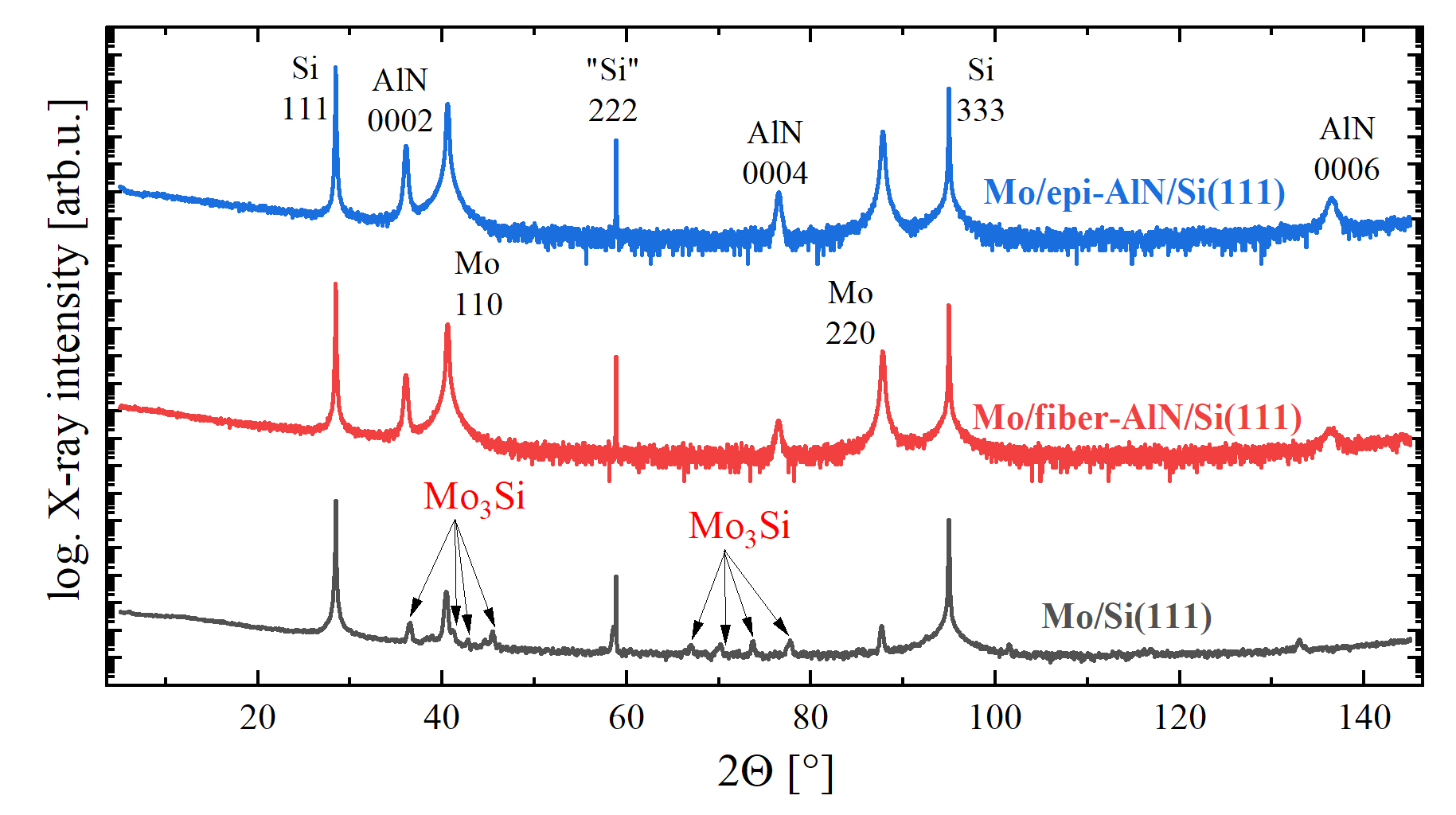
XRD scans performed on Mo deposited at 700°C on Si(111), fiber-textured, and epitaxial AlN are shown in figure 1. The scans demonstrate absence of peaks corresponding to molybdenum silicides (Mo3Si) when body-centered cubic (bcc) Mo was sputtered on fiber-textured and epitaxial AlN. This result emphasizes the importance of the use of AlN as a seed layer for Mo growth on silicon substrates. Peaks from Mo3Si were also absent when Mo was sputtered at growth temperatures below 700°C (see figure S1 in supplementary material). Additionally, ToF-SIMS measurement showed that there is slight diffusion of Mo, and Si into the AlN layer (see figure S5 in supplementary), indicating that a certain thickness of AlN layer is required to prevent formation of Mo3Si. The thickness of the films (see table S1), as determined using ToF-SIMS measurements remained constant for all growth temperatures at 120 nm, and hence the growth rate at 1.04 nm/s. Crystal orientations that can be observed for Mo deposited on AlN depends on the polarity of AlN. When bcc-Mo is deposited on N-Polar AlN, Mo is expected to grow with both (110) and (100) planes parallel to the AlN (0001) basal plane, while on metal polar AlN only Mo (110) plane is expected.[16] For Mo deposited on fiber-textured and epitaxial AlN, reflections from AlN 000l (l = 2,4,6), Mo 110 and Mo 220 were observed. This shows that Mo grows with its (110) plane parallel to the AlN (0001) basal plane. In our previous work, we have shown that our AlN is mixed polar[44, 43] which could be the reason for the absence of Mo 200 reflection. Moreover, analysis of a similar stack deposited on sapphire showed reflection from (200) plane.[54] Since (110) planes of Mo are densely packed, they are expected to have minimum surface, and interface energies, promoting (110) plane parallel to the substrate.[46] Given the preference, the (100) planes that are expected to grow on N-polar domains maybe are suppressed, leading to the absence of (100) planes parallel to the substrate.
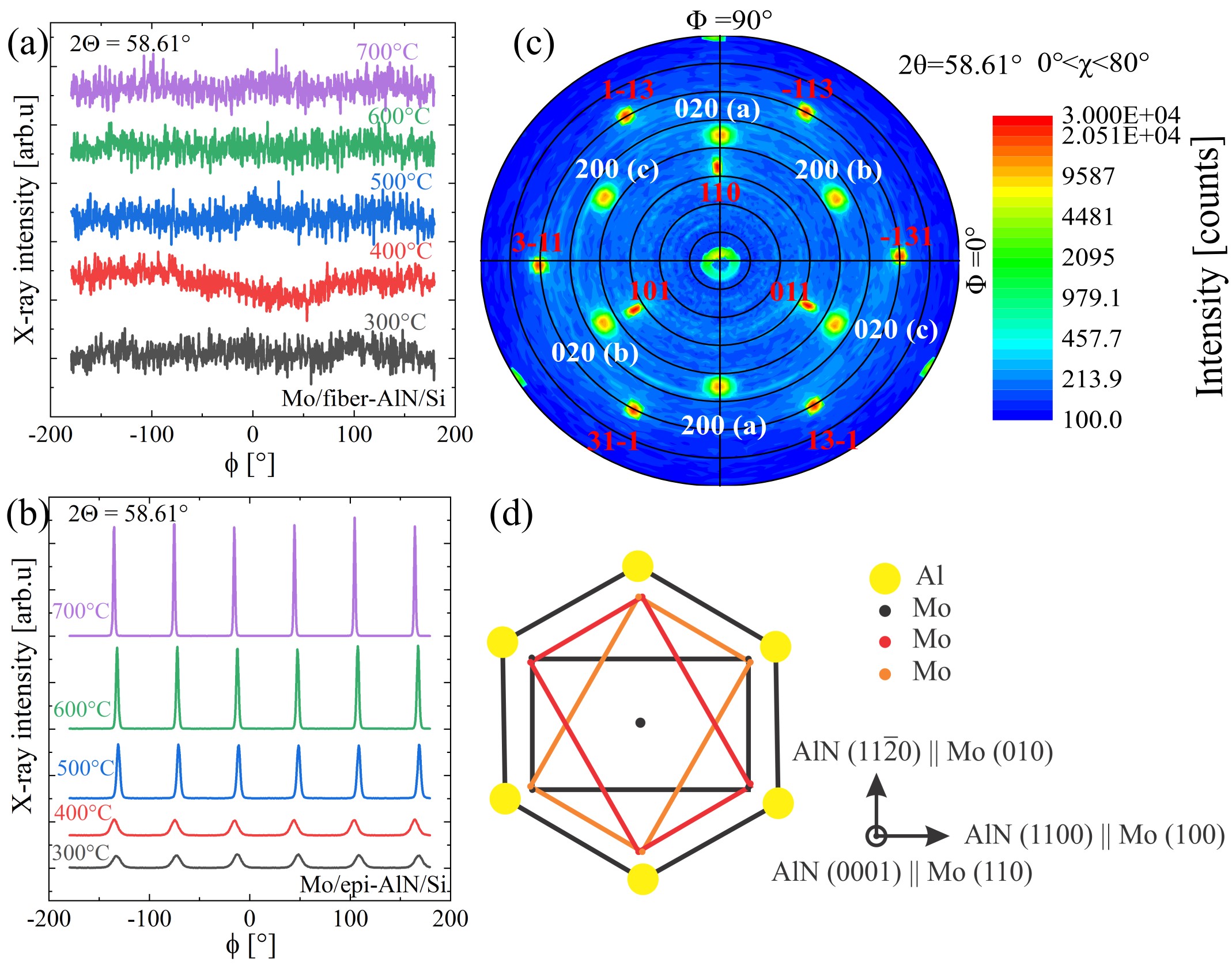
-scan, and pole figure (PF) shown in figure 2 were recorded for Mo 200 reflection at 58.61°. Irrespective of the growth temperature, Mo deposited on fiber-textured AlN showed no peaks in -scan indicating that Mo is fiber-textured [20] (see figure 2 (a)). On epitaxial AlN, at all growth temperatures -scan recorded from Mo 200 reflection showed six peaks separated by 60°, indicating that Mo has an orientational relationship (OR) with AlN (see figure 2(b)). This result also shows that the texture of Mo is independent of the growth temperature, and is dictated predominantly by the crystallographic texture of AlN seed layer. Distribution of grain misorientation determined using EBSD (see figure S4 in supplementary material) showed that the grains prefer to grow with a misorientation angle of 60° irrespective of the crystallographic texture, as this orientation has been observed to have the least grain boundary energy in bcc metals.[11] Even though there is a preferred orientation for the grains, it is possible that the interface energy anisotropy for grain rotation in case of epitaxial AlN is high, constraining Mo grains to grow in a specific orientation.[46] PF recorded between angles of 0° and 80° is shown in figure 2 (c), reflections marked in red correspond to silicon while the ones marked in white correspond to Mo. At 45°, six reflections can be observed, matching the number of reflections seen in the -scans. Stereographic projections simulated for Mo oriented along the [110] direction showed only two reflections corresponding to (100) and (010) planes at = 45°. The presence of additional four reflection in the PF indicates the presence of additional two domains of Mo which was also observed in EBSD maps (see figure s3 in supplementary material). The reflections from these three domains are marked with letters a, b, and c in figure 2 (c). Similar conclusions were made for bcchcp systems.[30, 17, 54] The three domains of Mo(110) on AlN(0001) basal plane is schematically shown in figure 2 (d), the three domains are marked in black, red, and orange. The OR of the three domains were determined to be AlN[110]Mo[010], AlN[110]Mo[010] and AlN[110]Mo[010]. Since Mo on fiber-textured AlN is fiber-textured, and has an OR with epitaxial AlN, they will be called “Fiber-Mo” and “Epi-Mo”, respectively in the rest of the text. At the measured 2 angle, reflections from Si{113} and Si{110} were observed at 60° and 35° respectively. These reflections are marked red in figure 2 (c). Table 1 compares present study’s findings with previously reported XRD rocking curve full width at half maximum (-FWHM) of Mo 110 reflection sputtered on Si with an AlN seed layer. The table clearly demonstrates that the crystalline properties of Mo reported in this work is superior to the previously reported values. Based on the information available in the papers, and given that we obtain Mo with high crystalline quality on both fiber textured and epitaxial AlN at 700°C, we believe that growth temperature is a key factor in obtaining Mo with high crystalline quality on AlN.
|
|
Texture | ||||||
|---|---|---|---|---|---|---|---|---|
| J.S. Cherng et al.[10] | 25/1500 | 1.9 |
|
|||||
| R.E.Sah et al.[39] | 600/170 | 6 |
|
|||||
| Toshihiro et al.[20] | 100/200 | 4 |
|
|||||
|
85/116 | 0.78 |
|
|||||
|
97/116 | 0.63 |
|
The surface morphology of Mo deposited at growth temperatures of 300°C, 500°C, and 700°C on fiber-textured and epitaxial AlN is shown in figure 3. Mo on fiber-textured AlN is shown in panels (a) - (c), while panels (d) - (f) show Mo grown on epitaxial AlN. As a consequence of the increase in adatom diffusion with temperature, an increase in grain diameter was observed in both fiber and epi-Mo. The average grain diameter () determined from the AFM images is shown in figure 4 (a), in both the cases increased with growth temperature. The surface diffusion coefficient D can be expressed as ,[37] the exponential increase in D with growth temperature could be the reason for the increase in . For Epi-Mo, the increased from 38 nm at 300°C to 330 nm at 700°C, while for fiber-textured Mo increased from 32 nm to 207 nm. Above 500°C, the rate of increase in is less pronounced for fiber-textured Mo, indicating that the texture of Mo has an influence on the surface diffusion of ad-atoms. Since Mo is fiber-textured, the random orientation of Mo grains could act as an additional barrier for Mo adatoms to diffuse between grains, thereby limiting the .
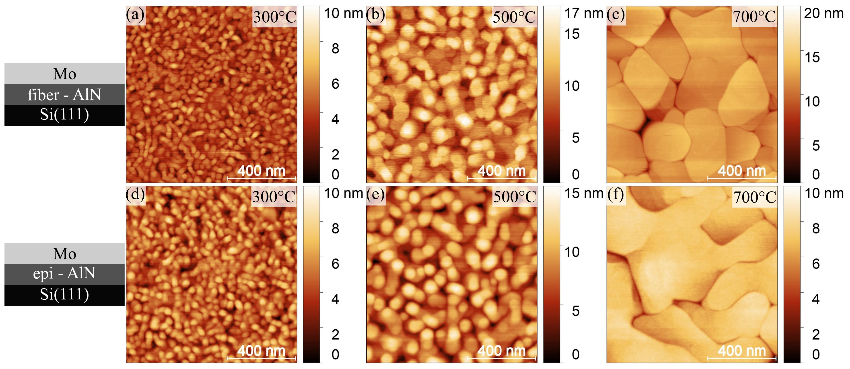
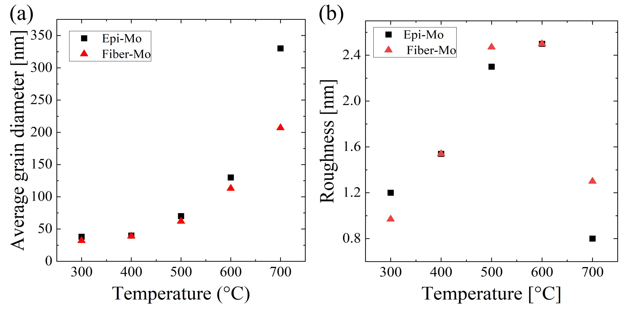
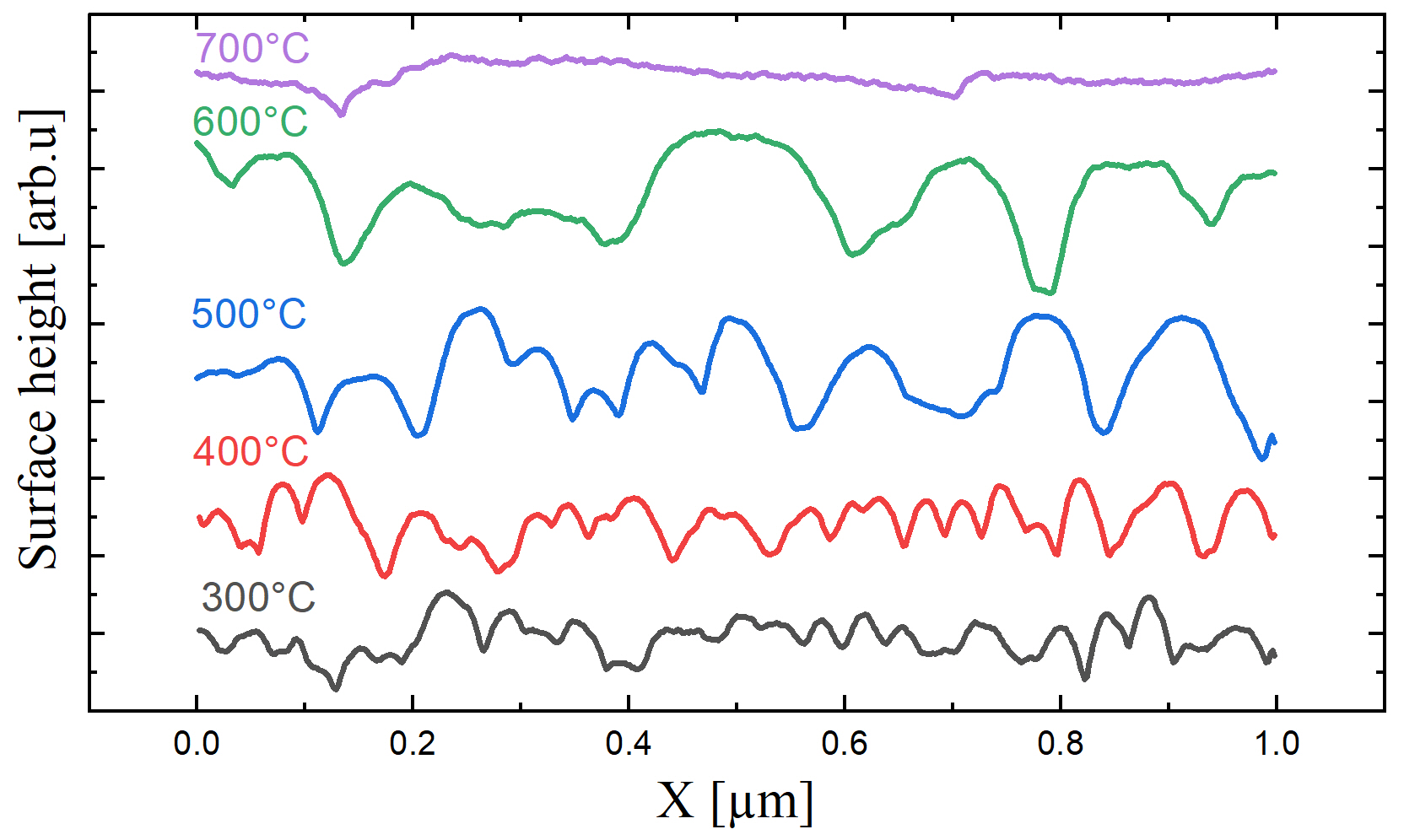
The change in surface roughness () as a function of growth temperature determined as root mean square (RMS) of the surface height for epitaxial and fiber-textured Mo is depicted in figure 4(b). Interestingly, reached a maximum at 600°C, for both the cases. XRR recorded for these samples showed that the rate of decay of reflections which is roughness dependent,[31] followed a similar trend (see figure S2 in supplementary file). Additionally, the mass density of the films extracted by fitting the reflections remained constant at 10.2 g/cm3, indicating that the density of Mo is independent of growth temperature, and crystallographic texture. For fiber-textured and epitaxial Mo, dropped to 1.3 nm and 0.8 nm, respectively at 700°C. Surface profiles extracted from AFM images of epitaxial Mo deposited at different growth temperatures is shown in figure 5. With increasing growth temperature, a change in shape of the grains can be observed. At growth temperatures of 300°C, and 400°C the surface of the grains predominantly have an inverted V-shape. The inverted V-shape is a result of anisotropy in growth rate of different crystallographic planes, the facets of the inverted V corresponds to crystallographic planes with low growth rates. As growth temperature increases, surface diffusion of ad-atoms between grains happen resulting in grain growth. At 600°C, the grains start to flatten, and at 700°C almost no inverted V shaped grains can be observed. This could be due to recrystallization resulting in the observed drop in . Since 600°C, corresponds to a / ratio of 0.3, recrystallization can be expected at this temperature.[41] Here, is the melting point of Mo, and it was assumed to be 2895 K [55], and is the substrate temperature.
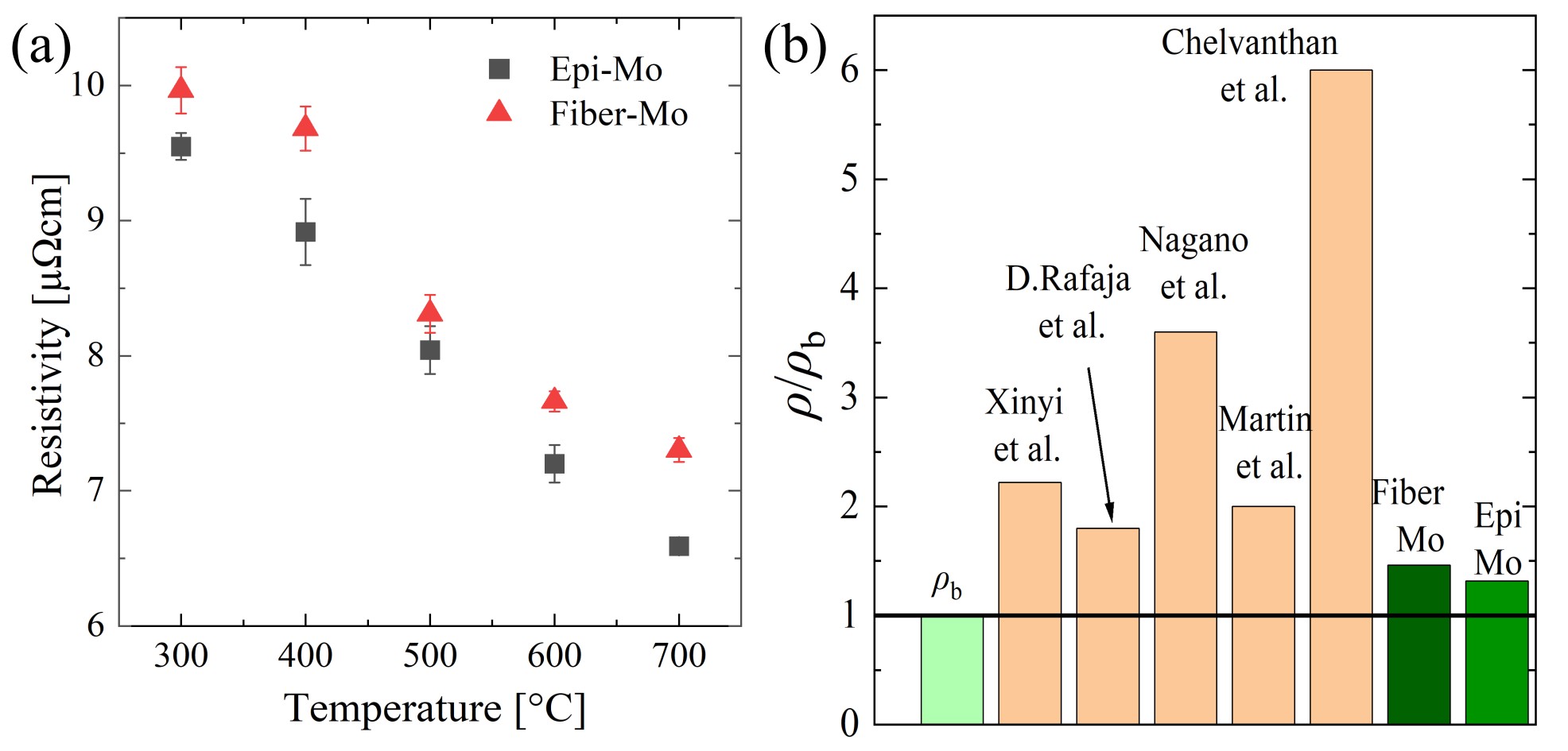
Electrical resistivity () of epi, and fiber Mo determined using four point probe method is shown in figure 6 (a). of both epi, and fiber Mo decreased with increasing growth temperature. of thin films depends on the thickness of the films, grain boundary scattering, scattering due to macroscopic roughness, and impurities in thin films. is expected to decrease with increasing thickness, due to scattering of electrons at the film surface. Since the thickness of the Mo films investigated were approximately the same, it is not contributing to the observed decrease in . Increase in roughness of the films is expected to increase the .[34] Though roughness of both fiber-textured and epitaxial Mo increase up to a growth temperature of 600°C, a decrease in can be observed. This shows that the contribution to by roughness, even if present is not the dominant effect. Oxygen concentration in Mo films can also affect its , [4] ToF-SIMS measurement revealed that the Mo thin films have approximately the same level of oxygen irrespective of its crystallographic texture, and growth temperature (see Figure S6). Therefore, oxygen concentration in the films have a negligible effect on the observed change in . Grain boundaries can act as planes that partially reflect electrons,[29] thereby increasing of the films. With increasing , grain boundary density reduces and hence its . In figure 4 (a) it was shown that increases with temperature, which could be the reason for the decreasing with temperature. Figure 6 (b), compares the resistivity of fiber Mo and epi Mo obtained in this work with work of other researchers. Here, the resistivity is normalized to bulk resistivity of Mo . was assumed to be 5.5cm.[52] From the figure, it can be seen that the resistivity of Mo obtained in this work is close to and better than other works. [13, 38, 28, 9, 32]
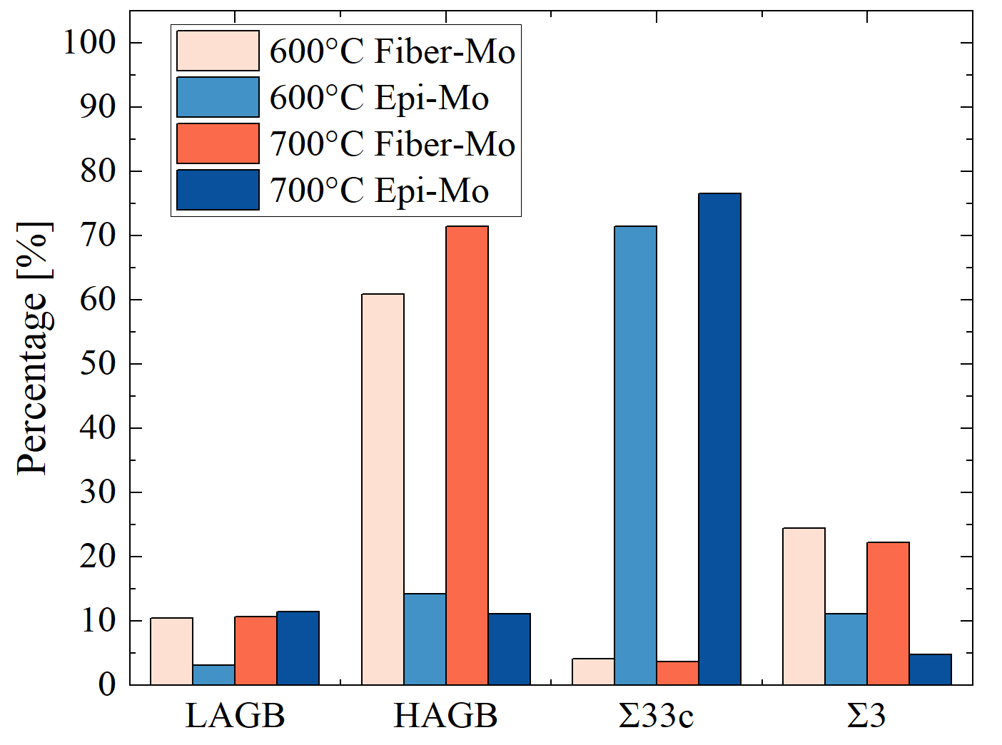
At growth temperatures below 600°C, where the of both epitaxial and fiber-textured Mo is approximately the same, epitaxial Mo showed consistently lower than fiber-textured Mo (see figure 6 (a)). This indicates that there is an additional effect contributing to the of the films. In addition to grain diameter, the type of grain boundary i.e whether the grain boundary is a low-angle grain boundary(LAGB), high-angle grain boundary (HAGB), or a sigma () boundary influences the scattering of electrons at the grain boundary.[5, 6, 8, 24, 57] Therefore, the grain boundaries present in Mo films grown at 600°C and 700°C on fiber-textured and epitaxial AlN were characterized using EBSD. The analysis showed that all the films contained LAGBs, HAGBs, 33c, and 3 grain boundaries, the percentage distribution of these boundaries in the films is shown in figure 7. The results clearly show that Mo grown on epitaxial AlN has more boundaries than fiber-textured Mo, while fiber-textured Mo has significantly more HAGB than epitaxial Mo. In Mo, HAGB are more resistive than LAGB, [22] and since boundaries have high symmetry one could expect low scattering of electrons at these boundaries than HAGB. Therefore, it can be concluded that the grain boundaries in fiber-textured Mo scatters more electrons than epitaxial Mo, resulting in higher at growth temperatures below 600°C. Furthermore, an increase in grain boundary density increases the impurities concentrated at the grain boundaries. This in turn increases the potential barrier for mobile electrons to move from one grain to another, localizing electrons in their own grains,[49, 35] increasing of the films. A systematic study is required to characterize the impurities at the grain boundaries to further comment on this.
In summary, our results show that the growth temperature of Mo has significant effects on the, crystal quality, average grain diameter, roughness, and electrical resistivity of the films. Through XRD -scan, and pole figure analysis we show that the crystallographic texture of Mo sputtered on AlN thin films, is dictated by the texture of the AlN film, independent of growth temperature. Irrespective of the crystallographic texture of Mo, the average grain diameter increases with growth temperature due to increased mobility of ad-atoms. The roughness of the films reach a maximum at a growth temperature of 600°C, and drops significantly at 700°C, due to re-crystallization of Mo. The resistivity of the films decrease with increasing growth temperature, as a consequence of increasing grain diameter, reaching a minimum of 6.60.06cm at 700°C for Mo grown on epitaxial AlN. Fiber-textured Mo has more high angle grain boundaries than epitaxial Mo, leading to increased resistivity of these films. Our results show that Mo grown at 700°C on epitaxial AlN has favourable properties for use as electrode material in AlScN and AlN based BAW resonators.
Supplementary material
See supplementary material for XRD- scans of Mo sputtered at various temperatures on fiber textured and epitaxial AlN (Figure S1), XRR scans recorded for fiber textured and epitaxial Mo(Figure S2), exemplary EBSD map of fiber-Mo and epi-Mo (Figure S3), distribution of grain misorientation in fiber-Mo, and epi-Mo (Figure S4), ToF-SIMS measurement of fiber-Mo and epi-Mo sputtered at 300°C, 500°C, and 700°C (Figure S5), and the approximate thickness of the AlN and Mo layers determined using ToF-SIMS (Table S1). ToF-SIMS measurements of oxygen levels in Mo sputtered at 300°C, 500°C, and 700°C on fiber textured and epitaxial AlN (Figure S6).
Acknowledgements
This project was performed within the framework of COMET—Competence Centers for Excellent Technologies and ASSIC Austrian Smart Systems Integration Research Center, which is funded by BMVIT, BMDW, and the Austrian provinces of Carinthia and Styria. The COMET programme is run by FFG. The authors would also like to thank Nadine Brückner for XRD measurements. Dr.Jürgen weippert, Dr.Maximilian Kessel, and Dr. Bernd Heinz for their help with the sputter tool, and fruitful discussions.
Conflict of Interest
The authors have no conflicts to disclose.
Data availability
The data that support the findings of this study are available from the corresponding author upon reasonable request.
References
- 1. R. Aigner. SAW and BAW technologies for RF filter applications: A review of the relative strengths and weaknesses. In 2008 IEEE Ultrasonics Symposium, pages 582–589. IEEE, 2008.
- 2. R. Aigner, G. Fattinger, M. Schaefer, K. Karnati, R. Rothemund, and F. Dumont. BAW filters for 5G bands. In 2018 IEEE International Electron Devices Meeting (IEDM), pages 14–5. IEEE, 2018.
- 3. M. Akiyama, T. Kamohara, K. Kano, A. Teshigahara, Y. Takeuchi, and N. Kawahara. Enhancement of piezoelectric response in scandium aluminum nitride alloy thin films prepared by dual reactive cosputtering. Advanced Materials, 21(5):593–596, 2009.
- 4. T. Bardin, J. Pronkoz, R. Budhani, J. Lin, and R. Bunshah. The effects of oxygen concentration in sputter-deposited molybdenum films. Thin solid films, 165(1):243–247, 1988.
- 5. H. Bishara, M. Ghidelli, and G. Dehm. Approaches to measure the resistivity of grain boundaries in metals with high sensitivity and spatial resolution: A case study employing Cu. ACS Applied Electronic Materials, 2(7):2049–2056, 2020.
- 6. H. Bishara, S. Lee, T. Brink, M. Ghidelli, and G. Dehm. Understanding grain boundary electrical resistivity in Cu: The effect of boundary structure. ACS nano, 15(10):16607–16615, 2021.
- 7. P. Bradley, J. Kim, S. Ye, P. Nikkel, S. Bader, and C. Feng. 12E-0 2X size and cost reduction of film bulk acoustic resonator (FBAR) chips with tungsten electrodes for PCS/GPS/800 MHz multiplexers. In 2007 IEEE Ultrasonics Symposium Proceedings, pages 1144–1147. IEEE, 2007.
- 8. M. César, D. Liu, D. Gall, and H. Guo. Calculated resistances of single grain boundaries in copper. Physical Review Applied, 2(4):044007, 2014.
- 9. P. Chelvanathan, Z. Zakaria, Y. Yusoff, M. Akhtaruzzaman, M. Alam, M. Alghoul, K. Sopian, and N. Amin. Annealing effect in structural and electrical properties of sputtered Mo thin film. Applied Surface Science, 334:129–137, 2015.
- 10. J. Cherng, T. Chen, and C. Lin. Pulsed-DC sputtering of molybdenum bottom electrode and piezoelectric aluminum nitride films for bulk acoustic resonator applications. Thin Solid Films, 519(20):6797–6800, 2011.
- 11. O. Chirayutthanasak, R. Sarochawikasit, S. Khongpia, T. Okita, S. Dangtip, G. S. Rohrer, and S. Ratanaphan. Universal function for grain boundary energies in bcc metals. Scripta Materialia, 240:115821, 2024.
- 12. M. Clement, J. Olivares, E. Iborra, S. González-Castilla, N. Rimmer, and A. Rastogi. AlN films sputtered on iridium electrodes for bulk acoustic wave resonators. Thin Solid Films, 517(16):4673–4678, 2009.
- 13. X. Dai, A. Zhou, L. Feng, Y. Wang, J. Xu, and J. Li. Molybdenum thin films with low resistivity and superior adhesion deposited by radio-frequency magnetron sputtering at elevated temperature. Thin Solid Films, 567:64–71, 2014.
- 14. M.-A. Dubois and P. Muralt. Properties of aluminum nitride thin films for piezoelectric transducers and microwave filter applications. Applied Physics Letters, 74(20):3032–3034, 1999.
- 15. M.-A. Dubois, P. Muralt, and V. Plessky. BAW resonators based on aluminum nitride thin films. In 1999 IEEE Ultrasonics Symposium. Proceedings. International Symposium (Cat. No. 99CH37027), volume 2, pages 907–910. IEEE, 1999.
- 16. C. Gao, O. Brandt, S. C. Erwin, J. Lähnemann, U. Jahn, B. Jenichen, and H.-P. Schönherr. “Cube-on-hexagon” orientation relationship for Fe on GaN(000): The missing link in bcc/hcp epitaxy. Physical Review B, 82(12):125415, 2010.
- 17. C. Gao, O. Brandt, H.-P. Schönherr, U. Jahn, J. Herfort, and B. Jenichen. Thermal stability of epitaxial Fe films on GaN(0001). Applied Physics Letters, 95(11):111906, 2009.
- 18. P. Hidnert and W. Gero. Thermal expansion of molybdenum. Number 488. US Department of Commerce, Bureau of Standards, 1924.
- 19. T. Kamohara, M. Akiyama, and N. Kuwano. Influence of molybdenum bottom electrodes on crystal growth of aluminum nitride thin films. Journal of crystal growth, 310(2):345–350, 2008.
- 20. T. Kamohara, M. Akiyama, N. Ueno, and N. Kuwano. Improvement in crystal orientation of AlN thin films prepared on Mo electrodes using AlN interlayers. Ceramics international, 34(4):985–989, 2008.
- 21. T. Kamohara, M. Akiyama, N. Ueno, K. Nonaka, and H. Tateyama. Growth of highly c-axis-oriented aluminum nitride thin films on molybdenum electrodes using aluminum nitride interlayers. Journal of crystal growth, 275(3-4):383–388, 2005.
- 22. A. Karolik and A. Luhvich. Calculation of electrical resistivity produced by dislocations and grain boundaries in metals. Journal of Physics: Condensed Matter, 6(4):873, 1994.
- 23. M. Knapp, R. Hoffmann, V. Lebedev, V. Cimalla, and O. Ambacher. Graphene as an active virtually massless top electrode for RF solidly mounted bulk acoustic wave (SMR-BAW) resonators. Nanotechnology, 29(10):105302, 2018.
- 24. J. Lee, M. Lamarche, and V. P. Georgiev. The first-priniple simulation study on the specific grain boundary resistivity in copper interconnects. In 2018 IEEE 13th Nanotechnology Materials and Devices Conference (NMDC), pages 1–4. IEEE, 2018.
- 25. S.-H. Lee, K. H. Yoon, and J.-K. Lee. Influence of electrode configurations on the quality factor and piezoelectric coupling constant of solidly mounted bulk acoustic wave resonators. Journal of Applied Physics, 92(7):4062–4069, 2002.
- 26. S. Mahon. The 5G effect on RF filter technologies. IEEE Transactions on Semiconductor Manufacturing, 30(4):494–499, 2017.
- 27. D. Malocha. SAW/BAW acoustoelectronic technology for filters and communication systems. In 2010 IEEE 11th Annual Wireless and Microwave Technology Conference (WAMICON), pages 1–7. IEEE, 2010.
- 28. F. Martin, P. Muralt, and M.-A. Dubois. Process optimization for the sputter deposition of molybdenum thin films as electrode for AlN thin films. Journal of Vacuum Science & Technology A, 24(4):946–952, 2006.
- 29. A. Mayadas and M. Shatzkes. Electrical-resistivity model for polycrystalline films: the case of arbitrary reflection at external surfaces. Physical review B, 1(4):1382, 1970.
- 30. R. Meijers, R. Calarco, N. Kaluza, H. Hardtdegen, M. Ahe, H. Bay, H. Lüth, M. Buchmeier, and D. Bürgler. Epitaxial growth and characterization of Fe thin films on wurtzite GaN(0001). Journal of crystal growth, 283(3-4):500–507, 2005.
- 31. M. Moram and M. Vickers. X-ray diffraction of III-nitrides. Reports on progress in physics, 72(3):036502, 2009.
- 32. J. Nagano. Electrical resistivity of sputtered molybdenum films. Thin Solid Films, 67(1):1–8, 1980.
- 33. R. S. Naik, J. J. Lutsky, R. Reif, C. G. Sodini, A. Becker, L. Fetter, H. Huggins, R. Miller, J. Pastalan, G. Rittenhouse, and Y. Wong. Measurements of the bulk, c-axis electromechanical coupling constant as a function of AlN film quality. IEEE transactions on ultrasonics, ferroelectrics, and frequency control, 47(1):292–296, 2000.
- 34. Y. Namba. Resistivity and temperature coefficient of thin metal films with rough surface. Japanese Journal of Applied Physics, 9(11):1326, 1970.
- 35. V. H. Nguyen, U. Gottlieb, A. Valla, D. Muñoz, D. Bellet, and D. Muñoz-Rojas. Electron tunneling through grain boundaries in transparent conductive oxides and implications for electrical conductivity: the case of ZnO: Al thin films. Materials Horizons, 5(4):715–726, 2018.
- 36. T. Nishihara, T. Yokoyama, T. Miyashita, and Y. Satoh. High performance and miniature thin film bulk acoustic wave filters for 5 GHz. In 2002 IEEE Ultrasonics Symposium, 2002. Proceedings., volume 1, pages 969–972. IEEE, 2002.
- 37. M. Ohring. Materials Science of Thin Films: Depositon and Structure. Elsevier, 2001.
- 38. D. Rafaja, H. Köstenbauer, U. Mühle, C. Löffler, G. Schreiber, M. Kathrein, and J. Winkler. Effect of the deposition process and substrate temperature on the microstructure defects and electrical conductivity of molybdenum thin films. Thin Solid Films, 528:42–48, 2013.
- 39. R. Sah, L. Kirste, H. Kirmse, M. Mildner, L. Wilde, S. Kopta, F. Knöbber, M. Krieg, V. Cimalla, V. Lebedev, and O. Ambacher. Crystallographic texture of submicron thin aluminum nitride films on molybdenum electrode for suspended micro and nanosystems. ECS Journal of Solid State Science and Technology, 2(4):P180, 2013.
- 40. J. B. Shealy, J. B. Shealy, P. Patel, M. D. Hodge, R. Vetury, and J. R. Shealy. Single crystal aluminum nitride film bulk acoustic resonators. In 2016 IEEE Radio and Wireless Symposium (RWS), pages 16–19. IEEE, 2016.
- 41. P. G. Shewmon. Transformations in metals. McGraw-Hill, 1969.
- 42. G. A. Slack, R. A. Tanzilli, R. Pohl, and J. Vandersande. The intrinsic thermal conductivity of AlN. Journal of Physics and Chemistry of Solids, 48(7):641–647, 1987.
- 43. B. Sundarapandian, D. Q. Tran, L. Kirste, P. Straňák, A. Graff, M. Prescher, A. Nair, M. Raghuwanshi, V. Darakchieva, P. P. Paskov, and O. Ambacher. Comparison of aluminum nitride thin films prepared by magnetron sputter epitaxy in nitrogen and ammonia atmosphere. Applied Physics Letters, 124(18), 2024.
- 44. B. Sundarapandian, A. Yassine, L. Kirste, M. Baeumler, P. Straňák, E. Fisslthaler, M. Prescher, M. Yassine, A. Nair, M. Raghuwanshi, and O. Ambacher. Influence of growth temperature on the properties of aluminum nitride thin films prepared by magnetron sputter epitaxy. Journal of Applied Physics, 134(18), 2023.
- 45. R. Thalhammer, G. Fattinger, M. Handtmann, and S. Marksteiner. Ohmic effects in BAW-resonators. In 2006 IEEE MTT-S International Microwave Symposium Digest, pages 390–393. IEEE, 2006.
- 46. C. V. Thompson. Grain growth in thin films. Annual review of materials science, 20(1):245–268, 1990.
- 47. K. Tonisch, V. Cimalla, C. Foerster, H. Romanus, O. Ambacher, and D. Dontsov. Piezoelectric properties of polycrystalline AlN thin films for MEMS application. Sensors and Actuators A: Physical, 132(2):658–663, 2006.
- 48. M. Ueda, T. Nishihara, S. Taniguchi, T. Yokoyama, J. Tsutsumi, M. Iwaki, and Y. Satoh. Film bulk acoustic resonator using high-acoustic-impedance electrodes. Japanese Journal of Applied Physics, 46(7S):4642, 2007.
- 49. J. Vancea and H. Hoffmann. Reduced density of effective electrons in metal films. Thin Solid Films, 92(3):219–225, 1982.
- 50. R. Vetury, M. D. Hodge, and J. B. Shealy. High power, wideband single crystal XBAW technology for sub-6 GHz micro RF filter applications. In 2018 IEEE International Ultrasonics Symposium (IUS), pages 206–212. IEEE, 2018.
- 51. J. Weippert, L. Kirste, P. Straňák, B. Sundarapandian, J. Engels, S. Oeser, A. Graff, and V. Lebedev. Formation of 111 oriented domains during the sputtering epitaxy growth of (001) oriented Iridium films. Journal of Physics: Condensed Matter, 36(40):405001, 2024.
- 52. G. K. White and S. Woods. Electrical and thermal resistivity of the transition elements at low temperatures. Philosophical Transactions of the Royal Society of London. Series A, Mathematical and Physical Sciences, 251(995):273–302, 1959.
- 53. G. Wingqvist, F. Tasnadi, A. Zukauskaite, J. Birch, H. Arwin, and L. Hultman. Increased electromechanical coupling in w-ScxAl1-xN. Applied Physics Letters, 97(11), 2010.
- 54. N. Wolff, S. Fichtner, B. Haas, M. R. Islam, F. Niekiel, M. Kessel, O. Ambacher, C. Koch, B. Wagner, F. Lofink, and L. Kienle. Atomic scale confirmation of ferroelectric polarization inversion in wurtzite-type AlScN. Journal of Applied Physics, 129(3):034103, 2021.
- 55. A. Worthing. The temperature scale and the melting point of molybdenum. Physical Review, 25(6):846, 1925.
- 56. W. Yim and R. Paff. Thermal expansion of AlN, sapphire, and silicon. Journal of Applied Physics, 45(3):1456–1457, 1974.
- 57. T. Zhou, A. Jog, and D. Gall. First-principles prediction of electron grain boundary scattering in fcc metals. Applied Physics Letters, 120(24), 2022.