Wavefront dislocations in graphene systems revealed by transport measurement
Abstract
The wavefront dislocation is an important and ubiquitous phenomenon in wave fields. It is closely related to the phase singularity in a wave function. Some recent studies have verified that the wavefront dislocations in the local density of states (LDOS) map can well manifest the intrinsic topological characteristics in graphene and some topological systems. Different from these previous schemes, we raise a transport method to measure such wavefront dislocations in monolayer and Bernal-stacked bilayer graphene. Combining analytical analysis and numerical calculation, we find phase singularities naturally appear in the transmission coefficients between different sublattices, due to the intervalley interference on the electron propagating paths. These phase singularities could contribute wavefront dislocations in the conductance map. Additionally, in bilayer graphene, the wavefront dislocations are found to remain robust even though the tip is coupled to multiple sublattices. Biased bilayer graphene is also explored. Our scheme provides a new transport routine to explore valley-related topological properties of materials.
I Introduction
In a wavefield, some additional wavefronts (i.e. surface of constant phase) may appear in a certain area associated with a topological defect, which are known as wavefront dislocations. Following the pioneering work of Nye and Berry in [1], this fundamental and ubiquitous phenomenon can in principle emerge in any wavefield irrespectively of its physical nature or its dispersion relation. In mathematics, it originates from a phase indetermination in which the amplitude of wave vanishes. One example is about Aharonov-Bohm effect [2, 3], where the electron wave could possess wavefront dislocations on the flux line of the impenetrable cylinder with a magnetic flux. Since the phase singularities are recognized as important features of all waves, the researches on wavefront dislocations have spread over various domains of physics, from astronomy [4], oceanic tides [5], sounds [1, 6, 7], to optics [8, 9] and fluids [2, 5, 10]. Especially in optics, it gives birth to a new research branch known as singular optics [11, 12].
Due to wave-particle duality, electrons can also be regarded as waves. In the field of condensed matter physics, it is recently found that wavefront dislocations could closely link the topological defect of waves with the topological properties of materials. This topology is associated with some topological indices, which are featured by the phase singularities of bulk electron wave functions [13, 14, 15, 16, 17]. Thus, through measuring wavefront dislocations originated from the phase singularity, the topological properties of this system can be manifested. For example, in monolayer and bilayer graphene [18, 19, 20], by introducing a single atom vacancy or a hydrogen atom chemisorbed on a carbon site, dislocations in charge density modulations (i.e. Friedel oscillations [21]) induced by intervalley scatterings can be observed in the scanning tunneling microscopy (STM). The number of wavefront dislocations characterizes the (local) Berry phase signatures. In 1D SSH chain [22, 23], the wavefront dislocations in the local density of states (LDOS) map of standing wave pattern could present a direct evidence of bulk topological transition.
The LDOS fluctuations are attributed to the quantum interference between the incident and scattering wave induced by a defect or boundary in the material [24, 25, 26]. If the incident wave function and scattering wave function each carries a different geometric phase, an additional geometrical phase shift could enter the LDOS fluctuations as a topological phase singularity [22]. Surrounding this phase singularity along a closed loop, a phase accumulation corresponding to a quantized topological charge will contribute to additional wavefronts [18]. Except for LDOS, quantum interferences could also influence the transport process where electrons propagate from the source to the drain. So, is there a way to exhibit such wavefront dislocations by the transport measurement?
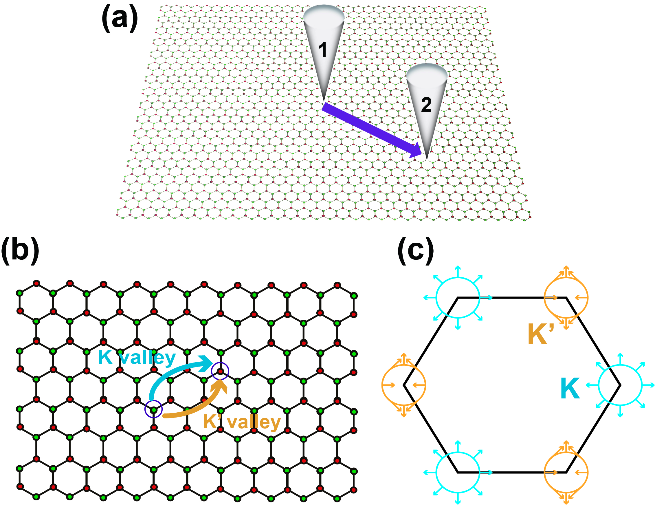
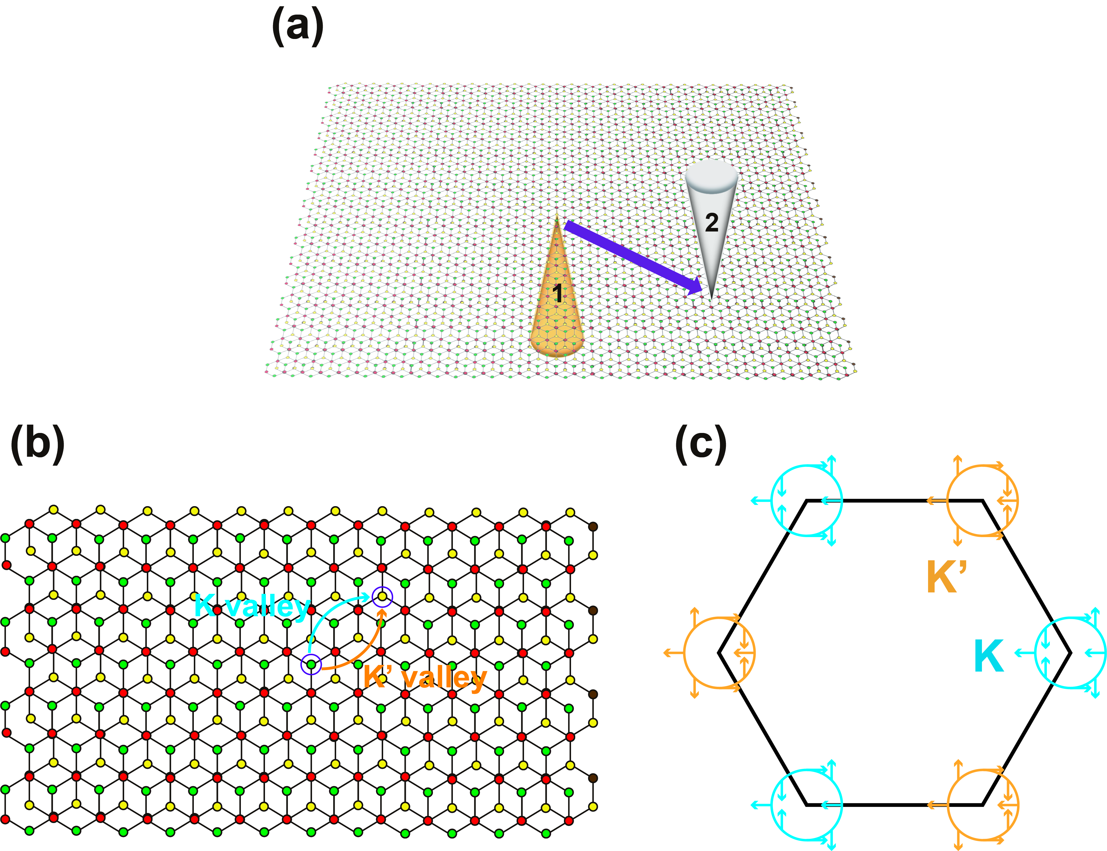
In this paper, we try to propose one scheme based on the transport measurement to detect wavefront dislocations in graphene systems. In previous experiments, transport methods usually manifest the topological properties of systems through a quantized two-terminal or Hall conductance [27, 28, 29, 30, 31, 32]. However, in our scheme, a conductance space map is necessary to be obtained. One promising solution is a dual-probe STM experiment with one fixed STM probe and one scanning STM probe [33, 34, 35, 36]. Since the graphene has a long mean free path [37, 38, 39], the interference effects are not washed out by dephasing when two STM tips are placed within a length scale [38, 24]. Both monolayer graphene and (biased) Bernal-stacked bilayer graphene are explored in our scheme. For the monolayer graphene, the fixed STM tip is connected to one sublattice and the scanning probe selectively scans the other sublattices around the fixed STM tip [Fig. 1(a)]. For the (biased) Bernal-stacked bilayer graphene, the fixed STM tip is connected to one sublattice of the bottom sheet and the scanning probe selectively scans the other sublattices on the top sheet around the fixed STM tip [Fig. 2(a)]. In both cases, due to the intervalley interference on the electron propagating path, wavefront dislocations emerge in the conductance map, reflecting the information of (local) topological indices. In fact, not limited to the dual-probe STM experiment, we emphasize that our scheme could be adapted to more similar systems.
Our paper is organized as follows. In Sec. II, we use the low-energy Hamiltonian of the monolayer graphene combined with nonequilibrium Green’s functions to analyze the transmission coefficients and the conductance between two sublattices. Using the tight-binding model, we numerically obtain the transmission coefficient/conductance maps and find they are well consistent with our analysis. In Sec. III, the same analysis and calculation procedure is reproduced on the Bernal-stacked bilayer graphene. We demonstrate that the wavefront dislocations are still robust even if the STM tip is coupled to multiple sublattices. This extends the practicality of our theoretical scheme. The case for biased bilayer graphene is also studied. In Sec. IV, we conclude a brief summary and give a discussion about the experiment realization.
II The monolayer graphene
In this section, we try to explore the wavefront dislocations in the dual-probe STM experiment of the monolayer graphene, as shown in Fig. 1(a). We first assume that each STM probe is only coupled to single sublattice, which is in principle possible in the experiments in view of STM atomic resolution. The case that the STM probes couple to multiple sublattices will be studied in next section. In fact, our theoretical proposal is not only limited on dual-probe STM experiment, but also applies to other similar systems, like the photonic graphene (see details about experiment implementations in Sec. IV).
A. Analytical analysis
The massless Dirac fermion in monolayer graphene can be demonstrated by the low-energy continuum Hamiltonian [40, 18]
| (1) |
which is written in the basis of sublattices . Here, the superscript M in the Hamiltonian as well as the following Green’s functions denotes the monolayer graphene. denote the valley indices and . is the Fermi velocity. is the momentum vector relative to the or . is the polar angle of electrons with the momentum . The eigenvalues of this low-energy Hamiltonian are with the corresponding eigenvectors . The eigenvectors define pseudospin vectors in the sublattice Bloch space , which has the pseudospin-momentum locking. Here is the vector of Pauli matrices acting on the sublattice space expanded by the basis . The pseudospin-momentum locking textures are shown in Brillouin zone for different valleys in Fig. 1(c). Along a closed Fermi surface, the pseudospin will rotate by yielding a winding number and Berry phase [40, 41, 42, 43].
To analyze the transport properties in the monolayer graphene, we calculate the bare retarded Green’s function matrix with [18]. It reads ( is the tip biased energy)
| (2) |
To do Fourier transformation, we use the integral [44, 20],
| (3) |
with the integer number , and . Note that this equation strictly holds for the case of the monolayer graphene (), but is an approximate formula for the case of the multilayer graphene () [44]. The Green’s functions of different valleys (i.e. in Eq. (2)) in the real space are [18],
| (4) |
where denotes the -th order Hankel function of the first kind. The polar angle related to the sublattice pseudospin mathematically transforms to the polar angle in the polar coordinate for the vector . It is worth noting that the real space singularity in off-diagonal matrix components is not physical, since the origin for the bare monolayer graphene is arbitrary. In Friedel oscillations, the origin is determined by a vacancy or an adatom. In transport measurement, e.g. dual-probe STM measurement, one of the probes (fixed STM probe) determines the location of the origin, while the other probe (scanning STM probe) scans around in real space.
Our main purpose is to extract the real space singularity resulting wavefront dislocations in the conductance map. In Fig. 1(a), if the fixed probe is connected to the sublattice and the scanning probe scans the sublattice , the transmission coefficient from probe to probe is [45, 35, 46, 47]
| (5) |
On the second line, the and are linewidth function matrices of the probes and coupled to graphene lattices. Here and respectively. is the linewidth function denoting the probe coupled to sublattices. is the retarded Green’s functions of the sample including the probe effects. and are the positions of scanning and fixed probes respectively. To simplify, assuming the effect of probes is weak, we neglect the influence of probes on sample Green’s functions, then
| (6) |
Here is the relative distance vector between two probes. Using the Fourier transform, we can obtain the Fourier components . Specially, at the is ( is a small number),
| (7) |
The last approximation is because the main Fourier components of Green’s functions focus on regions near the two valleys when the energy is relatively low. In the fast Fourier transform map of the STM experiment, should correspond to peaks around the intervalley interference points . Similar to previous references [18, 20], we do Fourier-filtering by only retaining the values of at the points around and discarding the other Fourier components. Then we do the inverse Fourier transform from them to obtain the Fourier transformed filtered transmission coefficient ,
| (8) |
where we use the relation . With the same operation, the Fourier transformed filtered transmission coefficient corresponding to can be obtained by just switching and ,
| (9) |
Substituting the bare Green’s functions in Eq. (4) into Eq. (8) and Eq. (9), the final intervalley filtered transmission coefficients we aim to obtain is
| (10) |
Analogically, if the fixed probe is connected to the sublattice and the scanning probe scans the sublattice , the intervalley filtered transmission coefficient is approximated as
| (11) |
In the experiment, we apply a small voltage on the scanning probe 1 and ground the fixed probe 2. Then we measure the current flowing into the fixed probe 2. The differential conductance could be calculated by Landauer-Bttiker formula at the zero temperature limit [45]. Thus in the following we only pay attention on the transmission coefficients map. Here the transmission coefficients or conductances exhibit a spatial oscillating behaviour via dependence. In Friedel oscillations, such a LDOS oscillation stems from the intervalley scatterings of electrons by vacancies or impurities [21, 18]. In the present transport device, the spatial oscillating behaviour comes from the intervalley interference on electron propagating paths [see Fig. 1(b)]. In addition, the propagation between A sublattice to B sublattice involves a relative phase in the momentum space and in the real space [see Eqs. (2) and (4)]. Such a relative phase originates from the fact that a gauge-invariant effective flux quantum always exist between A and B sublattice in the massless Dirac equation, whose sign is related to valley index [18]. It also reflects the distinct pseudospin-momentum locking texture for and valley as shown in Fig. 1(c). Thus, similar to the Friedel oscillations [18, 19], an additional phase enters the transmission coefficient in Eq. (10) as the twice of real space polar angle . The phase acts as a potential field whose gradient is the sum of a uniform field and a vortex [1], which is singular at . Considering the transmission coefficient is a single-valued function, it must return to the same value after circulating this field along a closed path. Thus, the path enclosing the field vortex should contribute to a phase quantized to a topological number with an integer . For , the phase accumulation in an anticlockwise direction is , corresponding to 4 times the Berry phase of the Dirac cone and 2 additional wavefronts. Conversely, no additional phase accumulation and wavefronts appear for , because no phase difference appears in the diagonal terms in Eq. (4).
B. The results of numerical simulations
To verify the above analytical analysis, we numerically calculate the transmission coefficient and its fast Fourier transform (FFT)-filtered images by using tight-binding model in this sub-section. We construct a finite graphene rectangular flake [as shown in Fig. 1(a, b)]. Here is the number of lattice along one side of rectangular graphene flake (the number of sites along the transverse and longitudinal direction is the same). In the calculations, we choose corresponding to the width and the length . The periodic boundary condition is applied (connecting the sites on the left and right boundaries, as well as the upper and lower boundaries respectively). Its nearest-neighbor hopping tight-binding Hamiltonian is
| (12) |
See Fig. 1(a), assuming that the fixed (scanning) probes () connect with two sublattice () respectively, their effects are quantized as the self-energy matrix , where or . The line-width matrix . We also introduce self-energy terms on the lattices at the flake edges, to simulate an open environment on graphene brought about by electrode contacts on the boundaries in the experiment. The retarded lattice Green’s function including all effects is
| (13) |
Then, the transmission coefficient from probe to probe is numerically calculated as [46, 47]. In the calculation detail, is the length of carbon-carbon bond. (Fermi velocity ), and . The tip biased energy . We here emphasize that our calculations are still in the low energy regime in view that and the Fermi momentum , which is much smaller than the intervalley distance . After obtaining the transmission coefficients at each site, we introduce a space broadening by , where denotes the space position of the scanning tip center relative to the origin determined by the fixed tip . Here .
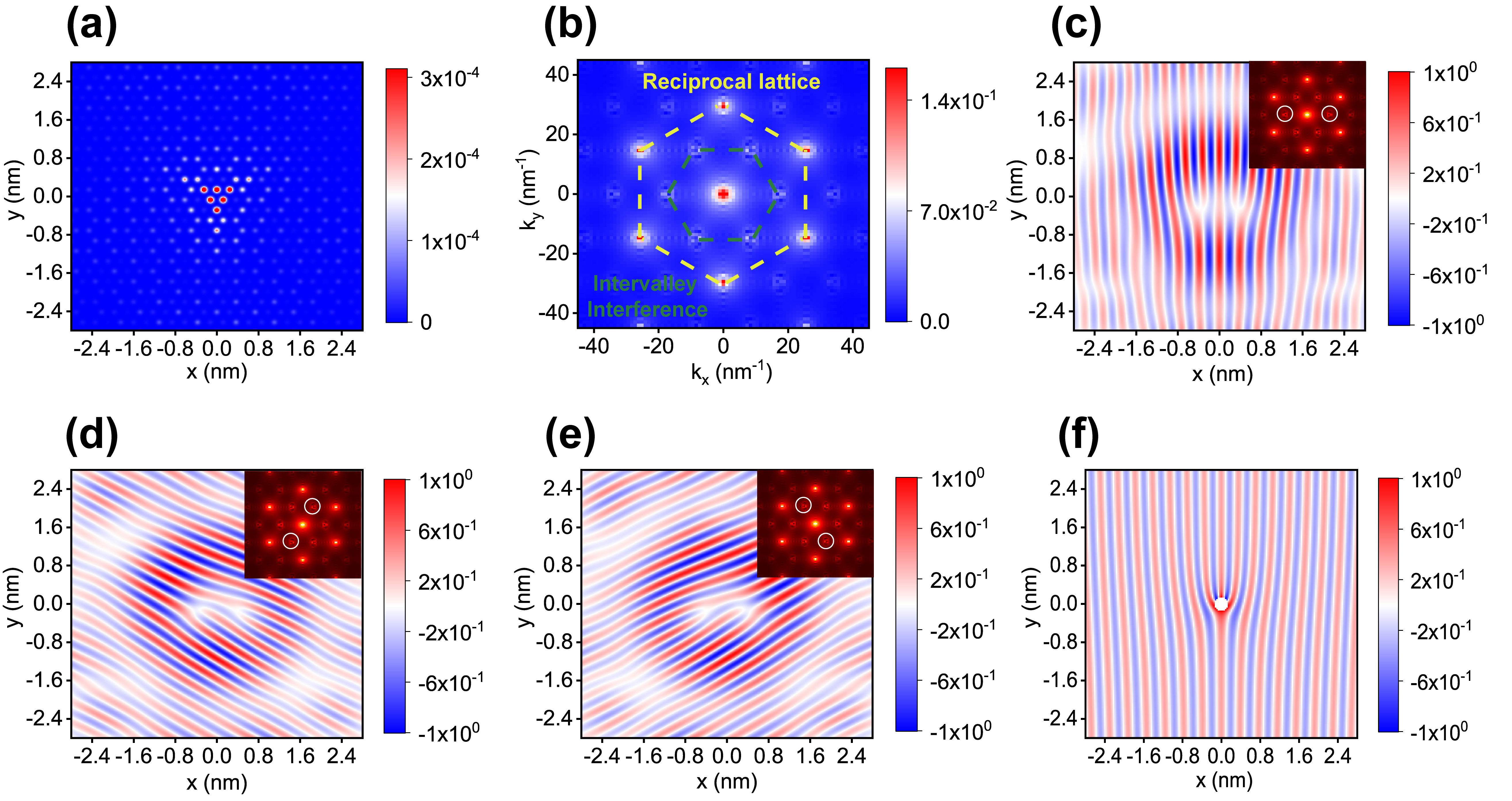
Now we briefly describe our FFT filtering method which follows the same procedure in Refs. [18, 20]. We first use the probe to scan a range of 6nm6nm to obtain the transmission coefficient (the conductance) in the real space [e.g. see Fig. 3(a)], and then use the FFT to obtain the image in the reciprocal space [e.g. see Fig. 3(b)]. Some bright spots denoting the main Fourier components could be found. We pay attention to six intervalley interference points [i.e. bright dots circled by green dashed lines in Fig. 3(b)]. Next, we take the filtering in the reciprocal space, that is, keep only the value in the white circles and set to zero outer the white circles [e.g. see the insets in Figs. 3(c-e)]. Note that two Fourier components with opposite momentum must be simultaneously included in the filtering process to ensure the FFT-filtered results are real, there will be three intervalley FFT-filtering directions [e.g. Figs. 3(c-e)]. Actually, these three directions reflect three intervalley interference processes since each point has three nearest-neighbour point in the Brillouin. In view that the phase singularity in Eq.(10) is irrelevant to , they are expected to exhibit similar characteristics of wavefront dislocations. In the calculations, the diameter of white circles is set to around . Finally, we take inverse FFT to obtain the oscillating transmission coefficient maps in the real space with the same size 6nm6nm [e.g. see Fig. 3(c-e)]. To avoid the inaccuracy on the boundaries, we focus on the range 5.6nm 5.6nm. In addition, all the analytical or numerical calculated FFT-filtered transmission coefficients plotted in the figures (including the next sections) are modulated as where is the maximum value of .
In Fig. 3(a), the fixed probe is connected to one sublattice and the scanning probe scans the surrounding sublattices. In the numerical calculated map, the is bright near the fixed probe at the origin and gradually weakens as the distance becomes farther away. This correlates with the decay relation implied by Hankel function of the first kind in Eq. (10). The modulus of the FFT of this transmission coefficient map is shown in Fig. 3(b). The bright spots in the FFT map indicates the main Fourier components [18, 48]. The yellow dashed lines connects the bright spots at the reciprocal lattices which reflect the information of graphene lattices. In addition, bright spots originated from the intervalley interference are connected by the green dashed lines. They are surrounded in a hexagon with a side length of that for reciprocal lattices. At the center, a bright ring denotes the intravalley scatterings, whose radius is roughly . Some discrepancies may be due to the scatterings and energy dissipations induced by the open environment at the graphene flakes boundaries. We focus on the intervalley interference and do the filtering around the white circles in the insets in Figs. 3(c-e) and then take the inverse FFT. The results show oscillating strip patterns with a wavelength of , which are just perpendicular to three FFT-filtered directions. Clearly, two additional wavefronts appear near the origin, where their positions are almost not affected by FFT-filtering directions as we expect. It indicates a phase accumulation related to a geometrical phase. The number of the additional wavefronts is well consistent with the analytical analysis in Eq. (10), plotted in Fig. 3(f) with .
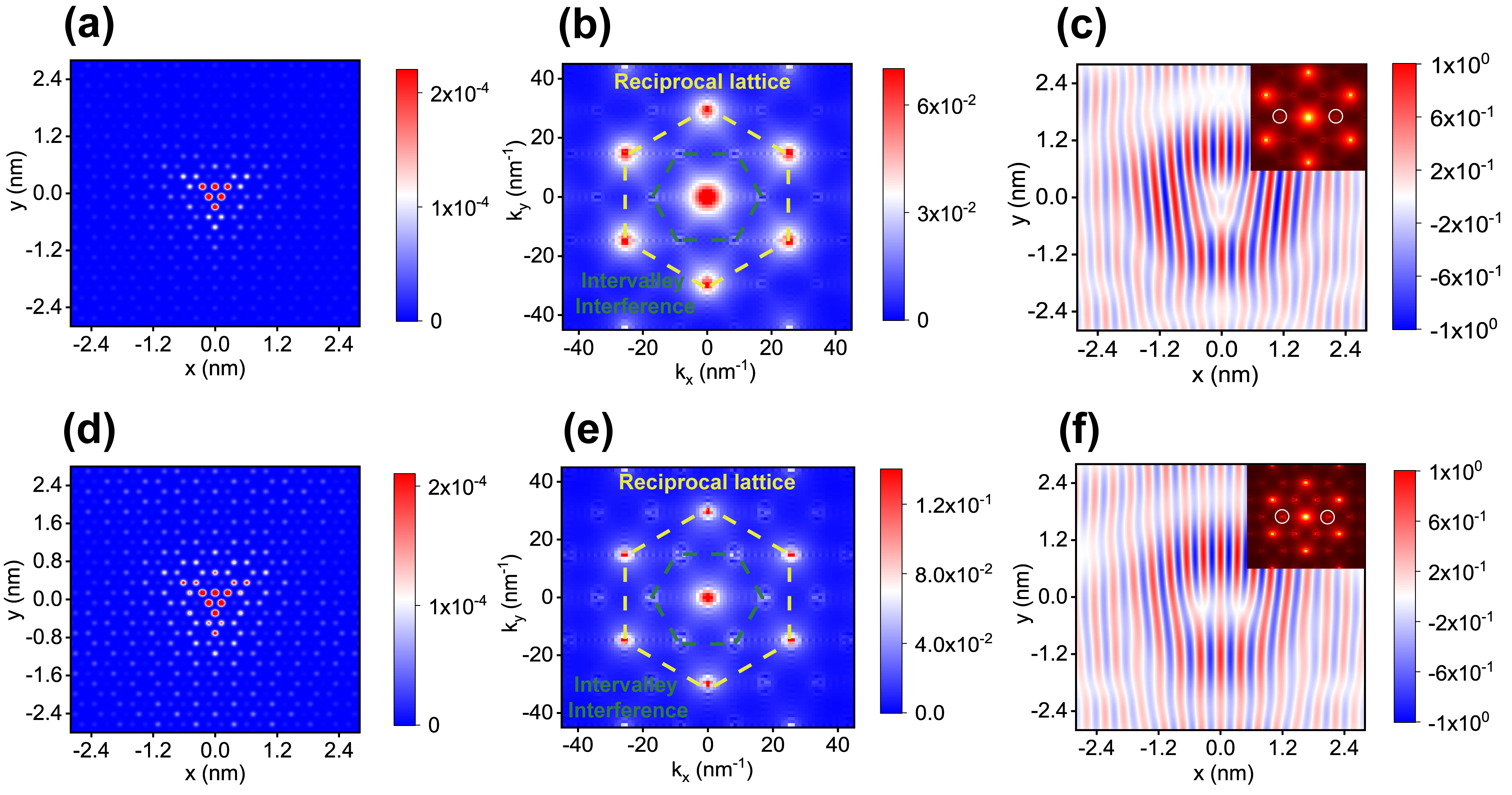
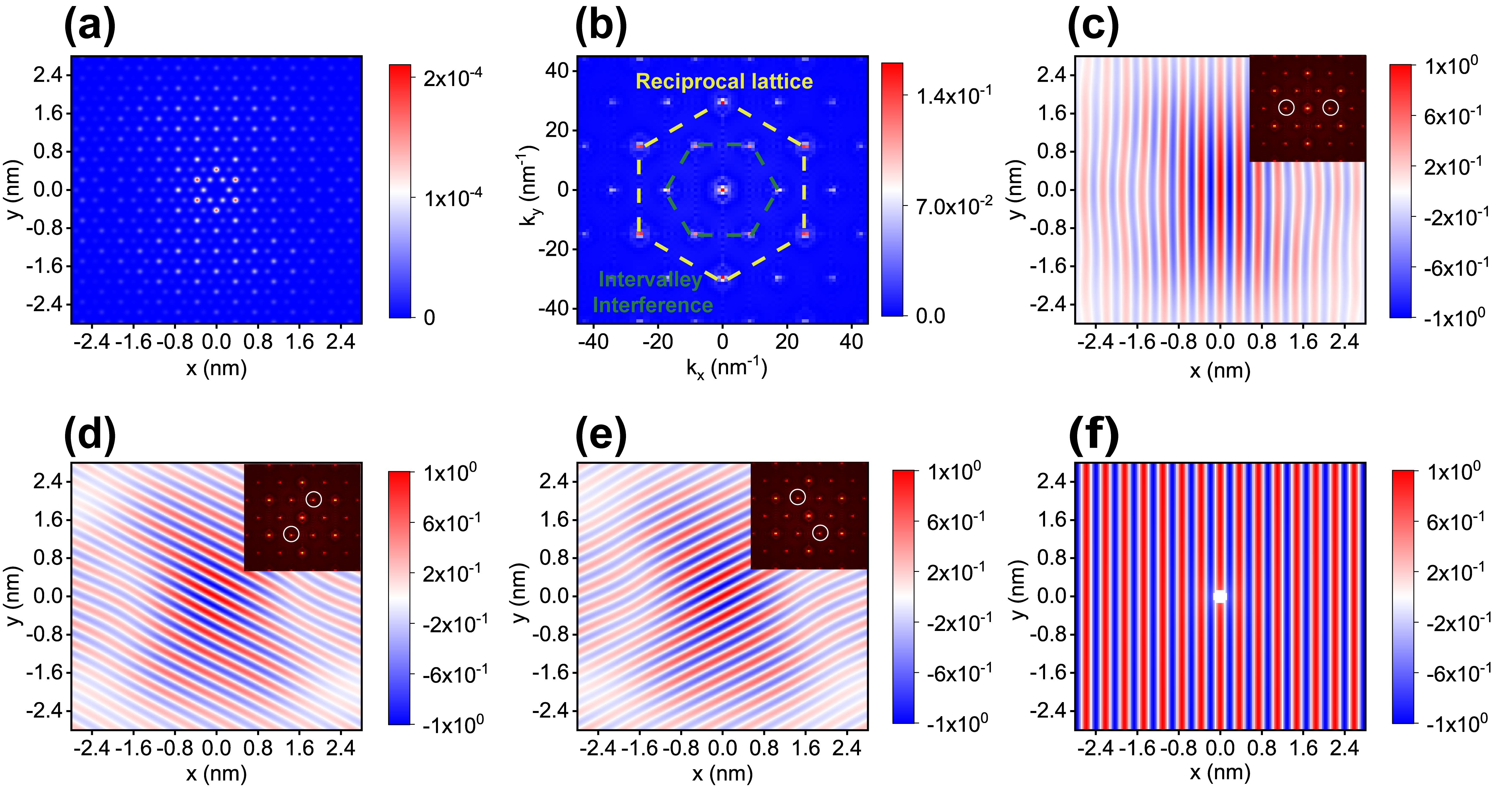
In Fig. 4(a), the fixed probe is selectively connected to one sublattice and the scanning probe scans the surrounding sublattices. Due to the change of scanned lattices, the transmission coefficient map shows peak positions slightly different from Fig. 3(a), but are still most bright near the center with . Because and lattices have the same periodic distributions, the FFT map of in Fig. 4(b) still contributes main Fourier components at reciprocal lattices (connected by yellow dashed lines) and intervalley interference points (connected by green dashed lines). However, after we do inverse FFT at the intervalley points circled by white circles in Figs. 4(c-e), although the periodic oscillating strips appear as well, no wavefront dislocations exhibit for all three filtering directions. It means that encircling the intervalley interference points no longer threads an additional geometric phase for transmission coefficients between the same kind sublattices. This is consistent with the analytical analysis in Eq. (11) plotted in Fig. 4(f).
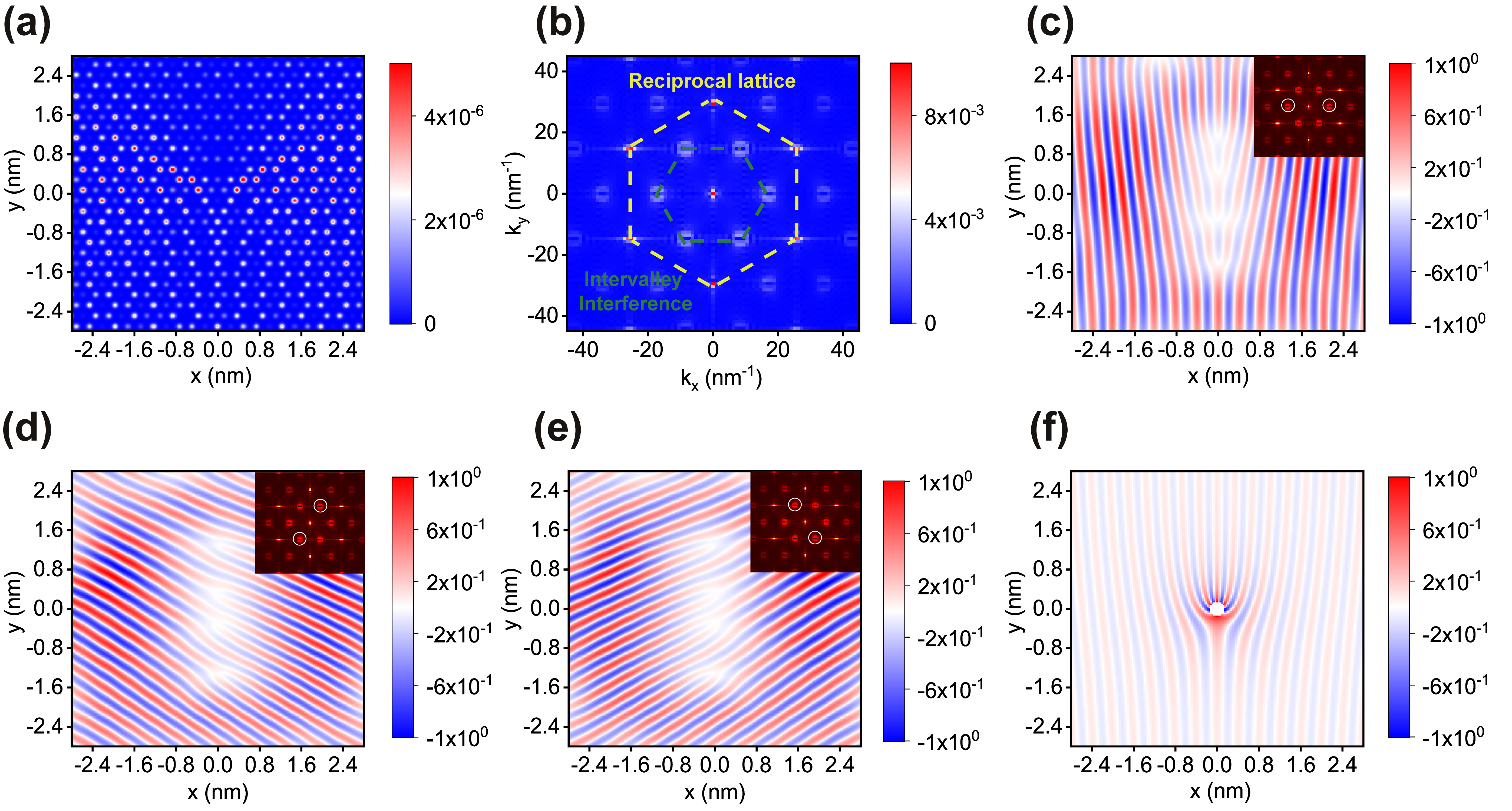
To investigate the effects of doping levels and sample sizes on our calculations, we present a numerical calculated transmission coefficient map of for a different tip biased energy and sample size in Fig. 5 to compared to Fig. 3. In Figs. 5(a-c), the tip biased energy and the sample size is the same as Fig. 3. In Figs. 5(d-f), we shorten the length of the graphene flake with sites along the longitudinal side and sites along the transverse side of the rectangle, then the size of the sample is . We can find the variation of the tip biased energy and sample size could affect the scatterings and energy dissipations on the boundary, thereby influencing the intensity of intervalley scatterings and intravalley scatterings [Figs. 5(b,e)]. However, the number of wavefront dislocations in FFT-filtered results is still 2 [see Figs. 5(c,f)], which is completely consistent with Fig. 3(c). This not only confirms the phase singularity is not affected by energy [Eq. (10)], but also confirms that our calculations have converged in size.
To conclude, the above results show that the phase singularities in the Green’s functions will not only enter LDOS in Friedel oscillations [18, 19], but also the transmission coefficients between different sublattices. The wavefront dislocations in the conductance map reflect the information of topological vortices. Enlightened by this, next we investigate the case for bilayer graphene.
III The Bernal-stacked Bilayer graphene
In this section, we generalize our theoretical setup to the Bernal-stacked bilayer graphene as shown in Fig. 2(a). Compared to monolayer graphene, two probes in the dual-probe STM experiment are connected to top and bottom layer of the bilayer graphene respectively. This separation makes the scanning of STM tips more convenient (see detailed discussions in Sec. IV). Moreover, we emphasize that the probe connected to the bottom graphene layer is not necessary to be a real STM tip. It could be replaced by a small electrode attached on the bottom sheet, serving as a drain in the transport measurement.
A. Analytical analysis of bilayer graphene
For the Bernal-stacked bilayer graphene, we consider that the sublattices of the top graphene sheet are located on top of the sublattices of the bottom graphene sheet. Then, the low-energy continuum Hamiltonian in the basis of is [49, 50]
| (14) |
where denotes the nearest-neighbour interlayer hopping. Here, the superscript D in the Hamiltonian as well as the following Green’s functions denotes the bilayer (double layer) graphene. At the condition , the Hamiltonian can be further projected on the basis [49]
| (15) |
with the eigenvalues and . Similar to monolayer graphene, the eigenvectors also define pseudospin vectors lying on the plane with an azimuth angle in the Bloch space. Here acts on the space expanded by the basis . This pseudospin-momentum locking texture is shown in Fig. 2(c). Particularly, after circulating a closed Fermi surface, the pseudospin rotates by , yielding a winding number and Berry phase [41]. The corresponding retarded Green’s functions of the bare bilayer graphene with the Hamiltonian in Eq. (14) can be calculated as
| (16) |
where . In the dual-probe STM measurements of bilayer graphene, we focus on four kinds of transmission coefficients , which means the fixed probe is connected to one sublattice or of the bottom layer and the scanning probe selectively scans sublattices or of the top layer. In analogy to Eqs. (8)-(10), their intervalley Fourier filtered terms are approximated as
| (17) |
By using Eq. (3) and taking the approximation for and [20], the corresponding Green’s functions of different valleys which are Fourier transformed from the momentum space in Eq. (LABEL:Eq16) to the real space are
| (18) |
Substituting the Eq. (18) into the Eq. (17), the analytic forms of intervalley Fourier filtered transmission coefficients are
| (19) |
As shown in Eq. (19), these transmission coefficients also exhibit periodically oscillating behavior due to the valley interference on electron propagating paths, see Fig. 2(b). But different from the case of monolayer graphene, the phase singularities in Eq. (19) suggest that additional wavefronts should appear near the origin in these kinds of transmission coefficients maps. The additional wavefronts are because the pseudospin vector of the bilayer graphene in Eq. (15) could accumulate times Berry phase along a path enclosing the origin. The and additional wavefronts can be understood as follows: the phase differences between () and () sublattices stay consistent with those in the monolayer graphene, since they are both distributed in the same top (bottom) sheet. The interlayer hopping links the phase between sublattices and sublattices. Based on this, the sublattices and , and ( and ), and could naturally possess a phase difference about , and , as shown in Eq. (LABEL:Eq16). Due to the intervalley interference on the electron propagating paths, it leads to the phase difference , and . additional wavefronts appear in the transmission coefficients , , , and , respectively. More generally, the above analysis can be extended to rhombohedral -layer graphene, which is expected to show , , , additional wavefronts due to Berry phase [20].
B. The results of numerical simulations
The numerical simulations follow a similar procedure as the case for monolayer graphene in Sec. II.B. Here we consider a finite bilayer graphene rectangular flake lattices (50 unit cells) along the longitudinal side and columns along the transverse direction of the flake. They correspond to the width and length respectively [Fig. 2(b)]. We also use the periodic boundary condition. By using the tight-binding model, we numerically calculate the transmission coefficient and its FFT-filtered images. In the numerical calculation, we set [20, 49], and . The tip biased energy corresponding to the Fermi momentum , which is much smaller than the intervalley distance. This ensures our calculations in the low energy regime. All the other parameters are the same as Fig. 3(b).
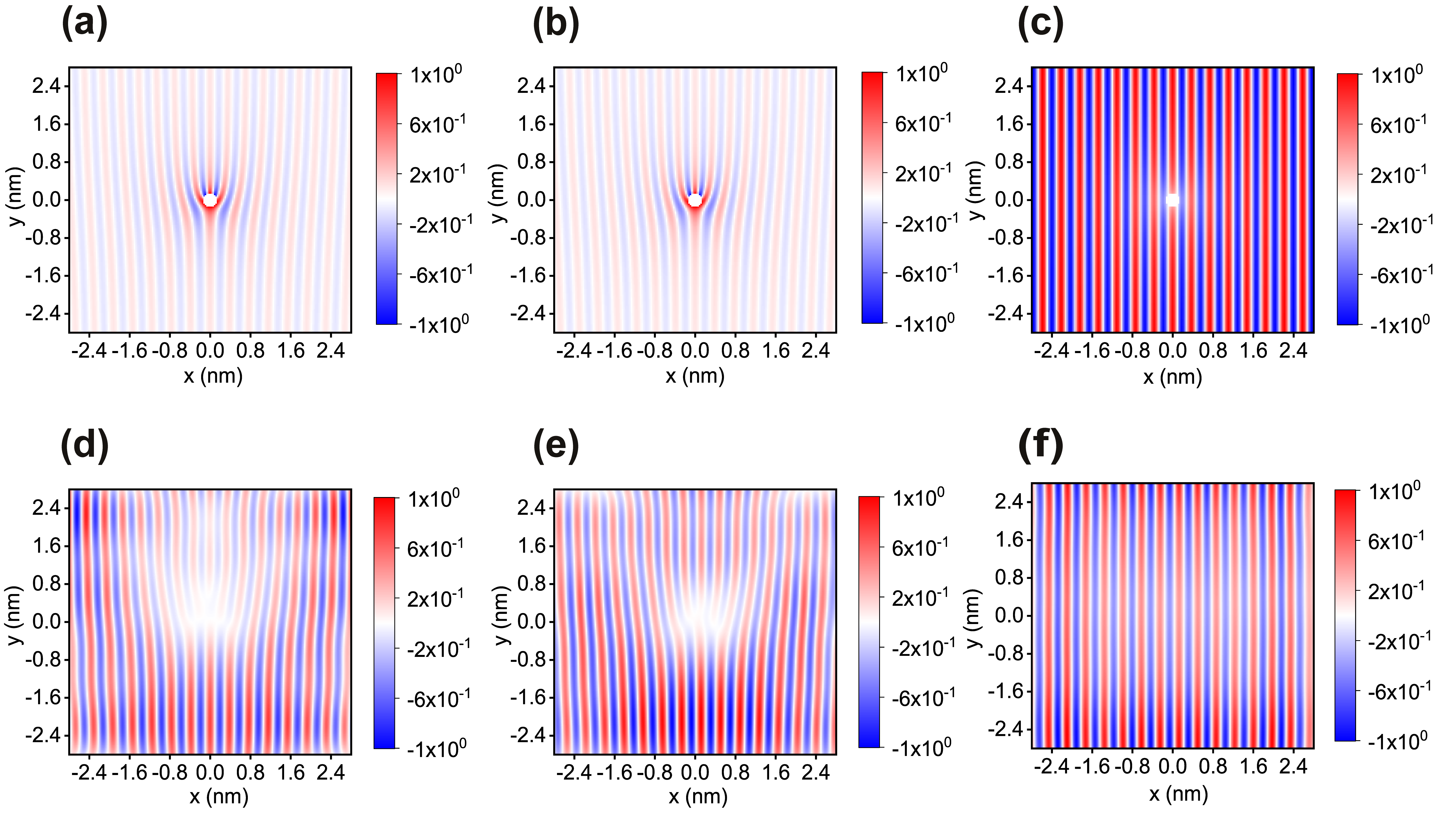
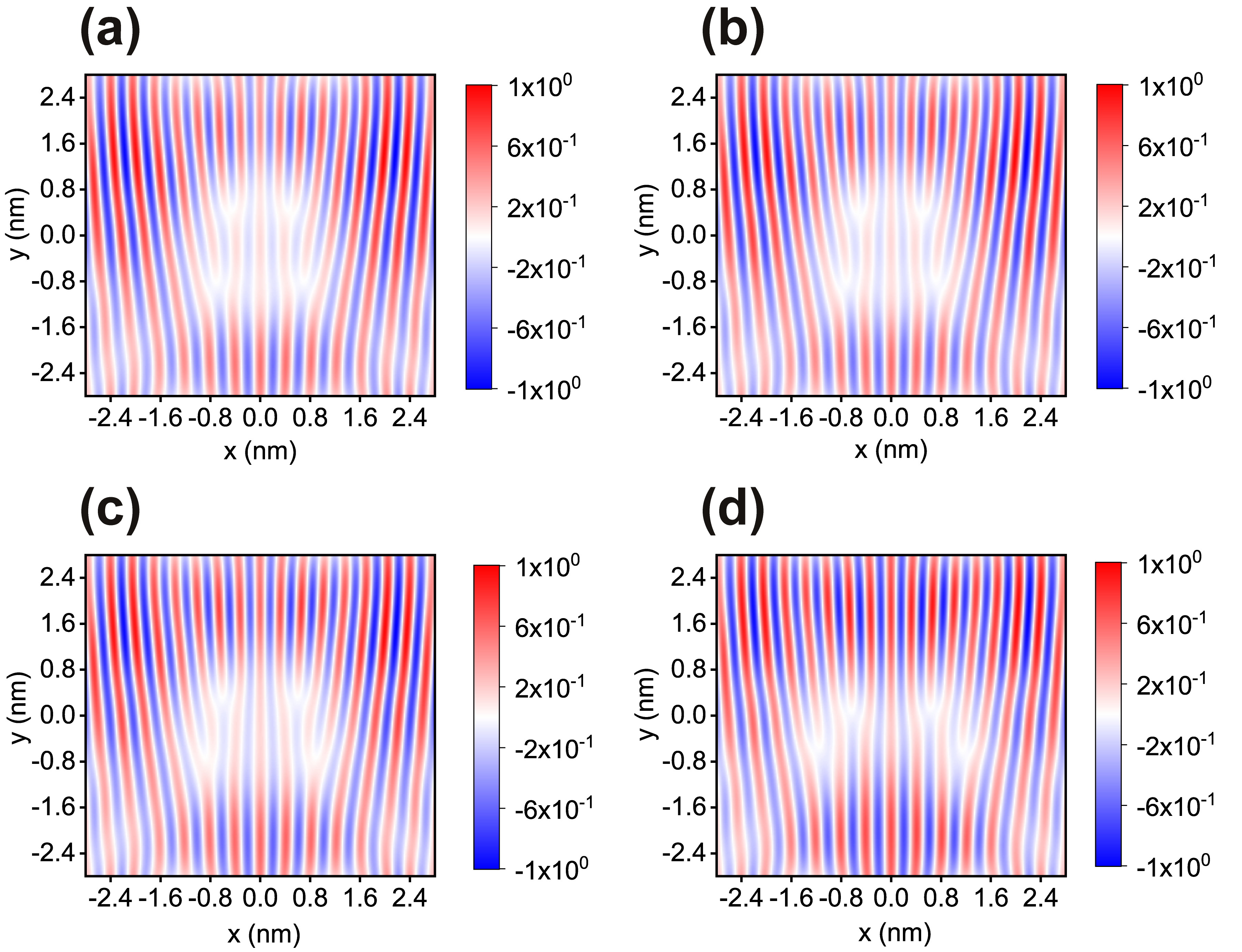
In Fig. 6(a), the transmission coefficient map of is shown, in which its strength still decays with the distance from the fixed probe. In the FFT map [Fig. 6(b)], we also find bright spots arranged as hexagons to denote main Fourier components for reciprocal lattices (connected by yellow dashed lines) and intervalley interference points (connected by green dashed lines) [20, 48]. Similar to the case of the monolayer graphene, a bright ring denoting intravalley scatterings also appear at the center. In Figs. 6(c-e), we show the intervalley filtered inverse FFT map at the white circles in each inset. Different from Fig. 3, four additional wavefronts emerge near the center for all three filtering directions, which indicates a 8 phase accumulation surrounding the origin. As proved in Sec. III.A, this geometric phase comes from intervalley interference between distinct pseudospin phase difference in bilayer graphene. Note that the positions of wavefronts do almost not change with the filtering direction. In theory, four additional wavefronts should all emerge exactly at the origin, as shown in Fig. 6(f) for the analytic form of in Eq. (19) with . The deviation for the locations of additional wavefronts in Figs. 6(c-e) may be attributed to the boundary effect.
Furthermore, the analytic forms of three transmission coefficients , and in Eq. (19) with are shown in Figs. 7(a-c). In comparison, the corresponding intervalley FFT-filtered numerical calculated transmission coefficients are shown in Figs. 7(d-f). Based on the symmetry, the results of and are basically same [see Eq. (19)]. Besides, two additional wavefronts arise, reflecting a phase accumulation surrounding the origin. This proves the phase differences between () and () indeed contribute a geometric phase 2. While for , no additional wavefronts exist, indicating the absence of the geometric phase. In total, all these characteristics confirm the validity of our analytical analysis.
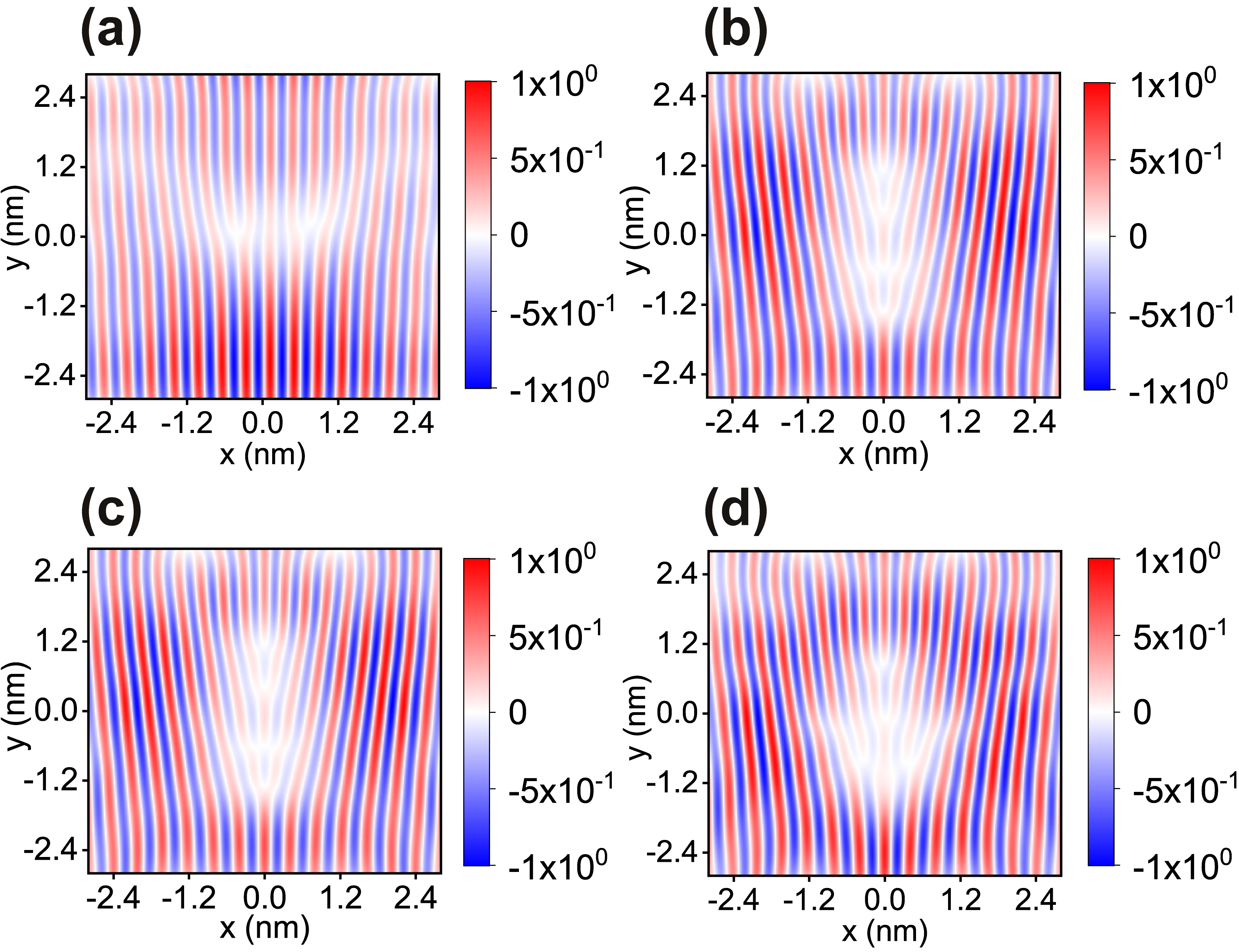
In a real scenario, because the STM tip has a finite size, it is difficult to couple to only one sublattice during the scanning process. But actually, even if the STM tip contact is not very ideal, our theoretical proposals in the bilayer graphene can still be applied. In Fig. 8, the fixed probe is connected with the sublattice in Fig. 8(a) and sublattice in Fig. 8(b), while the scanning probe scans all the sublattices surrounding the fixed probe. We denote these two transmission coefficients as and . In the maps, exhibits additional wavefront dislocations while exhibits additional wavefront dislocations. Moreover, besides the scanning tip, the fixed tip (or the electrode) may also couple to multiple sublattices. For example, in Fig. 8(c), the fixed probe or the electrode is coupled to one sublattice at the center and three surrounding sublattices in the meanwhile (the coupling strength to is set as half of the coupling strength to ). This transmission coefficient is denoted as and still exhibits additional wavefront dislocations. The above results are attributed to the fact that pseudospin components and of the wave function play a leading role as a relatively low energy, see Eqs. (14) and (15). This means in our settings when . So, although the probes may be coupled to multiple sublattices, and sublattices are more important than and sublattices.
Furthermore, we also investigate the case that the fixed probe or the electrode is coupled to the next-nearest-neighbour A’ sites. In Fig. 8(d), the fixed probe 1 is coupled to one central A’ site, its three nearest-neighbour B’ sites and six next-nearest-neighbour A’ sites on the bottom layer, while the scanning probe 2 scans all the lattices on the top layer (denoted as . The coupling strength of next-nearest-neighbour A’ sites is a half of that of nearest-neighbour B’ sites and a quarter of that of the central A’ site. We can find that such a coupling situation does not destroy 4 additional wavefronts near the center [see Fig. 8(d)]. Thus, even if coupled to multiple lattices, our scheme in bilayer graphene could still be robust. Of course, if the fixed probe or the electrode is very big to couple many carbon atoms, the expected results with 4 additional wavefronts may be buried. In terms of experimental realization, such a small electrode may be achieved by using a protrusion on the electrode to connect to a small area of the bottom sheet. It can be put right under the bilayer graphene, and covered by the insulating substrate. Under the substrate, the gating can adjust the doping level of the bilayer graphene [51, 52]. In total, we can expect that the dual-probe STM experiment is somewhat easier to achieve.
C. The biased bilayer graphene
In this subsection, to test the application range and robustness of our previous results, we further consider the biased bilayer graphene by applying a gate voltage in the out-of-plane direction. The electric field breaks the inversion symmetry and induces a continuously voltage-tunable band gap [53]. At the low energy range, the biased bilayer graphene with biased energy can be described by Hamiltonian [49]:
| (20) |
The bare retarded Green’s function matrix can be got as
| (21) |
where , and . It is easy to verify that once the biased energy , Eq. (20) and Eq. (LABEL:Eq21) directly restore to Eq. (14) and Eq. (LABEL:Eq16). Comparing Eq. (LABEL:Eq21) and Eq. (LABEL:Eq16), the biased voltage (i.e. the mass term) does not break the phase correlations of the Green’s function components, namely, and still have the phase , , and . This can be further illustrated by projecting the in Eq. (20) into the subspace expanded by the basis [49, 50],
| (22) |
Its eigenvalues are and eigenvectors are ), where . Although the pseudospin vectors defined by the eigenvectors are no longer pseudospin-momentum locking on the plane, they still have a azimuth angle. Since the winding number is invariant here, the same phase accumulation around the origin and the number of additional wavefronts will appear as the case for the biased energy .
In Fig. 9, we exhibit the numerical calculated FFT-filtered transmission coefficients map of . The energy and . At first, the biased voltage is absent with [Fig. 9(a)], the result should be similar to Fig. 6(c) where . We can find although the locations of wavefront dislocations change slightly, their number still keep four. This indicates our previous analysis does not depend on energy , which is similar to the monolayer graphene. Considering should exceed the energy gap to ensure the transport of the bulk states, we increase the from to in Figs. 9(b-d). Apparently, the number of additional wavefronts remains to be four during the variation. Therefore, the wavefront dislocations are robust in biased bilayer graphene for a range of the biased voltage. In fact, similar to the case of Friedel oscillations [54, 55], our scheme could be applied to other gapped two-dimensional materials, like gapped graphene and transition metal dichalcogenides.
IV Summary and Discussion
In this paper, we have raised a dual-probe scheme to demonstrate the wavefront dislocations in monolayer and Bernal-stacked bilayer graphene by the transport measurement. The analytical analysis shows that due to the distinct pseudospin textures at and valleys, the intervalley interference on the electron propagating paths could additionally introduce a phase singularity into transmission coefficients between different sublattices. This phase singularity acts as a topological defect and contributes additional wavefronts related to topological indices on the conductance map. A comprehensive numerical tight-binding calculations combined with FFT analysis further support our conclusions. Especially for the bilayer graphene, the wavefront dislocations is found to still exist even if the tips are connected to multiple sublattices. Our scheme is also applied for biased bilayer graphene and some other gapped two-dimensional materials. Our work opens up a new transport routine on experiment to explore valley-related topological properties of materials.
Now we will discuss the details about experimental implementation. In the current technical conditions, STM already allows imaging of the topography of surfaces, mapping the distribution of LDOS and manipulating individual atoms and molecules all at atomic resolutions [56, 57]. Therefore, the coupling of one atom site for the STM tip is in principle possible to be achieved in practice. The integration of several atomically precisely controlled probes in a multiprobe STM system has also continuously developed in recent years [33, 57]. To satisfy our scheme, the key point is the distance between the probes during the two-probe transport measurement. As reported by Kolmer at al, in two-probe STM/STS (Scanning tunneling spectroscopy) experiments on about 70nm long dangling bond dimer wire supported on a hydrogenated Ge(001) surface [58] and the anisotropic Ge(001) surface [59], the probe to probe separation distance could be reduced to tens of nanometers. The main limitation on the distance between STM probes is tip diameters. So, to achieve a smaller tip-tip distance, finer tips are required, which may cause some difficulties on implementation. However, such demanding condition are naturally relaxed in experiments on the bilayer graphene, since the two probes are spatially separated by the top and bottom graphene layers. Particularly, because the probes contact need not be limited on one site in bilayer graphene, the fixed probe connected to the bottom sheet as a source can also be replaced by a small electrode.
Photonic lattices [60, 61, 62] can also serve to implement our theoretical scheme. The photonic graphene is composed of a periodic array of evanescently-coupled waveguides in a honeycomb structure, which is often used to explore some fundamental wave-transport phenomena [63, 64]. Because the distance between each waveguide commonly reaches several , the light intensity at each lattice is easier to be obtained. In fact, there is a study to demonstrate the pseudo-mediated vortex generation in artificial photonic graphene by three or two beam excitation [65]. For our proposal, we can inject the light on one single waveguide of the input facet of the array, and measure the intensity profile at the output facet for desired sublattices. This process is equal to the finite-time evolution of an electron wavepacket and somehow similar to our proposed transport measurement.
Acknowledgments.
This work was financially supported by NSF-China (Grant No. 11921005), the Innovation Program for Quantum Science and Technology (2021ZD0302403), and the Strategic Priority Research Program of Chinese Academy of Sciences (Grant No. XDB28000000).
References
- Nye and Berry [1974] J. F. Nye and M. V. Berry, Dislocations in wave trains, Proc. R. Soc. Lond. A 336, 165 (1974).
- Berry et al. [1980] M. V. Berry, R. G. Chambers, M. D. Large, C. Upstill, and J. C. Walmsley, Wavefront dislocations in the Aharonov-Bohm effect and its water wave analogue, Eur. J. Phys. 1, 154 (1980).
- Berry [2017] M. V. Berry, Gauge-invariant Aharonov-Bohm streamlines, J. Phys. A Math. Theor. 50, 43LT01 (2017).
- Mawet et al. [2005] D. Mawet, P. Riaud, O. Absil, and J. Surdej, Annular groove phase mask coronagraph, Astrophysical J. 633, 1191 (2005).
- Berry [2000] M. Berry, Making waves in physics, Nature 403, 21 (2000).
- Melde et al. [2016] K. Melde, A. G. Mark, T. Qiu, and P. Fischer, Holograms for acoustics, Nature 537, 518 (2016).
- Jiménez-Gambín et al. [2020] S. Jiménez-Gambín, N. Jiménez, and F. Camarena, Transcranial focusing of ultrasonic vortices by acoustic holograms, Phys. Rev. Appl. 14, 054070 (2020).
- Padgett and Bowman [2011] M. Padgett and R. Bowman, Tweezers with a twist, Nat. Photonics 5, 343 (2011).
- Rafayelyan and Brasselet [2016] M. Rafayelyan and E. Brasselet, Bragg-Berry mirrors: reflective broadband q-plates, Opt. Lett. 41, 3972 (2016).
- Karjanto and van Groesen [2007] N. Karjanto and E. van Groesen, Note on wavefront dislocation in surface water waves, Phys. Lett. A 371, 173 (2007).
- Soskin et al. [2017] M. Soskin, S. V. Boriskina, Y. Chong, M. R. Dennis, and A. Desyatnikov, Singular optics and topological photonics, J. Opt. 19, 010401 (2017).
- Dennis et al. [2009] M. R. Dennis, K. O’Holleran, and M. J. Padgett, Singular optics: optical vortices and polarization singularities, Prog. Opt. 53, 293 (2009).
- Berry [1984] M. V. Berry, Quantal phase factors accompanying adiabatic changes, Proc. R. Soc. Lond. A 392, 45 (1984).
- Xiao et al. [2010] D. Xiao, M.-C. Chang, and Q. Niu, Berry phase effects on electronic properties, Rev. Mod. Phys. 82, 1959 (2010).
- Hasan and Kane [2010] M. Z. Hasan and C. L. Kane, Colloquium: Topological insulators, Rev. Mod. Phys. 82, 3045 (2010).
- Delplace et al. [2011] P. Delplace, D. Ullmo, and G. Montambaux, Zak phase and the existence of edge states in graphene, Phys. Rev. B 84, 195452 (2011).
- Li et al. [2014] L. Li, Z. Xu, and S. Chen, Topological phases of generalized Su-Schrieffer-Heeger models, Phys. Rev. B 89, 085111 (2014).
- Dutreix et al. [2019] C. Dutreix, H. González-Herrero, I. Brihuega, M. I. Katsnelson, C. Chapelier, and V. T. Renard, Measuring the Berry phase of graphene from wavefront dislocations in friedel oscillations, Nature 574, 219 (2019).
- Zhang et al. [2021a] Y. Zhang, Y. Su, and L. He, Quantum interferences of pseudospin-mediated atomic-scale vortices in monolayer graphene, Nano Lett. 21, 2526 (2021a).
- Zhang et al. [2020] Y. Zhang, Y. Su, and L. He, Local Berry phase signatures of bilayer graphene in intervalley quantum interference, Phys. Rev. Lett. 125, 116804 (2020).
- Friedel [1952] J. Friedel, Xiv. the distribution of electrons round impurities in monovalent metals, Philos. Mag. 43, 153 (1952).
- Dutreix and Delplace [2017] C. Dutreix and P. Delplace, Geometrical phase shift in Friedel oscillations, Phys. Rev. B 96, 195207 (2017).
- Dutreix et al. [2021] C. Dutreix, M. Bellec, P. Delplace, and F. Mortessagne, Wavefront dislocations reveal the topology of quasi-1D photonic insulators, Nat. Commun. 12, 3571 (2021).
- Clark et al. [2014] K. W. Clark, X.-G. Zhang, G. Gu, J. Park, G. He, R. M. Feenstra, and A.-P. Li, Energy Gap Induced by Friedel Oscillations Manifested as Transport Asymmetry at Monolayer-Bilayer Graphene Boundaries, Phys. Rev. X 4, 011021 (2014).
- Chen et al. [2017] L. Chen, P. Cheng, and K. Wu, Quasiparticle interference in unconventional 2D systems, J. Phys.: Condens. Matter. 29, 103001 (2017).
- Chen et al. [2021] W. Chen, X. Zhu, X. Zhou, and G. Zhou, Power law decay of local density of states oscillations near a line defect in a system with semi-Dirac points, Phys. Rev. B 103, 125429 (2021).
- Zhang et al. [2005] Y. Zhang, Y.-W. Tan, H. L. Stormer, and P. Kim, Experimental observation of the quantum Hall effect and Berry’s phase in graphene, Nature 438, 201 (2005).
- Fang et al. [2021] J.-Y. Fang, N.-X. Yang, Q. Yan, A.-M. Guo, and Q.-F. Sun, Thermal dissipation in the quantum Hall regime in graphene, Phys. Rev. B 104, 115411 (2021).
- König et al. [2007] M. König, S. Wiedmann, C. Brüne, A. Roth, H. Buhmann, L. W. Molenkamp, X.-L. Qi, and S.-C. Zhang, Quantum spin Hall insulator State in HgTe Quantum wells, Science 318, 766 (2007).
- Zhuang and Sun [2022] Y.-C. Zhuang and Q.-F. Sun, Phase diagrams and edge-state transitions in graphene with spin-orbit coupling and magnetic and pseudomagnetic fields, Phys. Rev. B 106, 165417 (2022).
- Law et al. [2009] K. T. Law, P. A. Lee, and T. K. Ng, Majorana Fermion Induced Resonant Andreev Reflection, Phys. Rev. Lett. 103, 237001 (2009).
- Mao and Sun [2021] Y. Mao and Q.-F. Sun, Charge and spin transport through a normal lead coupled to an -wave superconductor and a majorana zero mode, Phys. Rev. B 103, 115411 (2021).
- Nakayama et al. [2012] T. Nakayama, O. Kubo, Y. Shingaya, S. Higuchi, T. Hasegawa, C.-S. Jiang, T. Okuda, Y. Kuwahara, K. Takami, and M. Aono, Development and Application of Multiple-Probe Scanning Probe Microscopes, Adv. Mater. 24, 1675 (2012).
- Eder et al. [2013] F. R. Eder, J. Kotakoski, K. Holzweber, C. Mangler, V. Skakalova, and J. C. Meyer, Probing from Both Sides: Reshaping the Graphene Landscape via Face-to-Face Dual-Probe Microscopy, Nano Lett. 13, 1934 (2013).
- Settnes et al. [2014a] M. Settnes, S. R. Power, D. H. Petersen, and A.-P. Jauho, Theoretical analysis of a dual-probe scanning tunneling microscope setup on graphene, Phys. Rev. Lett. 112, 096801 (2014a).
- Settnes et al. [2014b] M. Settnes, S. R. Power, D. H. Petersen, and A.-P. Jauho, Dual-probe spectroscopic fingerprints of defects in graphene, Phys. Rev. B 90, 035440 (2014b).
- Mayorov et al. [2011] A. S. Mayorov, R. V. Gorbachev, S. V. Morozov, L. Britnell, R. Jalil, L. A. Ponomarenko, P. Blake, K. S. Novoselov, K. Watanabe, T. Taniguchi, and A. K. Geim, Micrometer-scale ballistic transport in encapsulated graphene at room temperature, Nano Lett. 11, 2396 (2011).
- Rickhaus et al. [2013] P. Rickhaus, R. Maurand, M.-H. Liu, M. Weiss, K. Richter, and C. Schönenberger, Ballistic interferences in suspended graphene, Nat. Commun. 4, 2342 (2013).
- Gunlycke et al. [2007] D. Gunlycke, H. M. Lawler, and C. T. White, Room-temperature ballistic transport in narrow graphene strips, Phys. Rev. B 75, 085418 (2007).
- Castro Neto et al. [2009] A. H. Castro Neto, F. Guinea, N. M. R. Peres, K. S. Novoselov, and A. K. Geim, The electronic properties of graphene, Rev. Mod. Phys. 81, 109 (2009).
- Park and Marzari [2011] C.-H. Park and N. Marzari, Berry phase and pseudospin winding number in bilayer graphene, Phys. Rev. B 84, 205440 (2011).
- Hou et al. [2019] Z. Hou, Y.-F. Zhou, X. C. Xie, and Q.-F. Sun, Berry phase induced valley level crossing in bilayer graphene quantum dots, Phys. Rev. B 99, 125422 (2019).
- Liu et al. [2020] Y.-W. Liu, Z. Hou, S.-Y. Li, Q.-F. Sun, and L. He, Movable Valley Switch Driven by Berry Phase in Bilayer-Graphene Resonators, Phys. Rev. Lett. 124, 166801 (2020).
- Dutreix and Katsnelson [2016] C. Dutreix and M. I. Katsnelson, Friedel oscillations at the surfaces of rhombohedral N-layer graphene, Phys. Rev. B 93, 035413 (2016).
- Datta [1995] S. Datta, Electronic Tansport in Mesoscopic Systems (Cambridge University Press, England, 1995).
- Long et al. [2008] W. Long, Q.-f. Sun, and J. Wang, Disorder-induced enhancement of transport through graphene junctions, Phys. Rev. Lett. 101, 166806 (2008).
- Sun and Xie [2010] Q.-f. Sun and X. C. Xie, -Invariant Quantum Spin Hall Effect in Ferromagnetic Graphene, Phys. Rev. Lett. 104, 066805 (2010).
- Mallet et al. [2012] P. Mallet, I. Brihuega, S. Bose, M. M. Ugeda, J. M. Gómez-Rodríguez, K. Kern, and J. Y. Veuillen, Role of pseudospin in quasiparticle interferences in epitaxial graphene probed by high-resolution scanning tunneling microscopy, Phys. Rev. B 86, 045444 (2012).
- Rozhkov et al. [2016] A. V. Rozhkov, A. O. Sboychakov, A. L. Rakhmanov, and F. Nori, Electronic properties of graphene-based bilayer systems, Phys. Rep. 648, 1 (2016).
- Nilsson et al. [2008] J. Nilsson, A. H. Castro Neto, F. Guinea, and N. M. R. Peres, Electronic properties of bilayer and multilayer graphene, Phys. Rev. B 78, 045405 (2008).
- Zhang et al. [2009] Y. Zhang, T.-T. Tang, C. Girit, Z. Hao, M. C. Martin, A. Zettl, M. F. Crommie, Y. R. Shen, and F. Wang, Direct observation of a widely tunable bandgap in bilayer graphene, Nature 459, 820 (2009).
- Wong et al. [2020] D. Wong, K. P. Nuckolls, M. Oh, B. Lian, Y. Xie, S. Jeon, K. Watanabe, T. Taniguchi, B. A. Bernevig, and A. Yazdani, Cascade of electronic transitions in magic-angle twisted bilayer graphene, Nature 582, 198 (2020).
- Castro et al. [2007] E. V. Castro, K. S. Novoselov, S. V. Morozov, N. M. R. Peres, J. M. B. Lopes dos Santos, J. Nilsson, F. Guinea, A. K. Geim, and A. H. Castro Neto, Biased Bilayer Graphene: Semiconductor with a Gap Tunable by the Electric Field Effect, Phys. Rev. Lett. 99, 216802 (2007).
- Zhang et al. [2021b] S.-H. Zhang, J. Yang, D.-F. Shao, Z. Wu, and W. Yang, Robust wavefront dislocations of Friedel oscillations in gapped graphene, Phys. Rev. B 103, L161407 (2021b).
- Yang et al. [2021] J. Yang, D.-F. Shao, S.-H. Zhang, and W. Yang, Friedel oscillations in graphene gapped by breaking and symmetries: Topological and geometrical signatures of electronic structure, Phys. Rev. B 104, 035402 (2021).
- Hansma et al. [1988] P. K. Hansma, V. B. Elings, O. Marti, and C. E. Bracker, Scanning tunneling microscopy and atomic force microscopy: Application to biology and technology, Science 242, 209 (1988).
- Ko et al. [2019] W. Ko, C. Ma, G. D. Nguyen, M. Kolmer, and A.-P. Li, Atomic-scale manipulation and in situ characterization with scanning tunneling microscopy, Adv. Funct. Mater. 29, 1903770 (2019).
- Kolmer et al. [2017] M. Kolmer, P. Olszowski, R. Zuzak, S. Godlewski, C. Joachim, and M. Szymonski, Two-probe STM experiments at the atomic level, J. Phys.: Condens. Matter. 29, 444004 (2017).
- Kolmer et al. [2019] M. Kolmer, P. Brandimarte, J. Lis, R. Zuzak, S. Godlewski, H. Kawai, A. Garcia-Lekue, N. Lorente, T. Frederiksen, C. Joachim, D. Sanchez-Portal, and M. Szymonski, Electronic transport in planar atomic-scale structures measured by two-probe scanning tunneling spectroscopy, Nat. Commun. 10, 1573 (2019).
- Rechtsman et al. [2013a] M. C. Rechtsman, J. M. Zeuner, Y. Plotnik, Y. Lumer, D. Podolsky, F. Dreisow, S. Nolte, M. Segev, and A. Szameit, Photonic Floquet topological insulators, Nature 496, 196 (2013a).
- Polini et al. [2013] M. Polini, F. Guinea, M. Lewenstein, H. C. Manoharan, and V. Pellegrini, Artificial honeycomb lattices for electrons, atoms and photons, Nat. Nanotechnol. 8, 625 (2013).
- Wu and Hu [2015] L.-H. Wu and X. Hu, Scheme for Achieving a Topological Photonic Crystal by Using Dielectric Material, Phys. Rev. Lett. 114, 223901 (2015).
- Schwartz et al. [2007] T. Schwartz, G. Bartal, S. Fishman, and M. Segev, Transport and Anderson localization in disordered two-dimensional photonic lattices, Nature 446, 52 (2007).
- Rechtsman et al. [2013b] M. C. Rechtsman, J. M. Zeuner, A. Tünnermann, S. Nolte, M. Segev, and A. Szameit, Strain-induced pseudomagnetic field and photonic landau levels in dielectric structures, Nat. Photonics 7, 153 (2013b).
- Song et al. [2015] D. Song, V. Paltoglou, S. Liu, Y. Zhu, D. Gallardo, L. Tang, J. Xu, M. Ablowitz, N. K. Efremidis, and Z. Chen, Unveiling pseudospin and angular momentum in photonic graphene, Nat. Commun. 6, 6272 (2015).