Four-Terminal Graphene-Superconductor Thermal Switch Controlled by The Superconducting Phase Difference
Abstract
We propose a superconducting phase-controlled thermal switch based on a four-terminal graphene-superconductor system. By coupling two superconducting leads on a zigzag graphene nanoribbon, both the normal transmission coefficient and crossed Andreev reflection coefficient, which dominate the thermal conductivity of electrons in the graphene nanoribbon, can be well controlled simultaneously by the phase difference of the superconducting leads. As a result, the thermal conductivity of electrons in the graphene nanoribbon can be tuned and a thermal switching effect appears. Using the non-equilibrium Green’s function method, we verify this thermal switching effect numerically. At ambient temperatures less than about one-tenth of the superconducting transition temperature, the thermal switching ratio can exceed 2000. The performance of the thermal switch can be regulated by the ambient temperature, and dopping or gating can slightly promote the thermal switching ratio. The use of narrower graphene nanoribbons and wider superconducting leads facilitates obtaining larger thermal switching ratios. This switching effect of electronic thermal conductance in graphene is expected to be experimentally realized and applied.
I Introduction
A heat current can carry information and energy like an electric current. Thermotronics [1], which corresponds to electronics, is also expected to realize effects such as thermal diodes [2, 3, 4], negative differential thermal resistance [5, 6], thermal transistors [7], thermal logic gates [8, 9] and thermal memory [10, 11] based on heat currents. However, compared to the control of electric currents, the ability to control the heat currents is much weaker. The electronics is well-developed, while the thermotronics has only started in the last two decades [12]. In contrast to electronics, in thermal devices one does not have to worry about the deadly problem of heat dissipation. In the design process of most thermal devices, it is crucial to control the on/off of the heat current, i.e., to make a thermal switch or thermal valve [13].
A thermal switch can be defined as a device that connects a high temperature terminal (heat source) and a low temperature terminal (heat drain). By controlling some variables of the device, one can achieve significant control over the thermal conductivity of the device [14]. Many previous efforts have been made in the design of thermal switches, which can control thermal conductivity through many different variables, such as temperature itself [15] and many kinds of phase transitions (solid-liquid, ferromagnetic-paramagnetic, semiconductor-metal, etc.) brought by temperature [16, 17, 18, 19, 20, 21, 22], external electric or magnetic fields [23, 24, 25, 26, 27, 28], and the strain, pressure or twist of the materials [29, 30, 31, 32], etc. The main carriers of heat current are also different, including phonons [33], electrons [12], photons [12, 34] and even magnons [35], which makes the operating temperature of thermal devices cover an enormous range from milliKelvin to thousands of Kelvin, suitable for different occasions.
Superconductors are good thermal insulators at low temperatures [36], which naturally allows their application in the design of thermal devices. The study of the superconducting-phase-controlled thermal transport, especially for electronic thermal transport, is known as phase-coherent caloritronics [38, 37, 4, 7, 9, 40, 39]. Very recently, by coupling a normal lead to a notch of a superconducting ring, Ligato et al. experimentally demonstrated that the thermal conductivity of electrons of the normal lead can be significantly controlled by the magnetic flux of the superconducting ring [40]. Compared to other methods for thermal switch design, since the electronic temperature evolves much faster than the phononic temperature in superconducting systems [36, 38], phase-coherent caloritronics is expected to develop thermal switches that are more suitable for advanced applications, such as computing.
Graphene has gained much attention due to its unique band structure [41] in the last two decades. Although the thermal transport of graphene is phonon-dominated over a large temperature range, with the decrease of temperature and device size, electronic thermal conductivity plays an increasingly important role [42]. Due to the weak electron-phonon coupling, at low temperature, the heat in electrons is well isolated from phonons [43, 44, 45]. So the temperature and thermal conductance of electrons in graphene can be measured and utilized almost unaffected by phonons. At the same time, graphene can be grown on an insulating substrate, ensuring that the heat of electrons is difficult to leak into the substrate. Therefore, it is possible to achieve excellent superconducting-phase-controlled electronic thermal transport in a graphene-superconductor system.
In this paper, using a combination of graphene and superconductors, we propose a thermal switch based on the idea of phase-coherent caloritronics. The electric transport properties of the graphene-superconductor hybrid system have been studied by a lot of literatures, and many interesting phenomena have been exhibited, such as the specular Andreev reflection [46, 47, 48, 49] and the crossed Andreev reflection [50]. Here we study the thermal transport properties of electrons in a four-terminal graphene-superconductor system and propose a thermal switch device. The thermal transport properties and influence factors of the system controlled by superconducting phase difference have been analyzed theoretically and calculated numerically. By means of the non-equilibrium Green’s function method, it has been proved that the superconducting phase difference can remarkably control the thermal conductance of electrons in the graphene nanoribbon, and the suitable working environments have been explored. From our calculations, this four-terminal structure can achieve a thermal switching ratio of over 2000 under a low temperature at different on-site energy. In addition, the production of graphene nanoribbons with widths below ten nanometers [51, 52], the high-quality contact between graphene nanoribbons and superconductors [53, 54], the control of the phase difference [55, 40], and the measurement of electronic temperature [36, 34, 40, 44] are all experimentally feasible, and thus our model is realizable. The theoretical studies and numerical calculations we have performed will advance the understanding of graphene-superconductor systems and the utilization of thermotronics.
The paper is organized as follows. In Sec. II, we present the model and theory studied in this paper, define the structure of the model and Hamiltonian, and derive the specific formulas of the thermal conductance by combining the non-equilibrium Green’s function method with the Landauer-Büttiker formula. In Sec. III, the numerical results of this paper are presented. Based on the numerical results, the control ability of the superconducting phase difference on the thermal conductance is discussed, and the effects of ambient temperature, on-site energy and the size of the system on the thermal switching ratio are studied. Sec. IV concludes this paper.
II Model and formulation
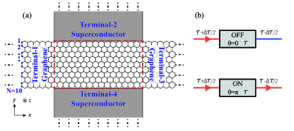
The thermal switching model we propose is a four-terminal graphene-superconductor system which consists of a zigzag graphene nanoribbon symmetrically coupled to two superconducting leads, as shown in Fig. 1(a). We set that there exists a superconducting phase difference between two superconducting leads. Experimentally, two superconducting leads can be connected to form a superconducting ring, so that the phase difference can be controlled by the magnetic flux through the ring [55, 40]. The phase difference can also be tuned by a supercurrent flowing through two superconducting leads. Fig. 1(b) shows the working principle of the thermal switch. A bias temperature is set so that graphene terminal-1 has a high temperature initially. When the superconducting phase difference , the thermal switch is switched off and the heat current can hardly flow from terminal-1 to terminal-3. When , the thermal switch is switched on and the thermal conductivity is significantly increased.
Using the nearest-neighbor tight binding method, the Hamiltonian of the system can be expressed as three parts [47]. , where , and are the Hamiltonians of the graphene nanoribbon [including the dashed red box and the graphene leads of terminal-1/3 in Fig. 1(a)], superconducting leads of terminal-, and the coupling between the superconducting lead terminal- and the graphene nanoribbon, respectively, with . They can be expressed as [47, 56]
| (1) | |||||
| (2) | |||||
| (3) |
where and are the on-site energy and the hopping energy in the graphene region. () and () are the creation (annihilation) operators in the graphene and the superconductor with the spin and the site index . Operators of superconducting leads can be transformed between momentum space and real space, , where is the coordinate at the site . We use -wave superconductors for superconducting leads, with the superconducting gap , and their phase difference .
According to the Landauer-Büttiker formula, the electric and heat current through terminal-1 can be obtained [47, 56, 57, 58]
| (4) | |||||
| (5) | |||||
where and represent the electron and the hole, respectively. is the chemical potential of terminal-1. We consider that a small bias voltage or a small bias temperature is applied on the graphene nanoribbon between the terminal-1 and terminal-3 and two superconductor terminals are set to be ground. The Fermi distributions of the superconductor terminals are , and the Fermi distributions in graphene terminals are and , with the temperature and voltage . When the bias voltage and the bias temperature are infinitesimal, the Fermi distribution can be approximated linearly [59]. Taking the electron as an example
| (6) |
where . When we consider the electric conductance, we take , , . When we consider the thermal conductance, we take , , and . We set all parts of the system except terminal-1/3 to maintain the ambient temperature . Then, we can express the conductance as
| (7) | |||||
| (8) | |||||
Different coefficients of transmissions and Andreev reflections in Eqs. (4, 5, 7, and 8) correspond to different physical processes, which can be calculated by the method of non-equilibrium Green’s function [47, 56, 57].
-
•
The normal transmission coefficient from terminal-1 to terminal-3, ;
-
•
The local Andreev reflection coefficient for the incident electron coming from terminal-1 with the hole Andreev reflected to terminal-1, ;
-
•
The crossed Andreev reflection coefficient for the incident electron coming from terminal-1 with the hole Andreev reflected to terminal-3, ;
-
•
The normal transmission coefficient from terminal-1 to a superconductor terminal, ;
where is the matrix of the linewidth function of the center region [the region surrounded by the dashed red box in Fig.1(a)] coupled to the terminal-, and is the matrix of the retarded (advanced) Green’s function of the center region. Here and have been expressed in Nambu representation, and subscriptions , , , respectively represent the four matrix elements of Nambu subspace with and for the electron and hole components.
In order to calculate the coefficients above, we need the matrix of surface Green’s function of each terminal, which can be obtained numerically [60]. Then, by combining the surface Green’s functions with the coupling Hamiltonian between the center region and the terminal-, the retarded self-energy can be calculated, whose matrix elements can be expressed as . And the linewidth function can be obtained together . Finally, with the Dyson equation, the retarded and advanced Green’s functions of the center region can be expressed as , where is the Hamiltonian of the center region.
With the formulas in this section, the electric and thermal conductance can be calculated. In the numerical calculations, we fix the superconducting gap , corresponding to a BCS transition temperature of about , which is common for conventional superconducting transition temperatures, such as plumbum [61]. The hopping energy of graphene is set to be as a typical value [41]. The hopping energy and lattice constants of the superconductors were selected to match the values of graphene, which lead to a similar BCS coherent length to previous studies [62] and much larger than the size of our system. The Dynes broadening parameter [63] (i.e. the imaginary part added to the energy when calculating the Green’s function) is set to , and it can be verified that the result calculated by this value is almost the same as those calculated with the common value [40, 39].
III Results and Discussions
In this section, the numerical calculations of the above model are performed, and the control of the superconducting phase difference on the thermal conductance of the system is given. In addition, the effect of ambient temperature , the on-site energy (dopping or gating) and the size of the center region on the performance of the thermal switch is investigated.
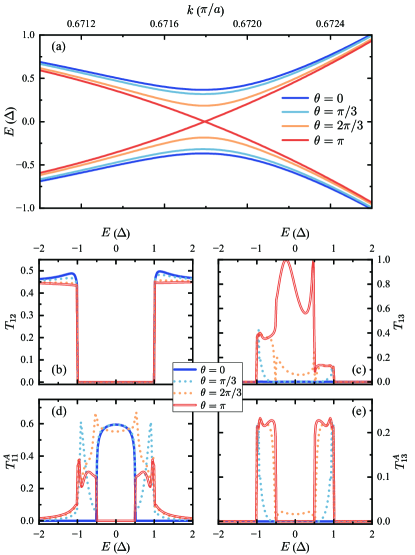
In Eqs. (7) and (8), we can see that the control of superconducting phase difference on the electric and thermal conductance is equivalent to the control of these transmission and Andreev reflection coefficients. Therefore, we need to investigate the effect of the superconducting phase difference on each coefficient, and the results are shown in Fig. 2. First, in Fig. 2(a), we present the band structure near the gap of the center graphene region [the dashed red box in Fig. 1(a)] proximitized by superconductors, which dominates the thermal switching effect. When calculating the energy band, we do not consider terminal-1 and terminal-3, and extend the center region and two superconductors coupled on the upper and lower sides (a SNS junction) infinitely in the horizontal () direction. Here, we use the upper and lower superconductors with discrete square lattices and the 28 lattices in the direction to provide the proximity effect. Thus, the horizontal wave vector becomes a good quantum number to obtain the solution of the energy band. The results show that, due to the superconducting proximity effect, the band opens a gap near the Fermi surface controlled by the superconducting phase difference . When , the gap is the largest, while the gap is closed when , which is consistent with the results of previous studies on SNS junctions [64]. Electrons and holes from terminal-1 need to tunnel through a barrier to transmit to terminal-3, when the gap is opened.
Fig. 2(b) shows the normal transmission coefficient from graphene terminal-1 to superconducting terminal-2 . Obviously, appears only outside the superconducting gap . The image of (not given) is similar to , and due to the geometric symmetry of our system, exactly. It can be seen that since the normal transmission into the superconductor involves only one superconducting terminal, the effect of the phase difference on is not significant. The normal transmission coefficient from graphene terminal-1 to graphene terminal-3 is shown in Fig. 2(c). As the superconducting phase difference increases in , the gap of the system gradually closes, and the barrier height that electrons need to tunnel through decreases [40, 64]. Therefore, increases dramatically with increasing . when , while is close to when , which achieves a good switching effect.
Figs. 2(d) and (e) show the coefficients of the local Andreev reflection and the crossed Andreev reflection , respectively. Since our system has the joint symmetry combined by the time-reversal operator with the mirror reflection about the plane or with the rotation of about the axis [65, 66], the Andreev reflection coefficients and are symmetrical about . With the increase of the phase difference in , is reduced to when the incident energy , and increases from 0 for , as a result of the constructive and destructive interference of reflected holes. This is because the superconductor-graphene interface can occur both intraband () Andreev retro-reflection (ARR) and interband () specular Andreev reflection (SAR) [46, 67]. When , ARR is eliminated by destructive interference and only SAR occurs. In contrast to ARR, the amplitude of SAR in a zigzag graphene nanoribbon with even chains has odd-parity under mirror operation [47, 68]. As a result, when , SAR is eliminated by destructive interference, and ARR reaches the maximum value. Due to the quantum diffraction effects, the reflected holes do not have definite directions, which makes holes of SAR (ARR) can also transmit to terminal-1(3), leading to the nonzero value of () in the region of SAR (ARR). However, considering the size of the center region, the barrier is long and multiple reflections can happen. Therefore, within is always much smaller than , and increases almost monotonically with the phase difference in [see Figs. 2(e)]. In addition, , have no tail outside , while has, which is because the first two are lost by multiple reflections, during the process of reaching terminal-3.
To sum up the results of Fig. 2, the superconducting phase difference significantly controls , , and , which mainly occur within the superconducting gap . Through the control of the gap at the center region and the interference of reflected holes, and increase almost monotonically as increases in . But the effect of phase difference on and is weak, which occurs only outside the superconducting gap. Next, combined with Eqs. (7) and (8), we can calculate and analyze the effect of phase difference on electric and thermal conductance.
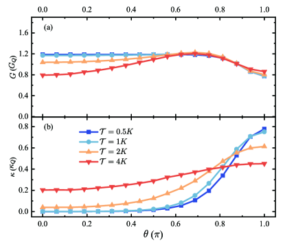
In Fig. 3, we show the variation of electric conductance and thermal conductance of electrons with the superconducting phase difference . It can be seen that the control of phase difference on each coefficient does not induce a good electric switch effect. This is because the superconducting phase difference has opposite control effects on and . As increases from 0 to , increase while decreases [shown in Fig. 2(c-e)]. As a result, we cannot observe the phase-controlled effect on the conductance because that is proportional to the sum of and as shown in Eq. (7). From the physical picture, this is because Cooper pairs are able to conduct electric currents in superconductors without being restricted by the energy gap of the center region. As opposed to the conductance , the superconducting phase difference achieves a significant on/off control of the thermal conductance at the appropriate temperature, similar to recent experiments [40]. This is because as increases from to , both the normal transmission coefficient and the crossed Andreev reflection coefficient are enhanced: Because of the energy gap closing, significantly increases from almost zero; Due to the constructive interference of reflected holes, also increases. From the physical picture, the Cooper pairs cannot conduct heat [36, 12], so that the thermal conductance is independent of the local Andreev reflection coefficient [see Eq. (8)] and can be well controlled by the energy gap of the center region. In addition, it can be seen in Fig. 3(b) that ambient temperature has a great influence on the performance of the thermal switch, which can be measured by the thermal switching ratio [14]. Next, we study the influence of ambient temperature and other variables on thermal switch performance by calculating .
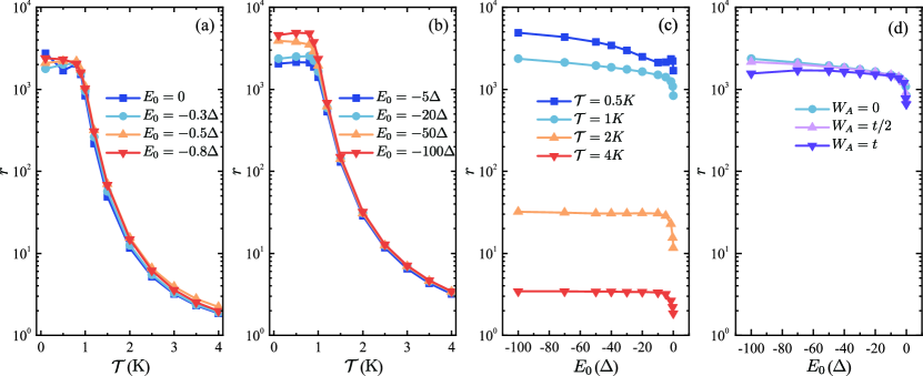
The calculation results of thermal switching ratio varying with ambient temperature is shown in Figs. 4(a) and 4(b). The thermal switch we devise mainly controls the heat current flowing in the graphene nanoribbon, which depends on the good thermal insulating performance of the superconductor at low temperatures [40]. As the temperature rises, the Fermi distribution widens. As a result, more electrons with energy outside are involved. We already know from the above discussion that the electrons outside are mainly transmitted normally into the superconductors and are hardly controlled by the phase difference, as shown in Fig. 2(b). Therefore, as shown in Figs. 4(a) and 4(b), with the increase of ambient temperature, the thermal switching ratio drops sharply with all on-site energies, which is consistent with the results of recent experiments [40]. When (about ), the thermal switch maintains good performance. For example, the thermal switching ratio can exceed 2000 at , which is much larger than that given by previous thermal switches (their ratio is usually less than 100) [16, 18, 22, 24]. Our considerations here are based on conventional superconductors (), but this device is also suitable for high- superconductors. With the large energy gap of high- superconductors, the sensitivity to temperature will be significantly reduced.
On the contrary, the increase of not only does not harm the thermal switching effect, but also slightly promotes its performance, and this part of the calculation results are shown in Fig. 4(c). For either the normal transmission or the crossed Andreev reflection, the incident electron or hole from the terminal-1 needs to pass through the barrier in the center region caused by the gap in order to reach terminal-3. Since the change in the on-site energy will not have a sufficient effect on the amplitude of the gap, our thermal switch can work at a large range of the on-site energies . In particular, the thermal switching ratio can always exceed 2000 regardless of at the low temperature [see the curve with in Fig.4(c)]. Increasing can increase the density of states of graphene, which is experimentally reflected in doping or adjusting the gate voltage, to increase the carrier concentration and then to enhance electronic thermal conductivity in the on and off states. However, the increase of the carrier concentration also enhances the superconducting proximity effect on graphene, so that the control of thermal conductivity by superconductors increases as well. As shown in Fig.4(c), with the increase of , the thermal switching ratio initially (when is small) has a rapid increase and soon tends to saturation.
In addition to the case of ballistic transport, we can further consider the presence of the impurities and diffusive transport caused by impurities and doping. We consider the case of Anderson disorder by adding a uniform random distributed term to the on-site energy in the center graphene region, i.e. , to simulate the effect of disorder on the system [48]. As shown in Fig.4(d), we fix the temperature , calculate and redraw the corresponding curve in Fig.4(c). With the increase of the disorder strength , the thermal switching ratio is slightly reduced, not surprisingly. However, the large thermal switching ratios survive even under a strong disorder for , which shows that the proposed thermal switch is not sensitive to disorder.
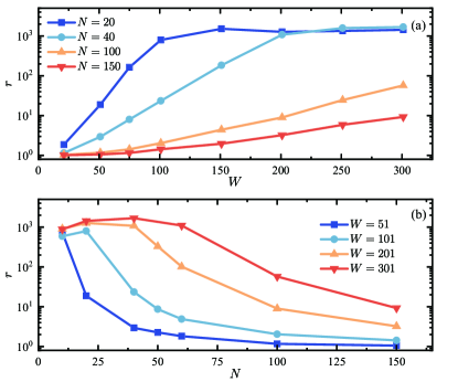
Last, let us study the influence of the size of the system on the performance of the thermal switch. In the discussion of Fig. 2, we mention that when the phase difference , the opened energy gap becomes a barrier through which electrons and holes need to pass in the center region. The size of the system has noticeable effects on the barrier. The height of the barrier, i.e., the amplitude of the gap opening in the center region, decreases exponentially with increasing the width of the graphene nanoribbon . And the barrier width is approximately equal to the width of the superconducting leads . Therefore, decreasing and increasing will inhibit heat current from passing through the center region when the energy gap is open at , which will allow the thermal switch to close better. On the contrary, when , the gap closes and the barrier vanishes. In the absence of an energy gap at the center region, changing and will have almost no effect on the opening of the thermal switch. Therefore, the thermal switching ratio will decrease with increasing and increase with increasing . Fig. 5 shows the results of the calculation for varying the system size. The variation of the thermal switching ratio is highly consistent with our analysis. In general, the choice of narrower graphene nanoribbons and wider superconducting leads allows the thermal switch to work better.
IV Conclusions
In summary, we propose a superconducting phase-controlled thermal switch which consists of a graphene nanoribbon coupled by two superconducting leads. When the superconducting phase difference decreases from to , the normal transmission coefficient (crossed Andreev reflection coefficient) decreases significantly to 0 due to the opening of the energy gap (destructive interference), then the thermal conductance of electrons in graphene nanoribbon also decreases significantly. Using the non-equilibrium Green’s function method, we have verified this thermal switching effect numerically. The results show that, the thermal switching ratio can exceed 2000, at ambient temperatures less than about one-tenth of the superconducting transition temperature. The performance of the thermal switch can be regulated by the ambient temperature, while the increase of the carrier concentration can slightly promote the thermal switching ratio. A narrower graphene nanoribbon and wider superconducting leads are favorable for obtaining a larger thermal switching ratio. In addition, the production of graphene nanoribbons with width below ten nanometers, the high-quality contact between graphene nanoribbons and superconductors, the control of the superconducting phase difference and the measurement of electronic temperature are all experimentally feasible, which provides conditions for realizing our model and high thermal switching ratio. Our work deepens the understanding of graphene-superconductor systems and provides theoretical support for the research of thermotronics.
ACKNOWLEDGMENTS
This work was financially supported by National Natural Science Foundation of China (Grant No. 12374034 and No. 11921005), the Innovation Program for Quantum Science and Technology (2021ZD0302403), and the Strategic Priority Research Program of Chinese Academy of Sciences (Grant No. XDB28000000).
References
- [1] J. Ordonez-Miranda, Y. Ezzahri, J. A. Tiburcio-Moreno, K. Joulain, and J. Drevillon, Radiative thermal memristor, Phys. Rev. Lett. 123, 025901 (2019).
- [2] B. Li, L. Wang, and G. Casati, Thermal diode: Rectification of heat flux, Phys. Rev. Lett. 93, 184301 (2004).
- [3] C. W. Chang, D. Okawa, A. Majumdar, and A. Zettl, Solid-state thermal rectifier, Science 314, 1121 (2006).
- [4] A. Fornieri, M. J. Martínez-Pérez, and F. Giazotto, Electronic heat current rectification in hybrid superconducting devices, AIP Adv. 5, 053301 (2015).
- [5] B. Li, L. Wang, and G. Casati, Negative differential thermal resistance and thermal transistor, Appl. Phys. Lett. 88, 143501 (2006).
- [6] H.-H. Fu, D.-D. Wu, Z.-Q. Zhang, and L. Gu, Spin-dependent Seebeck effect, thermal colossal magnetoresistance and negative differential thermoelectric resistance in zigzag silicene nanoribbon heterojunciton, Sci. Rep. 5, 10547 (2015).
- [7] F. Paolucci, G. Marchegiani, E. Strambini, and F. Giazotto, Phase-tunable temperature amplifier, Europhys. Lett. 118, 68004 (2017).
- [8] L. Wang and B. Li, Thermal logic gates: Computation with phonons, Phys. Rev. Lett. 99, 177208 (2007).
- [9] F. Paolucci, G. Marchegiani, E. Strambini, and F. Giazotto, Phase-tunable thermal logic: Computation with heat, Phys. Rev. Appl. 10, 024003 (2018).
- [10] L. Wang and B. Li, Thermal memory: A storage of phononic information, Phys. Rev. Lett. 101, 267203 (2008).
- [11] V. Kubytskyi, S.-A. Biehs, and P. Ben-Abdallah, Radiative bistability and thermal memory, Phys. Rev. Lett. 113, 074301 (2014).
- [12] J. P. Pekola and B. Karimi, Colloquium: Quantum heat transport in condensed matter systems, Rev. Mod. Phys. 93, 041001 (2021).
- [13] T. Swoboda, K. Klinar, A. S. Yalamarthy, A. Kitanovski, and M. M. Rojo, Solid-state thermal control devices, Adv. Electron. Materials 7, 2000625 (2020).
- [14] G. Wehmeyer, T. Yabuki, C. Monachon, J. Wu, and C. Dames, Thermal diodes, regulators, and switches: Physical mechanisms and potential applications, Appl. Phys. Rev. 4, 041304 (2017).
- [15] W.-R. Zhong, D.-Q. Zheng, and B. Hu, Thermal control in graphenenanoribbons: Thermal valve, thermal switch and thermal amplifier, Nanoscale 16, 5217-5220 (2012).
- [16] R. Zheng, J. Gao, J. Wang, and G. Chen, Reversible temperature regulation of electrical and thermal conductivity using liquid–solid phase transitions, Nat. Commun. 2, 289 (2011).
- [17] B. T. Ng, Z. Y. Lim, Y. M. Hung, and M. K. Tan, Phase change modulated thermal switch and enhanced performance enabled by graphene coating, RSC Adv. 6, 87159 (2016).
- [18] K. Kim and M. Kaviany, Thermal conductivity switch: Optimal semiconductor/metal melting transition, Phys. Rev. B 94, 155203 (2016).
- [19] S. Lee, K. Hippalgaonkar, F. Yang, J. Hong, C. Ko, J. Suh, K. Liu, K. Wang, J. J. Urban, X. Zhang, C. Dames, S. A. Hartnoll, O. Delaire, and J. Wu, Anomalously low electronic thermal conductivity in metallic vanadium dioxide, Science 355, 371 (2017).
- [20] Z. Hu, M. Hiramatsu, X. He, T. Katase, T. Tadano, Keisuke Ide, H. Hiramatsu, H. Hosono, and T. Kamiya, Reversible thermal conductivity modulation of non-equilibrium (Sn1-xPbx)S by 2D–3D structural phase transition above room temperature, ACS Appl. Energy Mater. 6, 3504 (2023).
- [21] X. Zhao, J. C. Wu, Z. Y. Zhao, Z. Z. He, J. D. Song, J. Y. Zhao, X. G. Liu, X. F. Sun, and X. G. Li, Heat switch effect in an antiferromagnetic insulator Co3V2O8, Appl. Phys. Lett. 108, 242405 (2016).
- [22] L. Castelli, Q. Zhu, T. J. Shimokusu, and G. Wehmeyer, A three-terminal magnetic thermal transistor, Nat. Commun. 14, 393 (2023).
- [23] J. F. Ihlefeld, B. M. Foley, D. A. Scrymgeour, J. R. Michael, B. Mckenzie, D. L. Medlin, M. Wallace, S. Trolier-Mckinstry, and P. E. Hopkins, Room-temperature voltage tunable phonon thermal conductivity via reconfigurable interfaces in ferroelectric thin films, Nano Lett. 15, 1791 (2015).
- [24] C. Liu, Y. Chen, and C. Dames, Electric-field-controlled thermal switch in ferroelectric materials using first-principles calculations and domain-wall engineering, Phys. Rev. Applied 11, 044002 (2019).
- [25] B. M. Foley, M. Wallace, J. T. Gaskins, E. A. Paisley, R. L. Johnson-Wilke, J. W. Kim, P. J. Ryan, S. Trolier-Mckinstry, P. E. Hopkins, and J. F. Ihlefeld, Voltage-controlled bistable thermal conductivity in suspended ferroelectric thin-film membranes, ACS Appl. Mater. Interfaces, 10, 25493 (2018).
- [26] A. N. McCaughan, V. B. Verma, S. M. Buckley, J. P. Allmaras, A. G. Kozorezov, A. N. Tait, S. W. Nam, and J. M. Shainline, A superconducting thermal switch with ultrahigh impedance for interfacing superconductors to semiconductors, Nat. Electron. 2, 451 (2019).
- [27] H. T. Huang, M. F. Lai, Y. F. Hou, and Z. H. Wei, Influence of magnetic domain walls and magnetic field on the thermal conductivity of magnetic nanowires, Nano Lett. 15, 2773 (2015).
- [28] R. Bosisio, S. Valentini, F. Mazza, G. Benenti, R. Fazio, V. Giovannetti, and F. Taddei, Magnetic thermal switch for heat management at the nanoscale, Phys. Rev. B 91, 205420 (2015).
- [29] X. Liu, G. Zhang, and Y. W. Zhang, Graphene-based thermal modulators, Nano Res. 8, 2755 (2015).
- [30] Y. Zeng, C.-L. Lo, S. Zhang, and Z. Chen, Dynamically tunable thermal transport in polycrystalline graphene by strain engineering, Carbon, 158, 63 (2020).
- [31] A. Ott, Y. Hu, X.-H. Wu, and S.-A. Biehs, Radiative thermal switch exploiting hyperbolic surface phonon polaritons, Phys. Rev. Applied 15, 064073 (2021).
- [32] Y. Du, J. Peng, Z. Shi, and J. Ren, Twist-induced near-field radiative heat switch in hyperbolic antiferromagnets, Phys. Rev. Applied 19, 024044 (2023).
- [33] N. Li, J. Ren, L. Wang, G. Zhang, P. Hänggi, and B. Li, Colloquium: Phononics: Manipulating heat flow with electronic analogs and beyond, Rev. Mod. Phys. 84, 1045 (2012).
- [34] A. Ronzani, B. Karimi, J. Senior, Y.-C. Chang, J. T. Peltonen, C. Chen, and J. P. Pekola, Tunable photonic heat transport in a quantum heat valve, Nat. Phys. 14, 991 (2018).
- [35] R. Jin, Y. Onose, Y. Tokura, D. Mandrus, P. Dai, and B. C. Sales, In-plane thermal conductivity of Nd2CuO4: Evidence for magnon heat transport, Phys. Rev. Lett. 91, 146601 (2003).
- [36] F. Giazotto, T. T. Heikkilä, A. Luukanen, A. M. Savin, and J. P. Pekola, Opportunities for mesoscopics in thermometry and refrigeration: Physics and applications, Rev. Mod. Phys. 78, 217 (2006).
- [37] A. Fornieri and F. Giazotto, Towards phase-coherent caloritronics in superconducting circuits, Nat. Nanotechnol. 12, 944 (2017).
- [38] C. Guarcello, P. Solinas, A. Braggio, M. Di Ventra, and F. Giazotto, Josephson thermal memory, Phys. Rev. Applied 9, 014021 (2018).
- [39] E. Strambini, F. S. Bergeret, and F. Giazotto, Proximity nanovalve with large phase-tunable thermal conductance, Appl. Phys. Lett. 105, 082601 (2014).
- [40] N. Ligato, F. Paolucci, E. Strambini, and F. Giazotto, Thermal superconducting quantum interference proximity transistor, Nat. Phys. 18, 627 (2022).
- [41] A. H. Castro Neto, F. Guinea, N. M. R. Peres, K. S. Novoselov, and A. K. Geim, The electronic properties of graphene, Rev. Mod. Phys. 81, 109 (2009).
- [42] T. Y. Kim, C.-H. Park, and N. Marzari, The electronic thermal conductivity of graphene, Nano Lett. 16, 2439 (2016).
- [43] J. K. Viljas and T. T. Heikkilä, Electron-phonon heat transfer in monolayer and bilayer graphene, Phys. Rev. B 81, 245404 (2010).
- [44] K. C. Fong and K. C. Schwab, Ultrasensitive and wide-bandwidth thermal measurements of graphene at low temperatures, Phys. Rev. X 2, 031006 (2012).
- [45] S. Yiğen, V. Tayari, J. O. Island, J. M. Porter, and A. R. Champagne, Electronic thermal conductivity measurements in intrinsic graphene, Phys. Rev. B 87, 241411(R) (2013).
- [46] C. W. J. Beenakker, Specular Andreev reflection in graphene, Phys. Rev. Lett. 97, 067007 (2006).
- [47] S.-G. Cheng, Y. Xing, J. Wang, and Q.-F. Sun, Controllable Andreev retroreflection and specular Andreev reflection in a four-terminal graphene-superconductor hybrid system, Phys. Rev. Lett. 103, 167003 (2009).
- [48] S.-G. Cheng, H. Zhang, and Q.-F. Sun, Effect of electron-hole inhomogeneity on specular Andreev reflection and Andreev retroreflection in a graphene-superconductor hybrid system, Phys. Rev. B 83, 235403 (2011).
- [49] Q. Cheng and Q.-F. Sun, Specular Andreev reflection and its detection, Phys. Rev. B 103, 144518 (2021).
- [50] W.-T. Lu and Q.-F. Sun, Electrical control of crossed Andreev reflection and spin-valley switch in antiferromagnet/superconductor junctions, Phys. Rev. B 104, 045418 (2021).
- [51] X. Li, X. Wang, L. Zhang, S. Lee, and H. Dai, Chemically derived, ultrasmooth graphene nanoribbon semiconductors, Science 319, 1229 (2008).
- [52] J. W. Bai, X. F. Duan, and Y. Huang, Rational fabrication of graphene nanoribbons using a nanowire etch mask, Nano Lett. 9, 2083 (2009).
- [53] F. Miao, S. Wijeratne, Y. Zhang, U. C. Coskun, W. Bao, and C. N. Lau, Phase-coherent transport in graphene quantum billiards, Science 317 1530 (2007).
- [54] F. Amet, C. T. Ke, I. V. Borzenets, J. Wanf, K. Watanabe, T. Taniguchi, R. S. Deacon, M. Yamamoto, Y. Bomze, S. Tarucha, and G. Finkelstein, Supercurrent in the quantum Hall regime, Science 352 966 (2016).
- [55] F. Giazotto, J. T. Peltonen, M. Meschke, and J. P. Pekola, Superconducting quantum interference proximity transistor, Nat. Phys. 6 254 (2010).
- [56] Q.-F. Sun and X. C. Xie, Quantum transport through a graphene nanoribbon–superconductor junction, J. Phys.: Condens. Matter 21, 344204 (2009).
- [57] Y. Meir and N. S. Wingreen, Landauer formula for the current through an interacting electron region, Phys. Rev. Lett. 68, 2512 (1992). A.-P. Jauho, N. S. Wingreen, and Y. Meir, Time-dependent transport in interacting and noninteracting resonant-tunneling systems, Phys. Rev. B 50, 5528 (1994).
- [58] N.-X. Yang, Q. Yan, and Q.-F. Sun, Half-integer quantized thermal conductance plateau in chiral topological superconductor systems, Phys. Rev. B 105, 125414 (2022).
- [59] M.-M. Wei, Y.-T. Zhang, A.-M. Guo, J.-J. Liu, Y. Xing, and Q.-F. Sun, Magnetothermoelectric transport properties of multiterminal graphene nanoribbons, Phys. Rev. B 93, 245432 (2016).
- [60] D. H. Lee and J. D. Joannopoulos, Simple scheme for surface-band calculations. II. The Green’s function, Phys. Rev. B 23, 4997 (1981).
- [61] N. W. Ashcroft and N. D. Mermin, Solid state physics, (Saunders College, 1976).
- [62] G.-H. Lee and H.-J. Lee, Proximity coupling in superconductor-graphene heterostructures, Rep. Prog. Phys. 81 056502 (2018).
- [63] R. C. Dynes, J. P. Garno, G. B. Hertel, and T. P. Orlando, Tunneling study of superconductivity near the metal-insulator transition, Phys. Rev. Lett. 53, 2437 (1984).
- [64] H. le Sueur, P. Joyez, H. Pothier, C. Urbina, and D. Esteve, Phase controlled superconducting proximity effect probed by tunneling spectroscopy, Phys. Rev. Lett. 100, 197002 (2008).
- [65] Q. Cheng, Q. Yan, and Q.-F. Sun, Spin-triplet superconductor–quantum anomalous Hall insulator–spin-triplet superconductor Josephson junctions: transition, phase, and switching effects, Phys. Rev. B 104, 134514 (2021).
- [66] W.-T. Lu and Q.-F. Sun, Spin polarization and Fano–Rashba resonance in nonmagnetic graphene, New J. Phys. 25, 043018 (2023).
- [67] C. W. J. Beenakker, Colloquium: Andreev reflection and Klein tunneling in graphene, Rev. Mod. Phys. 80, 1337 (2008).
- [68] Y. Xing, J. Wang, and Q.-F. Sun, Parity of specular Andreev reflection under a mirror operation in a zigzag graphene ribbon, Phys. Rev. B 83, 205418 (2011).