Standalone mobile quantum memory system
Abstract
We present the implementation and performance analysis of a portable, rack-mounted standalone warm vapor quantum memory system, that also includes the laser package, control electronics and data processing hardware. The optical memory is based on long-lived hyperfine ground states of Cesium which are connected to an excited state via the line at in a -configuration. The memory is operated with weak coherent pulses containing on average photons per pulse. The long-term stability of the memory efficiency and storage fidelity is demonstrated at the single-photon level together with operation in a non-laboratory environment.
I Introduction
Quantum memories (QMs) Lvovsky et al. (2009); Lei et al. (2023) are central to many applications in quantum information science from quantum sensing Mazelanik et al. (2021); Barzel et al. (2024), computation Nunn et al. (2013); Gouzien and Sangouard (2021) to long-distance quantum networking Sangouard et al. (2011); Muralidharan et al. (2016); Borregaard et al. (2020). To date, many realizations of QMs have been demonstrated with different physical systems, ranging from cold atomic ensembles Yang et al. (2016); Distante et al. (2017); Vernaz-Gris et al. (2018); Wang et al. (2019); Zhang et al. (2024) to solid-state systems Gündoğan et al. (2015); Jobez et al. (2015); Stas et al. (2022); Ortu et al. (2022); Zhou et al. (2023). As a necessary element of quantum repeaters, these devices should be able to operate in non-laboratory environments, and as such their future deployment in space could advance global quantum communication networks Gündoğan et al. (2021); Liorni et al. (2021); Gündoğan et al. (2021); Wallnöfer et al. (2022); Gündoǧan et al. (2024). In this context, warm-vapor QMs Reim et al. (2011); Wolters et al. (2017); Kaczmarek et al. (2018); Finkelstein et al. (2018); Guo et al. (2019); Wang et al. (2022); Buser et al. (2022); Thomas et al. (2023); Esguerra et al. (2023) are particularly promising due to their low complexity and low size, weight and power (SWaP). Unlike many other systems, they do not require laser or cryogenic cooling, which makes them attractive for practical applications. The key performance metrics for quantum memories include efficiency, fidelity, storage time, and multimode capacity. While there have been significant advancements in enhancing each of these metrics, here we shift the focus to another crucial aspect: the long-term stability and reliable operation of a fully integrated system outside a controlled laboratory setting. Although a rack-mounted memory system has been recently demonstrated Wang et al. (2022), to the best of our knowledge, operation of such a device with all of its subsystems fully integrated into a single, portable platform outside the laboratory environment has not been reported in the literature before.
II System Design
The rack-mounted memory system, shown in figure 1, features a laser system, a memory module, a spectral filtering module, and control electronics. The laser and the filtering systems are implemented with an emphasis on achieving high mechanical stability and robustness against environmental changes using similar technologies as reported in Pahl et al. (2019). The control electronics include a fast arbitrary waveform generator, laser current driver and locking electronics, temperature controller, and a time tagger. The system is designed to function as a testbed for future implementation of miniaturized components with a reduced SWaP budget; therefore, a fast oscilloscope is included in the rack and can be used to optimize the memory operation with bright pulses for the single-photon level storage experiments. A custom-made, python-based software controls all aspects of the experiment. The individual optical subsystems are presented in the following sections.
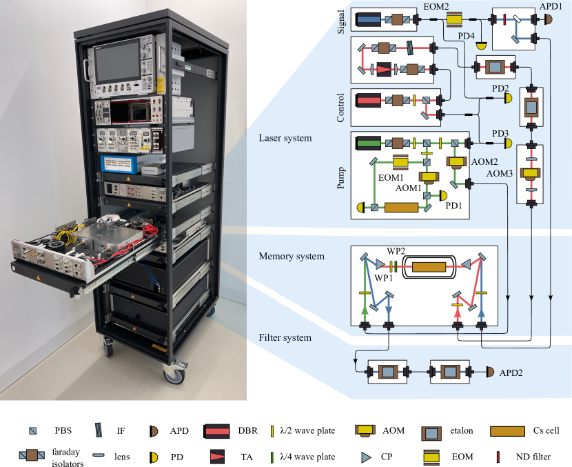
II.1 Laser system
The compact laser system is housed in the central section of the rack depicted in figure 1 and includes three distributed Bragg reflector (DBR) laser diodes to provide the required optical fields at different frequencies for the pump, control and signal pulses. The pump laser serves as an absolute frequency reference, stabilized to the hyperfine transition of the 133Cs line using frequency modulation spectroscopy detected on photodiode 1 (cf. figure 2 (b)). The light is modulated using a free-space electro-optic modulator (EOM1) with a modulation frequency of . An acousto-optic modulator (AOM2) driven at is used to switch the pump laser, providing of optical power to the memory module. To ensure that the pump light is on resonance after the AOM2, a AOM (AOM1) is included in the locking scheme as depicted in figure 1.
The control laser is offset-locked to the pump laser via the photo diode PD3 and amplified using a tapered amplifier (TA). In order to remove the amplified spontaneous emission from the TA an interference filter (IF) with a full-width at half-maximum (FWHM) bandwidth of and two monolithic Fabry-Pérot etalon with a finesse of and free spectral ranges (FSR) of and are used. Gaussian control pulses with a minimum FWHM of are temporally shaped using a free-space AOM (AOM3). The maximum continuous wave optical power distributed to the memory module is and decreases with shorter pulses due to the reduction of the AOM efficiency.
The signal laser is offset-locked to the control laser via PD2 and pulses are shaped using a fiber-coupled amplitude EOM (EOM2). The bias voltage of the EOM is locked to the minimum of the EOM transfer curve using a lock-in amplifier Snoddy et al. (2007) via PD4. Automated locking of all three lasers as well as the EOM bias is realized via a FPGA-based tool Wiegand et al. (2022). A combination of neutral density (ND) filters are used to attenuate the bright input pulses to create weak coherent states (WCS) with controllable mean input photon numbers, , for storage experiments. A monitor path with a splitting ratio (memory path/monitor path) of enables the calibration of on an avalanche photo diode (APD1) with a detection efficiency of .
II.2 Memory system
At the core of the memory system is a -long cylindrical glass cell with an inner diameter of and anti reflection coated windows containing 133Cs atoms and buffer gas. The cell is embedded in a copper rod and enclosed in three layers of mu-metal to prevent any spin wave decoherence through stray magnetic fields. Resistive heaters are mounted at the extremities of the rod that reach outside of the magnetic shield to allow heating of the cell without creating disruptive magnetic fields.
The perpendicular, linearly polarized, co-propagating signal and control beams are superposed via a calcite prism (CP) and focused at the center of the memory cell with a FWHM diameters of and respectively. Possible changes in the polarization due to the interaction with the atoms or the cell windows are counteracted using a combination of a quarter- and a half-wave plate (WP1 and WP2 in figure 1). A collimated counter-propagating linearly polarized pump beam with a FWHM diameter of and a power of overlaps with the signal and control beams.
II.3 Filter system and detection
To separate the strong control field from the signal field we use a combination of consecutive polarization and spectral filtering to reach a total suppression of the control field of about . Polarization filtering is achieved using a second calcite prism after the memory cell, resulting in a control beam suppression of . For the subsequent spectral filtering we use two monolithic Fabry-Pérot etalons Palittapongarnpim et al. (2012); Heller (2023) with a free spectral range (FSR) of , mounted in fiber-coupled housings. The etalon bandwidth is measured to be and . The transmission resonance is tuned by temperature to the signal frequency yielding a transmission of 90(1)% and 87(1)% respectively with a simultaneous suppression of the control frequency by about per etalon. The temperature of the etalons is stabilized to and resonance shift is measured to be over the course of several hours. For the design of the etalon mounts we focused on compactness and temperature stability in exchange for a non-ideal fiber coupling efficiency of 69(1)% and 70(1)%. We define the setup efficiency as the ratio between the power in the fiber connected to the APD (APD2) and the power right after the memory cell. The detection efficiency of the fiber-coupled APD2 is measured to be .
| Experimental parameter | Value |
|---|---|
| Signal pulse FWHM | |
| Control pulse FWHM | |
| Control peak power | |
| Delay of signal- with respect to control pulse | |
| Pump length | |
| Detuning (red) | |
| Cell temperature | |
| Integration time |
III Memory optimization and characterization
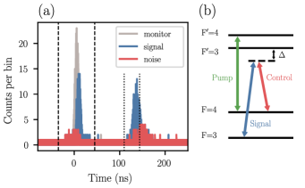
We start the experimental sequence by pumping the atoms in the ground state with a -long pulse resonant with the transition and a power of . After waiting for the pump AOM to switch off completely, we send the write-in control pulse, centered at , to the memory. To ensure optimal temporal overlap between the signal and the write-in control pulse, the signal pulse is delayed with respect to the write-in control pulse by the time . The FWHM of the Gaussian shaped signal pulses are set to to match the expected bandwidth of the SPDC photon source we want to couple to the memory in the near future Mottola et al. (2020). A read-out control pulse is sent into the memory after a storage time to retrieve the stored excitation. A photon arrival histogram as shown in figure 2 is recorded with an integration time of , a bin width of and a sequence repetition rate, . We denote as the sum over all counts of the monitor APD within a detection window of around , depicted as dashed line in figure 2. is defined as the sum over all counts of the signal APD within a detection window of to depicted as dotted line. We choose these limits as a good compromise between high efficiency and SNR. The noise counts are measured with the same procedure but with the mean input photon number set to .
The mean input photon number , the memory end-to-end efficiency , and the signal-to-noise ratio are then derived from the histogram. We note that the memory efficiency is slightly underestimated because the detection window for the input pulse is larger than that for the stored pulse. Additionally, the measured memory efficiency with WCS matches that with bright pulses, indicating the absence of input-intensity-dependent nonlinear effects.
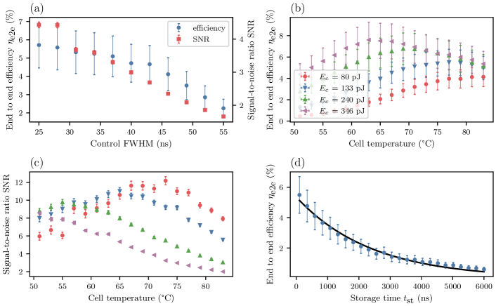
To avoid fluorescent noise Esguerra et al. (2023), we choose to operate the memory outside the Doppler linewidth of the transition and set the detuning to , a value that was found to be close to optimal in previous experiments Esguerra et al. (2023). Operation at larger detunings would require higher optical power of the control pulse to reach the same efficiency Reim et al. (2011). We use Gaussian-shaped control pulses with their FWHM, timing and peak power being the only tunable parameters. However, higher efficiencies could potentially be reached using one of the different techniques of finding the optimal control pulse shape, including iterative pulse shaping Novikova et al. (2007), machine learning Robertson et al. (2024); Lei et al. (2024) and the calculation of an optimal control field for a given signal pulse shape Phillips et al. (2008); Guo et al. (2019). Figure 3 (a) shows the measured efficiency and SNR as a function of the control pulse’s FWHM for a constant peak power of of the Gaussian control pulses at a cell temperature of . The best efficiency and SNR are reached for the shortest control pulses, suggesting that the speed of the pulse-shaping AOM might be limiting the memory efficiency and SNR at this cell temperature. We therefore set the control FWHM to the minimum value of . The effective optical depth (OD) of the atomic ensemble can be either tuned by changing the cell temperature or the detuning from the transition. At higher temperatures, i.e. higher OD, no clear efficiency dependency on the control FWHM is observed within the measurement range. Note that the energy of the control pulses increases with increasing FWHM and constant peak power, resulting in larger control pulse energy and a larger noise contribution to the SNR.
For the theoretical case of optimal control pulses, the memory efficiency would only depend on the OD and the energy of the control pulse Gorshkov et al. (2007). Figure 3 (b) & (c) show the measured efficiency and the inferred fidelity at as a function of the cell temperature for different control powers. Due to the correspondence between these two variables and the optimal temporal shape of the control pulse, the delay between the signal pulse and the control pulse is optimized for every measurement point. The memory efficiency peaks at a lower temperature for increasing optical power. At low OD the memory efficiency seems to be limited by optical power of the control pulses. At higher ODs the memory efficiency decreases with increasing OD and saturates for increasing pulse energies. This behaviour might be explained by time-varying AC Stark shift Ming et al. (2023) at higher optical powers, re-absorption of the signal due to imperfect overlap of signal and control beams, increased collision rate between Cs atoms Klein (2009); Wang et al. (2022) or a non-optimal control pulse shape Guo et al. (2019). The SNR peaks at a lower OD and power compared to the efficiency caused by the fast increase of noise counts with increasing control power and OD. Noise contribution may include fluorescent noise, spontaneous Raman scattering Esguerra et al. (2023) and four-wave-mixing noise Lauk et al. (2013); Thomas et al. (2019). Improving the pumping efficiency by using a pump beam that covers the entire cell or optimizing the amount of buffer gas is expected to reduce the noise. Four-wave-mixing noise could be reduced by exploiting polarization selection rules Buser et al. (2022).
For the following measurements we chose the experimental parameters summarized in Table 1 to simultaneously reach a high efficiency and SNR. Figure 3 (d) shows the memory efficiency as a function of the storage time. We fit the data with an exponential function to extract the memory lifetime and the zero time efficiency of , corresponding to a memory efficiency of . The errors correspond to one standard deviation of the fit function. We assume the lifetime to be limited by the diffusion of the atoms out of the interaction zone which could be increased by using larger beams or a higher amount of buffer gas.
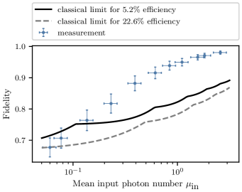
To test the quantum character of the memory, we infer the fidelity of the storage process from the achieved signal-to-noise ratio (SNR) similar to Refs. Wang et al. (2022); Thomas et al. (2023). The fidelity in this case is given by , where is the mean photon number at the input that would yield a SNR of 1 at the output Gündoğan et al. (2015); Jobez et al. (2015). We then benchmark this value against a modified fidelity threshold for WCS Specht et al. (2011); Gündoğan et al. (2012) which also takes into account the finite memory and transmission efficiencies. Figure 4 shows that the inferred fidelity in our experiments surpasses this threshold beyond when the transmission efficiency is included in the calculation. The error bars are calculated in the same way as for the previous measurements. This demonstrates that the performance of the memory cannot be mimicked by a classical measure and prepare strategy Massar and Popescu (1995) as it would inherently add excess noise Peres (2003) and therefore preclude Dieks (1982); Wootters and Zurek (1982) any high-fidelity operation. We also note that no background subtraction Leung et al. (2024) has been applied to any of these results.

IV Long duration operation in non- laboratory environment
To benchmark the robustness of the system under uncontrolled environmental conditions we moved the rack to an empty office room in the same building without any temperature and humidity control. We demonstrate the stability of the memory system by repeatedly measuring every the efficiency and fidelity over the duration of . Due to an unfortunate coincidence, the measurement took place during a time of high outside temperatures () which lead to an elevated room temperature up to which corresponds to a temperature difference of compared to the laboratory temperature. Nevertheless, memory operation could be resumed and maintained without the need for realignment. Over the duration of this measurement the average storage efficiency of () and the average input photon number of matched the laboratory performance. The wave plates (WP1 and WP2) before the polarization filtering were optimized for the specific cell operation temperature of by minimizing the noise count rate on the APD2 improving the average SNR to corresponding to a noise level of and a average fidelity of .
To investigate the memory stability performance we calculate the overlapping Allan deviation (ADEV) Riehle (2006) of the memory end-to-end-efficiency and inferred fidelity shown in figure 5 (a) out of the recorded time trace. The instability of the efficiency reaches its minimum at an averaging time of and stays below over the measurement range. For longer averaging times the instability of the efficiency and fidelity increases due to thermal fluctuations mainly causing polarization fluctuations in the optical fibers that induce power fluctuations at the memory input. figure 5 (b) shows the long-term stability of the inferred fidelity and the corresponding classical threshold. The fidelity stays mostly constant at around during the 28 hour-long measurement. The fluctuations of the classical threshold are due to small variations of the mean input photon number and the storage efficiency.
V Conclusion and outlook
We have developed a portable, rack-mounted, standalone warm vapor QM system and demonstrated its stable operation outside of a controlled laboratory environment. This represents a notable step forward, enabling quantum memory experiments in a variety of settings without the need for specialized laboratory conditions. The system’s long-term stability in non-controlled environments indicates its potential for practical applications in quantum communication. In light of recent long-range entanglement experiments Rakonjac et al. (2023); Arenskötter et al. (2023); Liu et al. (2024); Knaut et al. (2024) involving QMs, this transportable platform could enable experiments in settings without the need for access to a high-quality research laboratory. Additionally, recent advances Thomas et al. (2023, 2024); Maaß et al. (2024) towards storing single photons emitted by quantum dot sources in warm vapor QMs when combined with multimode storage capability Meßner et al. (2023) would enable the realization of enhanced quantum repeater schemes Sangouard et al. (2007); van Loock et al. (2020).
Future work will focus on miniaturizing the system Christ et al. (2024) to reduce its size for deployment on small-scale satellite platforms Oi et al. (2017). This would allow the system to be used in space-based quantum networks. In parallel, incorporating a miniaturized photon-pair source Villar et al. (2020); Mottola et al. (2020) could enable the system to function as a fully self-contained unit. Efforts will also be made to further improve storage efficiency, fidelity, and control pulse shaping Robertson et al. (2024); Lei et al. (2024), as well as reduce noise Buser et al. (2022), ensuring the system performs optimally under a range of conditions.
VI ACKNOWLEDGEMENTS
We would like to thank Lukas Heller for his support in the filter cavity design and Patrick Ledingham for discussions. We acknowledge the support from DLR through funds provided by BMWK (OPTIMO-III and QuMSeC), No. 50WM2347 and No. 50RP2090, funding by state of Berlin (application number 10206872), funding by the state of Berlin within the Pro FIT program under grant number 10206829 and by the Federal Ministry of Education and Research (BMBF) under grant number 16KISQ040K. M.G. acknowledges funding from the European Union’s Horizon 2020 research and innovation program under the Marie Skłodowska-Curie grant agreement No. 894590 (QSPACE) for the support during the early phases of this work.
References
- Lvovsky et al. (2009) A. I. Lvovsky, B. C. Sanders, and W. Tittel, Nature Photonics 3, 706 (2009).
- Lei et al. (2023) Y. Lei, F. K. Asadi, T. Zhong, A. Kuzmich, C. Simon, and M. Hosseini, Optica 10, 1511 (2023).
- Mazelanik et al. (2021) M. Mazelanik, A. Leszczyński, M. Lipka, W. Wasilewski, and M. Parniak, Quantum 5, 493 (2021).
- Barzel et al. (2024) R. Barzel, M. Gündoğan, M. Krutzik, D. Rätzel, and C. Lämmerzahl, Quantum 8, 1273 (2024).
- Nunn et al. (2013) J. Nunn, N. K. Langford, W. S. Kolthammer, T. F. M. Champion, M. R. Sprague, P. S. Michelberger, X.-M. Jin, D. G. England, and I. A. Walmsley, Phys. Rev. Lett. 110, 133601 (2013).
- Gouzien and Sangouard (2021) E. Gouzien and N. Sangouard, Phys. Rev. Lett. 127, 140503 (2021).
- Sangouard et al. (2011) N. Sangouard, C. Simon, H. de Riedmatten, and N. Gisin, Rev. Mod. Phys. 83, 33 (2011).
- Muralidharan et al. (2016) S. Muralidharan, L. Li, J. Kim, N. Lütkenhaus, M. D. Lukin, and L. Jiang, Scientific Reports 6, 20463 (2016).
- Borregaard et al. (2020) J. Borregaard, H. Pichler, T. Schröder, M. D. Lukin, P. Lodahl, and A. S. Sørensen, Phys. Rev. X 10, 021071 (2020).
- Yang et al. (2016) S.-J. Yang, X.-J. Wang, X.-H. Bao, and J.-W. Pan, Nature Photonics 10, 381 (2016).
- Distante et al. (2017) E. Distante, P. Farrera, A. Padrón-Brito, D. Paredes-Barato, G. Heinze, and H. de Riedmatten, Nature Communications 8, 14072 (2017).
- Vernaz-Gris et al. (2018) P. Vernaz-Gris, K. Huang, M. Cao, A. S. Sheremet, and J. Laurat, Nature Communications 9, 363 (2018).
- Wang et al. (2019) Y. Wang, J. Li, S. Zhang, K. Su, Y. Zhou, K. Liao, S. Du, H. Yan, and S.-L. Zhu, Nature Photonics 13, 346 (2019).
- Zhang et al. (2024) S. Zhang, J. Shi, Z. Cui, Y. Wang, Y. Wu, L. Duan, and Y. Pu, Phys. Rev. X 14, 021018 (2024).
- Gündoğan et al. (2015) M. Gündoğan, P. M. Ledingham, K. Kutluer, M. Mazzera, and H. de Riedmatten, Phys. Rev. Lett. 114, 230501 (2015).
- Jobez et al. (2015) P. Jobez, C. Laplane, N. Timoney, N. Gisin, A. Ferrier, P. Goldner, and M. Afzelius, Phys. Rev. Lett. 114, 230502 (2015).
- Stas et al. (2022) P.-J. Stas, Y. Q. Huan, B. Machielse, E. N. Knall, A. Suleymanzade, B. Pingault, M. Sutula, S. W. Ding, C. M. Knaut, D. R. Assumpcao, Y.-C. Wei, M. K. Bhaskar, R. Riedinger, D. D. Sukachev, H. Park, M. Lončar, D. S. Levonian, and M. D. Lukin, Science 378, 557 (2022).
- Ortu et al. (2022) A. Ortu, A. Holzäpfel, J. Etesse, and M. Afzelius, npj Quantum Information 8, 29 (2022).
- Zhou et al. (2023) Z.-Q. Zhou, C. Liu, C.-F. Li, G.-C. Guo, D. Oblak, M. Lei, A. Faraon, M. Mazzera, and H. de Riedmatten, Laser & Photonics Reviews 17, 2300257 (2023).
- Gündoğan et al. (2021) M. Gündoğan, J. S. Sidhu, V. Henderson, L. Mazzarella, J. Wolters, D. K. L. Oi, and M. Krutzik, npj Quant. Inf. 7, 128 (2021).
- Liorni et al. (2021) C. Liorni, H. Kampermann, and D. Bruß, New Journal of Physics 23, 053021 (2021).
- Gündoğan et al. (2021) M. Gündoğan, T. Jennewein, F. K. Asadi, E. D. Ros, E. Sağlamyürek, D. Oblak, T. Vogl, D. Rieländer, J. Sidhu, S. Grandi, L. Mazzarella, J. Wallnöfer, P. Ledingham, L. LeBlanc, M. Mazzera, M. Mohageg, J. Wolters, A. Ling, M. Atatüre, H. de Riedmatten, D. Oi, C. Simon, and M. Krutzik, “Topical white paper: A case for quantum memories in space,” (2021), arXiv:2111.09595 .
- Wallnöfer et al. (2022) J. Wallnöfer, F. Hahn, M. Gündoğan, J. S. Sidhu, F. Wiesner, N. Walk, J. Eisert, and J. Wolters, Communications Physics 5, 169 (2022).
- Gündoǧan et al. (2024) M. Gündoǧan, J. S. Sidhu, M. Krutzik, and D. K. L. Oi, Optica Quantum 2, 140 (2024).
- Reim et al. (2011) K. F. Reim, P. Michelberger, K. C. Lee, J. Nunn, N. K. Langford, and I. A. Walmsley, Phys. Rev. Lett. 107, 053603 (2011).
- Wolters et al. (2017) J. Wolters, G. Buser, A. Horsley, L. Béguin, A. Jöckel, J.-P. Jahn, R. J. Warburton, and P. Treutlein, Phys. Rev. Lett. 119, 060502 (2017).
- Kaczmarek et al. (2018) K. T. Kaczmarek, P. M. Ledingham, B. Brecht, S. E. Thomas, G. S. Thekkadath, O. Lazo-Arjona, J. H. D. Munns, E. Poem, A. Feizpour, D. J. Saunders, J. Nunn, and I. A. Walmsley, Phys. Rev. A 97, 042316 (2018).
- Finkelstein et al. (2018) R. Finkelstein, E. Poem, O. Michel, O. Lahad, and O. Firstenberg, Sci. Adv. 4, eaap8598 (2018).
- Guo et al. (2019) J. Guo, X. Feng, P. Yang, Z. Yu, L. Q. Chen, C.-H. Yuan, and W. Zhang, Nat. Commun. 10, 148 (2019).
- Wang et al. (2022) Y. Wang, A. N. Craddock, R. Sekelsky, M. Flament, and M. Namazi, Phys. Rev. Appl. 18, 044058 (2022).
- Buser et al. (2022) G. Buser, R. Mottola, B. Cotting, J. Wolters, and P. Treutlein, PRX Quantum 3, 020349 (2022).
- Thomas et al. (2023) S. Thomas, S. Sagona-Stophel, Z. Schofield, I. Walmsley, and P. Ledingham, Phys. Rev. Appl. 19, L031005 (2023).
- Esguerra et al. (2023) L. Esguerra, L. Meßner, E. Robertson, N. V. Ewald, M. Gündoğan, and J. Wolters, Phys. Rev. A 107, 042607 (2023).
- Pahl et al. (2019) J. Pahl, A. N. Dinkelaker, C. Grzeschik, J. Kluge, M. Schiemangk, A. Wicht, A. Peters, and M. Krutzik, Appl. Opt. 58, 5456 (2019).
- Snoddy et al. (2007) J. Snoddy, Y. Li, F. Ravet, and X. Bao, Appl. Opt. 46, 1482 (2007).
- Wiegand et al. (2022) B. Wiegand, B. Leykauf, R. Jördens, and M. Krutzik, Review of Scientific Instruments 93, 063001 (2022).
- Palittapongarnpim et al. (2012) P. Palittapongarnpim, A. MacRae, and A. I. Lvovsky, Review of Scientific Instruments 83, 066101 (2012).
- Heller (2023) L. Heller, Exploring quantum memory schemes in cold atoms for quantum repeaters, Phd thesis, Universitat Politècnica de Catalunya (2023).
- Mottola et al. (2020) R. Mottola, G. Buser, C. Müller, T. Kroh, A. Ahlrichs, S. Ramelow, O. Benson, P. Treutlein, and J. Wolters, Opt. Express 28, 3159 (2020).
- Novikova et al. (2007) I. Novikova, A. V. Gorshkov, D. F. Phillips, A. S. Sørensen, M. D. Lukin, and R. L. Walsworth, Phys. Rev. Lett. 98, 243602 (2007).
- Robertson et al. (2024) E. Robertson, L. Esguerra, L. Meßner, G. Gallego, and J. Wolters, Phys. Rev. Appl. 22, 024026 (2024).
- Lei et al. (2024) Y. Lei, H. An, Z. Li, and M. Hosseini, Phys. Rev. Res. 6, 033153 (2024).
- Phillips et al. (2008) N. B. Phillips, A. V. Gorshkov, and I. Novikova, Phys. Rev. A 78, 023801 (2008).
- Gorshkov et al. (2007) A. V. Gorshkov, A. André, M. D. Lukin, and A. S. Sørensen, Phys. Rev. A 76, 033805 (2007).
- Ming et al. (2023) S. Ming, J. Guo, Y. Wu, G. Bao, S. Wu, M. Shi, L. Chen, and W. Zhang, Science China Information Sciences 66, 180505 (2023).
- Klein (2009) M. J. Klein, Slow and Stored Light in Atomic Vapor Cells, Phd thesis, Harvard University (2009).
- Lauk et al. (2013) N. Lauk, C. O’Brien, and M. Fleischhauer, Phys. Rev. A 88, 013823 (2013).
- Thomas et al. (2019) S. E. Thomas, T. M. Hird, J. H. D. Munns, B. Brecht, D. J. Saunders, J. Nunn, I. A. Walmsley, and P. M. Ledingham, Phys. Rev. A 100, 033801 (2019).
- Specht et al. (2011) H. P. Specht, C. Nölleke, A. Reiserer, M. Uphoff, E. Figueroa, S. Ritter, and G. Rempe, Nature 473, 190 (2011).
- Gündoğan et al. (2012) M. Gündoğan, P. M. Ledingham, A. Almasi, M. Cristiani, and H. de Riedmatten, Phys. Rev. Lett. 108, 190504 (2012).
- Massar and Popescu (1995) S. Massar and S. Popescu, Phys. Rev. Lett. 74, 1259 (1995).
- Peres (2003) A. Peres, Fortschritte der Physik 51, 458 (2003).
- Dieks (1982) D. Dieks, Physics Letters A 92, 271 (1982).
- Wootters and Zurek (1982) W. K. Wootters and W. H. Zurek, Nature 299, 802 (1982).
- Leung et al. (2024) A. C. Leung, W. Y. S. Lau, A. D. Tranter, K. V. Paul, M. Rambach, B. C. Buchler, P. K. Lam, A. G. White, and T. J. Weinhold, APL Quantum 1, 036102 (2024).
- Riehle (2006) F. Riehle, Frequency Standards: Basics and Applications (Wiley, 2006).
- Rakonjac et al. (2023) J. V. Rakonjac, S. Grandi, S. Wengerowsky, D. Lago-Rivera, F. Appas, and H. de Riedmatten, Optica Quantum 1, 94 (2023).
- Arenskötter et al. (2023) E. Arenskötter, T. Bauer, S. Kucera, M. Bock, J. Eschner, and C. Becher, npj Quantum Information 9, 34 (2023).
- Liu et al. (2024) J.-L. Liu, X.-Y. Luo, Y. Yu, C.-Y. Wang, B. Wang, Y. Hu, J. Li, M.-Y. Zheng, B. Yao, Z. Yan, D. Teng, J.-W. Jiang, X.-B. Liu, X.-P. Xie, J. Zhang, Q.-H. Mao, X. Jiang, Q. Zhang, X.-H. Bao, and J.-W. Pan, Nature 629, 579 (2024).
- Knaut et al. (2024) C. M. Knaut, A. Suleymanzade, Y.-C. Wei, D. R. Assumpcao, P.-J. Stas, Y. Q. Huan, B. Machielse, E. N. Knall, M. Sutula, G. Baranes, N. Sinclair, C. De-Eknamkul, D. S. Levonian, M. K. Bhaskar, H. Park, M. Lončar, and M. D. Lukin, Nature 629, 573 (2024).
- Thomas et al. (2024) S. E. Thomas, L. Wagner, R. Joos, R. Sittig, C. Nawrath, P. Burdekin, I. M. de Buy Wenniger, M. J. Rasiah, T. Huber-Loyola, S. Sagona-Stophel, S. Höfling, M. Jetter, P. Michler, I. A. Walmsley, S. L. Portalupi, and P. M. Ledingham, Science Advances 10, eadi7346 (2024).
- Maaß et al. (2024) B. Maaß, N. V. Ewald, A. Barua, S. Reitzenstein, and J. Wolters, Phys. Rev. Appl. 22, 044050 (2024).
- Meßner et al. (2023) L. Meßner, E. Robertson, L. Esguerra, K. Lüdge, and J. Wolters, Opt. Express 31, 10150 (2023).
- Sangouard et al. (2007) N. Sangouard, C. Simon, J. c. v. Minář, H. Zbinden, H. de Riedmatten, and N. Gisin, Phys. Rev. A 76, 050301 (2007).
- van Loock et al. (2020) P. van Loock, W. Alt, C. Becher, O. Benson, H. Boche, C. Deppe, J. Eschner, S. Höfling, D. Meschede, P. Michler, F. Schmidt, and H. Weinfurter, Advanced Quantum Technologies 3, 1900141 (2020).
- Christ et al. (2024) M. Christ, C. Zimmermann, S. Neinert, B. Leykauf, K. Döringshoff, and M. Krutzik, Advanced Quantum Technologies , 2400076 (2024).
- Oi et al. (2017) D. K. L. Oi, A. Ling, J. A. Grieve, T. Jennewein, A. N. Dinkelaker, and M. Krutzik, Contemporary Physics 58, 25 (2017).
- Villar et al. (2020) A. Villar, A. Lohrmann, X. Bai, T. Vergoossen, R. Bedington, C. Perumangatt, H. Y. Lim, T. Islam, A. Reezwana, Z. Tang, R. Chandrasekara, S. Sachidananda, K. Durak, C. F. Wildfeuer, D. Griffin, D. K. L. Oi, and A. Ling, Optica 7, 734 (2020).