Large-area multiwavelength and polarization-insensitive metalenses via multilayer Huygens’ metasurfaces
Abstract
![[Uncaptioned image]](/html/2410.20043/assets/main_figures/graphic_abstract_render.png)
Metalenses, advanced nanostructured alternatives to conventional lenses, significantly enhance the compactness and functionality of optical systems. Despite progress in monochromatic applications, scaling metalenses to centimeter-sized apertures for broadband or multiwavelength use remains challenging due to limitations in achieving the necessary group delay (GD) with current materials. In this study, we introduce a novel multiwavelength, polarization-insensitive metalens design operating in the near-infrared (NIR). Our approach employs multiple Huygens’ metasurface layers, each optimized to modulate a specific wavelength while maintaining high transmittance and minimal phase disturbance at other wavelengths. We demonstrate a metalens operating at 2000 and 2340 nm with a numerical aperture (NA) of 0.11. In simulation, the metalens achieves a normalized modulation transfer function (MTF) that is nearly exactly diffraction-limited. The absolute focusing efficiencies are 65% and 56%, corresponding to relative efficiencies of 76% and 65% compared to an ideal lens of the same dimensions. The meta-atoms are designed using an inverse shape-optimization method that ensures polarization insensitivity and high tolerance to layer misalignment. The proposed design is compatible with large-area nanofabrication techniques, allowing metasurface layers to be fabricated individually and assembled into the final device. This innovative approach is also generalizable to any arbitrary multiwavelength phase profile beyond that of simple lensing.
I Introduction
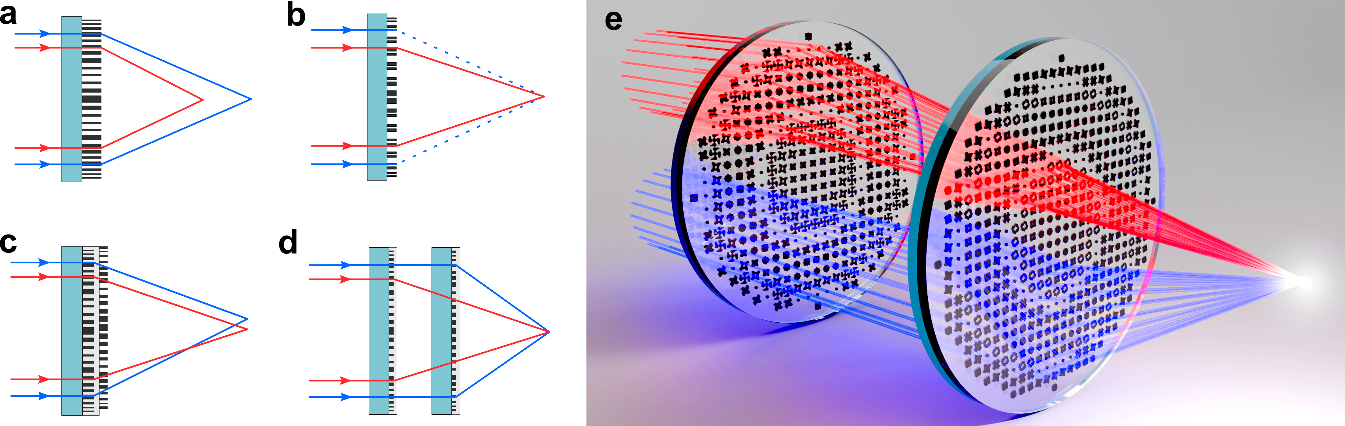
Metalenses, composed of flat arrays of subwavelength-sized scatterers known as meta-atoms, have rapidly emerged as a cutting-edge alternative to traditional diffractive and refractive lenses. By intelligently designing these scattering elements, metalenses offer unparalleled subwavelength control over the polarization, amplitude, phase, and frequency of incident light [1]. This advanced control can drastically enhance the efficiency and compactness of next-generation optical systems [2]. In the case of monochromatic operation, enormous progress has been made with high performing devices already demonstrated for many different wavelengths and up to tens of centimeters in size [3, 4, 5]. However, a major limitation in achieving these aims for broadband or multiwavelength metalenses is the difficulty in scaling to the centimeter sized apertures which are critical for practical devices. This difficulty arises because the maximum required linear phase-dispersion, or group delay (GD) that needs to be applied to an incident field for ideal achromatic focusing, is proportional to the lens diameter [6, 7]. The restricted GD values that are in practice achievable in single layer nanostructured metalenses with current dielectrics places an upper bound on the diameter, which is well below that of the centimeter sizes needed in many real-world applications (see discussion in Supplementary S-I). This leads to significant chromatic aberration as the diameter is increased (Figure 1a). To overcome this limitation, a recent study introduced the concept of a multizone dispersion-engineered metalens in which the applied GD is wrapped into discrete zones bounded by the attainable maximum value of the meta-atoms [8]. Each zone then achieves achromatic focusing independently, and phase offsets between zones are optimized such that they interfere constructively at the focal plane over the range of design wavelengths. A key limitation of this approach is that it necessitated the use of the geometric phase to independently control the phase and GD over the surface, such that the focusing response is polarization-sensitive. For systems operating with unpolarized sources, a polarization-sensitive response effectively halves the focusing efficiency and introduces unfocussed stray light, which detracts from system performance. Although a truly large-area, broadband and polarization insensitive metalens platform has yet to be demonstrated, progress has been made in the case of multiwavelength devices. Here, the GD constraint is relaxed and focusing scalable to large-areas can be achieved simply by applying a lens phase profile at each wavelength of interest utilizing an arbitrary phase-dispersion response. As most artificial sources operate at discrete wavelengths, multiwavelength rather than achromatic operation also does not significantly detract from many potential applications. Researchers have proposed several multiwavelength polarization-insensitive designs that are applicable to large-areas. These include annular interference [9, 10, 11], multilayer meta-atoms [12, 13], spatial interleaving [14, 15, 16] and multiresonant [17, 18] approaches. For the annular interference based designs, the maximum expected efficiency is low and bounded by that of an ideal binary Fresnel zone plate at 10% [9]. The multilayer meta-atom designs (Figure 1c) in simulation are able to reach above 60% focusing efficiencies for a numerical aperture (NA) of 0.2 but are heavily impacted by fabrication imperfections that vary the interlayer spacing and alignment [13]. The spatially interleaved and multiresonant designs (Figure 1b) tend to suffer from a large variation in focusing performance over the design wavelengths, with generally below 40% minimum focusing efficiency even in simulation. This effect can be attributed to a combination of unaccounted for nearfield interactions as a consequence of breaking the validity of the locally periodic approximation (LPA) and sparser spatial phase sampling at the shortest wavelengths [14, 17]. To overcome these limitations, a recent study in Ref. [19] used an advanced large-area LPA based inverse design scheme to generate red, green and blue (RGB) polarization insensitive centimeter scale visible light metalenses with almost identical focusing efficiencies over the operating wavelengths. However, the maximum achieved focusing efficiencies in simulation were still low at 24% due to the use of cross-polarization converting meta-atoms, which have characteristically lower efficiencies than isotropic meta-atom platforms.
In this work, we present a novel polarization-insensitive multiwavelength metalens design operating within the near-infrared (NIR). The design consists of multiple Huygens’ metasurface layers, where each layer modulates only a specific wavelength, while achieving high transmittance and low phase disturbance at alternative wavelengths. This approach effectively circumvents the sparse phase sampling of spatial interleaving designs and minimizes the difficulty in maintaining the validity of the LPA over a range of wavelengths simultaneously. Furthermore, as the layers are assumed to be separated by a macro-scale distance within the farfield, the approach is inherently tolerant to layer misalignment. It is also highly amenable to current large-area lithography techniques, as each layer can be fabricated as an individual metasurface chip and then simply packaged together in the final device. As proof of concept, a metalens operating at 2000 and is designed that in simulation achieves focusing efficiencies of 65% and 56% with a NA of 0.11. The operating principle, design methodology and simulated lens performance will be discussed.
II Results and discussion
II.1 Device overview and working principle
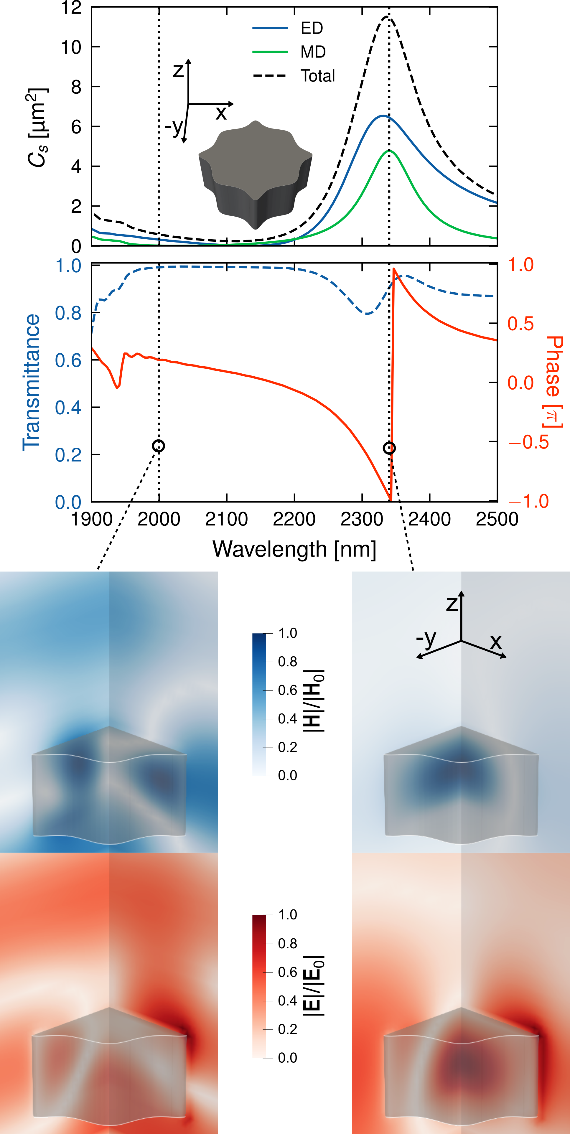
In Huygens’ metasurfaces the meta-atom array supports local spectrally overlapping electric (ED) and magnetic (MD) dipolar resonances which interfere to produce directional forward scattering and 2 phase coverage [20, 21]. The archetypal meta-atom consists of a low aspect-ratio disc, where the spectral position of the resonances and thus the phase of the transmitted field is controlled by varying the disc radius. To achieve multiwavelength functionality within this regime, we leverage two characteristics of this interaction. The first is that within the immediate spectral vicinity of the resonance, the scattering cross-section is low and the transmittance high. This is because the dipolar resonances are of the lowest order, such that no other Mie-resonances are supported in the structure within some local bandwidth. This is illustrated in Figure 2 in which the multipole decomposition, of an example meta-atom is shown, along with the field profiles at the operating wavelengths. The second is that away from resonance, the field is not strongly localized within the meta-atom (see inset field profiles in Figure 2) and does not strongly feel its geometry. Here, the metasurface behaves more like a thin-film with a small linear phase dispersion. Taken together, these traits enable Huygens’ metasurfaces which simultaneously provide 2 phase coverage at the resonance wavelength, while restricting the phase disturbance away from resonance. This is done primarily by decoupling the meta-atom array fill-factor from the spectral position of the resonances. Under this condition, it is possible for the phase accumulated off-resonance (dominated by a thin-film like interaction) to remain approximately constant over a meta-atom library. Unfortunately, the well known Huygens’ disc geometry is not ideal in this instance as it requires the array fill-factor to be proportional to the applied resonant phase due to the only geometric degree of freedom being the disc radius. To overcome this, we generate meta-atom libraries using an inverse design scheme which enables many more geometric degrees of freedom while maintaining rotational symmetry and polarization insensitive operation. Using the obtained libraries, each layer in the multilayer metalens then applies a lensing phase profile with a focal length to the wavelength , given by
| (1) |
where is the radial distance from the lens center, and represents a wavelength dependent constant that contains the phase accumulated through the alternate layers. A schematic and render of the final multilayer device focusing two wavelengths is given in Figure 1.
II.2 Inverse design of multiwavelength meta-atom libraries
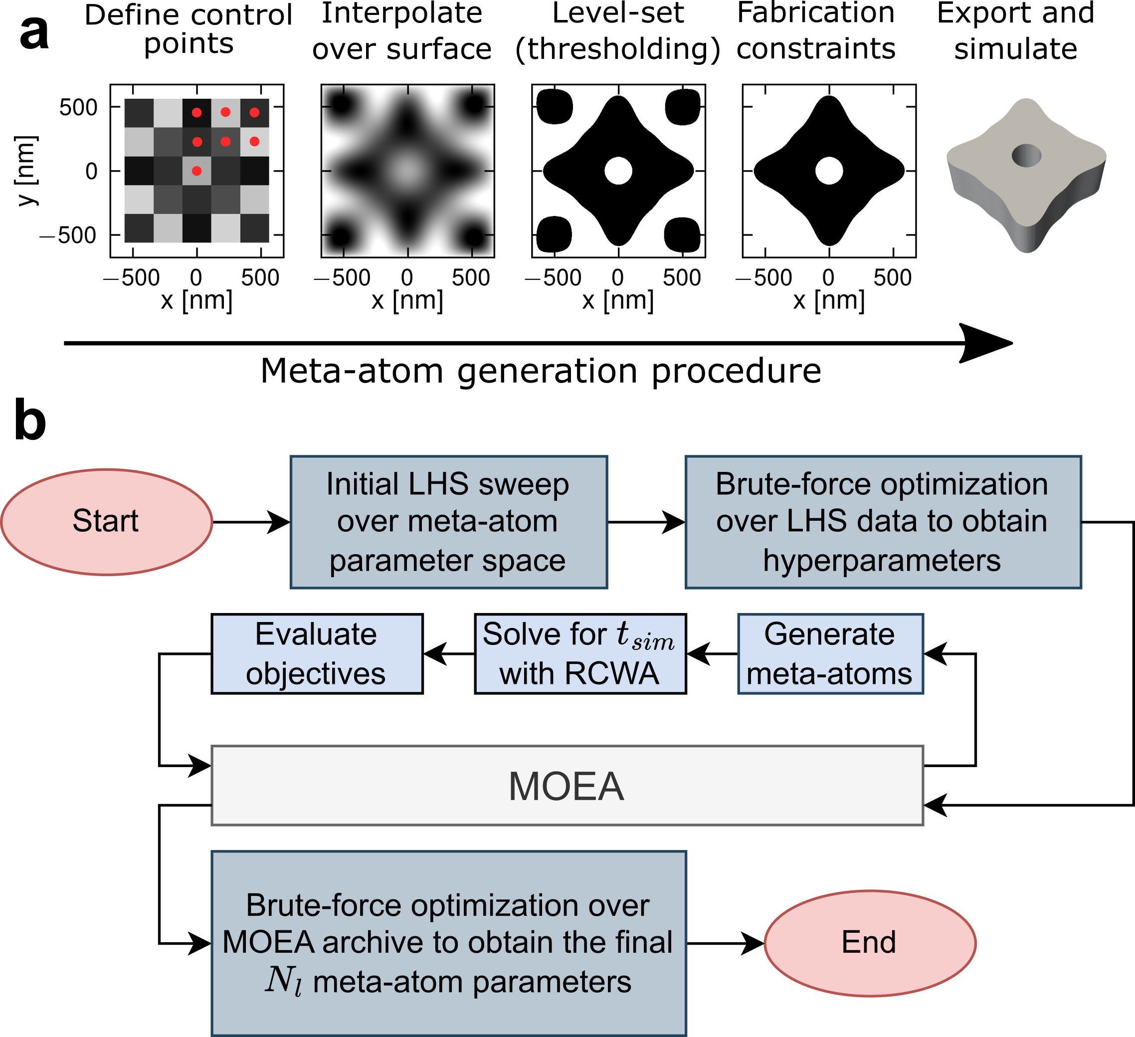
To generate the multiwavelength libraries, we use a shape optimization inverse design scheme within the LPA, which is based off the work by Whiting et al. in Ref. [22]. The core of this scheme is an efficient meta-atom parameterization method (see Figure 3a) in which the meta-atom geometry is obtained by interpolating an array of control points over the period to form a control surface. A level-set operation on this surface is then used to define the meta-atom boundary. This is a highly flexible method that allows arbitrary symmetries, and is ideal for creating polarization insensitive meta-atoms. Further fabrication constraints are imposed after obtaining the geometry through morphological or other algorithmic operations. The meta-atoms are simulated using Rigorous Coupled Wave Analysis (RCWA) at the wavelengths of interest. The complex transmittance () obtained from RCWA is then used to construct a multiobjective function quantifying the meta-atom performance (for further details, see Supplementary S-III). The constructed objectives consider the desired multiwavelength performance both at the operating wavelengths and within to avoid strong frequency dependence in the final designs, as this increases sensitivity to fabrication defects. The multiwavelength libraries are then generated by using the meta-atom control point array as optimization parameters within a gradient free multiobjective evolutionary algorithm (MOEA) [23]. This allows for a whole spanning library to be produced within a single optimization run containing roughly, 8000 objective evaluations. Further explanation of how a multiobjective optimization enables this process is available in Supplementary text. To speed up the MOEA optimization step, we first define meta-atom hyperparameters (the array period, height and non-resonant wavelength target phase) via a simple grid search based optimization using Latin Hypercube Sampling (LHS) [24] to obtain the initial dataset. The final libraries are then generated using an additional grid search over the whole MOEA archive. This is because at the end of the MOEA optimization, there are solutions spanning the entire modulation wavelength phase space, and only a subset of these that corresponds to the target modulation library phase levels are needed. Details on the benefits of selecting this discrete number for modulation phase levels are given in Section II.3 and within the Supplementary text. The algorithm flowchart of this process is shown in Figure 3b. Together with the first LHS step, a library is generated in roughly 10,000 total objective evaluations. As here we use the LPA, the simulation domain only consists of a single meta-atom unitcell. Combined with an efficient RCWA solver, this enables the whole optimization to be run on a workstation PC within one or two days.
II.3 Meta-atom library performance
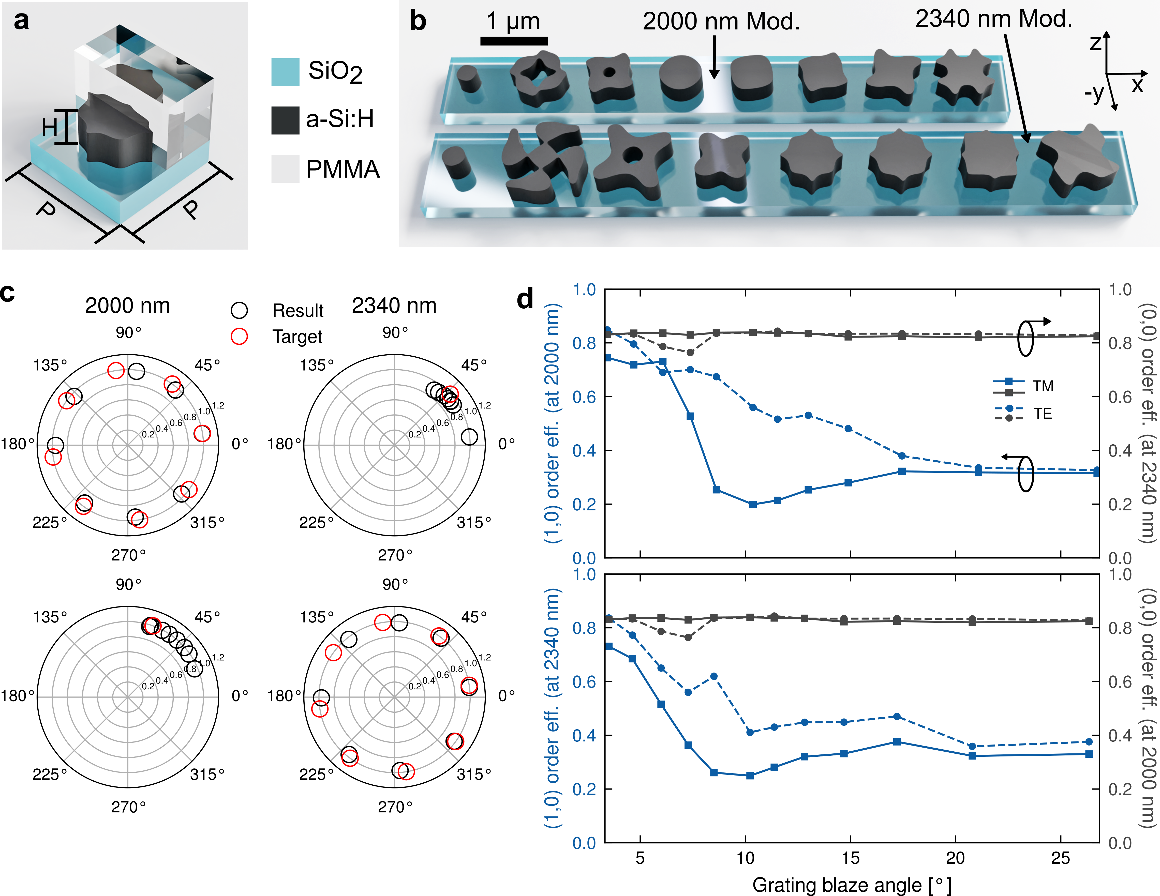
The designed meta-atom unitcells consist of a structured hydrogenated amorphous silicon (a-Si:H) layer on a fused silica (SiO2) substrate embedded in a polymethyl methacrylate (PMMA) cladding (Figure 4a). The inverse design scheme is used to generate meta-atom libraries that structure the resonant wavelength with phase levels. Using discrete rather than continuous phase levels at first seems counter-intuitive, as the geometry incurs rapid transitions over the surface that may cause the LPA to become invalid. However, we find in numerical studies that firstly the performance loss solely due to phase level discretization (known as phase quantization error in diffractive optics [25]) is less than 5% (see discussion in S-II and Figure S1b), a result which is consistent even to high NAs as 8 phase levels is far from the Nyquist condition and well samples any periodic [0,] phase function. Secondly, in numerical trials of a Huygens’ disc meta-atom geometry the difference between continuous phase levels and an 8 level library is negligible when analyzed as a blazed metagrating (Figure S2c), and is not expected to make a significant impact on the final metalens. The benefit of this approach is that it improves the off-resonant performance. Firstly, the complexity of optimizing a smaller subset of geometries for multiwavelength performance is reduced, which enables the phase deviation off-resonance to be lower. Secondly, the discrete number of meta-atom geometries minimizes the potential for off-resonance spatial phase gradients to occur, which would lead to unwanted deflection. To scale renders of the final libraries to modulate 2000 and are provided in Figure 4b. Although the geometries have complex shapes, the fabrication constraints applied during the inverse design loop restricts the minimum feature size to be larger than . Performing multipole decomposition on the meta-atoms (see Figure S4), we find that the inverse design algorithm maintains the Huygens’ resonance condition for all geometries, apart from the first two meta-atoms (counting from the left in Figure 4b) in each of the two libraries. This highlights the benefit of using an algorithmic design approach as although the Huygens’ resonance provides phase coverage for the majority of the meta-atoms it is unsurprising that for low absolute phase (measured relative to the unitcell absent the a-Si:H layer) a non-resonant geometry presents a better solution to the multiwavelength objective function. The polar plots in Figure 4c show the values of the libraries compared to the target ideal library, which is used in the final step of the optimization procedure. The results show excellent on resonance phase coverage, with a small phase range for the off-resonant wavelengths and high transmittance for both cases. The libraries were also simulated as blazed metagratings using finite difference time domain (FDTD) to ascertain their multiwavelength beam deflection efficiency in an approximation of how they would perform locally within the metalens (Figure 4d). At the resonance wavelength, both libraries show high efficiency polarization-insensitive beam deflection into the (1,0) blaze order, for angles less than , with significant performance degradation as the angle increases. This poor performance at high deflection angles is a known limitation of Huygens’ metasurfaces designed within the LPA and has been discussed in detail in Refs. [26, 27]. Here we attribute it to unaccounted for cross-talk due to the broken periodicity in the metagrating, as well as the angular dispersion of the ED and MD Mie-modes [26] in addition to the emergence of other asymmetric modes at large in plane k-vectors which interfere with the Huygens’ dipolar resonances [27]. This limits the performance of high NA Huygens’ metalenses designed using the LPA. Nevertheless, it should be noted that the 0.11 NA multiwavelength metalens presented in this work, has more than an order of magnitude higher NA than what would be achievable at centimeter scale diameters using standard single layer dispersion-engineering approaches that are limited by the restricted GD of current dielectrics (see further discussion in Supplementary S-I) [6, 7]. Furthermore, the metalens NA could be significantly increased under the same multilayer Huygens’ metasurface paradigm via the use of a more sophisticated optimization scheme which goes beyond the simple LPA. It has been shown in Ref. [26] that the Huygens’ resonance regime in nanodiscs can be implemented at larger deflection angles via judicious design of the disc aspect-ratio. This implies the angular bandwidth limitation is primarily a consequence of the LPA design method (in which only normally orientated 0th order S-parameters are considered) rather than the meta-atom platform itself. In addition, in Ref. [28] the authors used a gradient free optimization scheme on hundreds of Mie-resonant nanodiscs to produce a 0.51 NA diameter cylindrical lens with a 60% experimental focusing efficiency - thus demonstrating the potential of such a method. The trade-off being the increased computational overhead. Off-resonance, the multiwavelength libraries both have polarization-insensitive 83% efficiency into the (0,0) order, which is independent of the blaze angle indicating the strong decoupling between the on and off-resonant wavefront shaping. The reduction from unitary (0,0) transmission is due to some scattering into higher orders, as the phase-restriction is not perfect.
II.4 Whole metalens numerical simulation and analysis
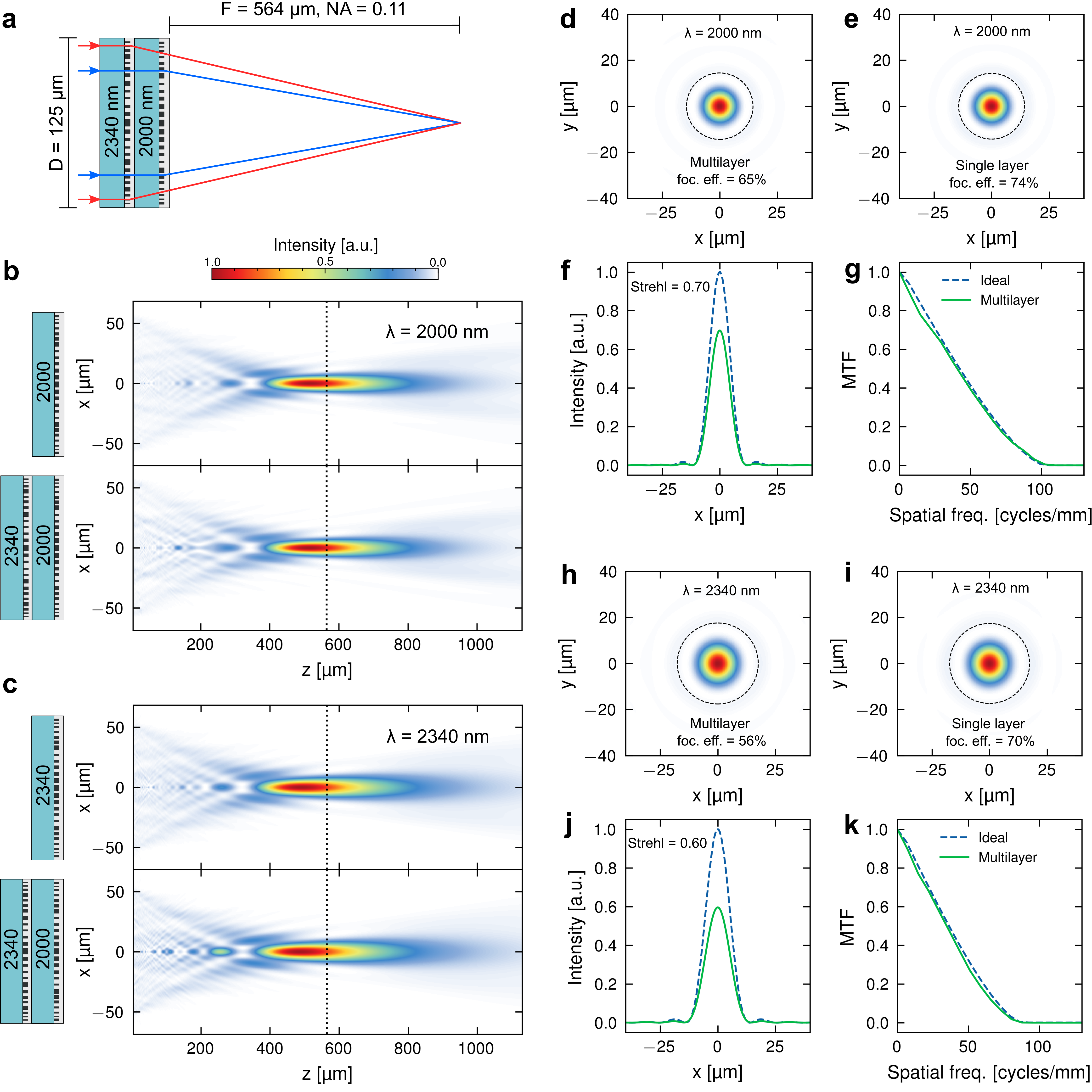
To characterize the multiwavelength metalens performance, the 8-level meta-atom libraries were used to generate two metasurfaces where each applies the hyperbolic phase in Eq. 1 to its resonant wavelength determined by a simple phase look-up table. To remain within the optimal angular bandwidth of the meta-atom libraries, we use a lens phase profile with a NA of 0.11. The multilayer device was then simulated in FDTD. Due to limited computational resources, the metalens diameter was selected to be . A schematic of the simulated structure is provided in Figure 5a. As the metalens layers are assumed to be spaced by a distance within the farfield, to avoid interlayer coupling effects whilst remaining within the computational budget, each layer was simulated individually with the field above the first layer used as the excitation source for the second layer. Further simulation details are available in the Supplementary text S-VII. In Figures 5b and c we compare the farfields of the full multilayer metalens to that of a single layer to demonstrate the effectiveness of this approach to decouple the on and off-resonant wavefront shaping. Both farfields demonstrate clear lensing with negligible change between their focal lengths, indicating the off-resonant response of the layers does not significantly disturb the applied resonant phase profile. The main distinction is the presence of increased intensity maxima closer to the lens. This results from a diffractive effect of the off-resonant layers that have a slight phase variation. They impose a weak radial periodicity over the lens’s Fresnel zones, leading to scattering into higher orders. The point spread functions (PSFs) at the focal plane are plotted in Figures 5d,e,h and i for both the single and multilayer cases. These show a highly symmetric PSF, which due to the rotational symmetry of both the meta-atoms and full metalens array, is indicative of highly polarization-insensitive focusing. The shape of the PSF for both wavelengths is also essentially identical between the single and full multilayer device. The main difference is a reduction in focusing efficiency. This is defined using the commonly adopted approach as the ratio of optical power through an aperture with a diameter three times the PSF’s full-width half maximum (FWHM) to the total power incident on the lens [19, 29, 13, 17] (dashed black circles in Figure 5). This reduction in the efficiency is also attributed to the off-resonant diffraction. Nonetheless, the multilayer device still achieves high-efficiency polarization-insensitive focusing at 65% and 56% respectively, for the 2000 and incident fields. It should also be noted that due to the restricted metalens diameter of , diffraction limited focusing through an ideal lens at this NA has a maximum focusing efficiency of 86% (see Supplementary text S-VI and Figure S6), such that the relative focusing efficiencies of the lens are 76% and 65%. Furthermore, larger centimeter-scale metalenses are expected to have improved performance as diffraction effects are reduced and the array size increases such that the LPA becomes more accurate for increasing lens area. In Figures 5f,g,j and k the one-dimensional (1D) PSF’s along the x-axis are compared to that of an ideal lens, along with the 1D modulation transfer function (MTF). Here, the MTF is calculated from the Fourier transform of the PSF via [30]:
| (2) |
where and are the spatial frequencies along the and axes. The ideal PSF used in the comparison is taken from the numerically propagated ideal lens farfield, as described in the Supplementary. These results show near diffraction-limited focusing performance, with the MTF matching almost exactly that of the ideal lens for both wavelengths. We find that the multilayer metalens in simulation produces close to ideal focusing performance, with the primary detraction simply being a reduction in the overall efficiency.
III Conclusion
We have presented a novel multiwavelength and polarization-insensitive metalens design which is suitable for centimeter scale lens diameters. In simulation, the design achieves a near diffraction-limited MTF with absolute focusing efficiencies of 65% and 56% at operating wavelengths of and for a NA of 0.11. Compared to an ideal lens of the same dimensions and NA this is equivalent to a relative focusing efficiency of 76% and 65% respectively. The design consists of multiple Huygens’ metasurface layers, where each layer structures the wavefront at the Huygens’ resonance wavelength, while decoupling the wavefront shaping off-resonance. The layers are formed from meta-atom libraries with 8 phase levels, generated via an efficient shape-optimization inverse design method that maintains the rotational symmetry of the meta-atom geometry, thus ensuring polarization-insensitive operation. A key benefit of the approach is that the layers are designed to be separated by a distance within the farfield. This allows the multilayer design to be highly tolerant to layer misalignment. Additionally, it is well suited for current large-area nanofabrication techniques, as each layer can be fabricated individually and simply packaged together in the final device. In future work, the inverse design scheme presented here can be extended to consider multiple meta-atom interactions and larger operation angles, which can be used to further increase the efficiency and NA of this approach. Furthermore, the approach presented here is highly generalizable to any arbitrary multiwavelength phase profile beyond that of simple lensing. We anticipate that it will facilitate a variety of compact, large-area, multifunctional polarization-insensitive devices, such as color routers, vortex beams, double-helix PSFs, and other advanced phase mask engineering techniques.
IV Methods
Shape-optimization inverse design
The inverse design workflow was implemented in Python using standard scientific packages NumPy and SciPy. Fabrication constraint algorithms made use of the OpenCV module to access morphological operations. To generate 3D STL models for simulation in external software the open source software OpenSCAD was used and accessed via the SolidPython module. The MOEA algorithm used was the Python implementation of Borg [23].
Numerical simulations
The inverse design optimization made use of a RCWA solver implemented in Python based on the grcwa package presented in Ref. [31]. Here, as we use a gradient free optimization, grcwa was modified to utilize an efficient JIT compiled backend via Numba. The RCWA simulations were run using 300 Fourier orders, which would take roughly for an evaluation at a single wavelength on a standard workstation PC. The complex permittivity for the RCWA simulations were extrapolated from experimental ellipsometric data (see Supplementary text S-VIII for more details).
The metagrating and large metalens simulations were performed using commercial FDTD software, Lumerical. The material optical properties were imported from the experimental ellipsometry data. For the metagrating simulations, the domain used Bloch-periodic boundary conditions in the x and y-directions with PML boundaries in the z-direction. They were excited with a normally incident plane wave source. Further details on the metalens simulations are available in the Supplementary text.
Acknowledgements
The project on which this report is based was funded by the German Federal Ministry of Education and Research (BMBF) under the funding code 01QE2004B through the Eurostars programme (Project: E!113720 MuGasMeta) and the Australian Research Council (CE200100010). Responsibility for the content of this publication lies with the author. This work was also funded by the Deutsche Forschungsgemeinschaft (DFG, German Research Foundation) through the International Research Training Group (IRTG) 2675 “Meta-ACTIVE,” project number 437527638.
References
- Neshev and Miroshnichenko [2023] D. N. Neshev and A. E. Miroshnichenko, Enabling smart vision with metasurfaces, Nature Photonics 17, 1 (2023).
- Kuznetsov et al. [2024] A. I. Kuznetsov, M. L. Brongersma, J. Yao, M. K. Chen, U. Levy, D. P. Tsai, N. I. Zheludev, A. Faraon, A. Arbabi, N. Yu, D. Chanda, K. B. Crozier, A. V. Kildishev, H. Wang, J. K. W. Yang, J. G. Valentine, P. Genevet, J. A. Fan, O. D. Miller, A. Majumdar, J. E. Fröch, D. Brady, F. Heide, A. Veeraraghavan, N. Engheta, A. Alù, A. Polman, H. A. Atwater, P. Thureja, R. Paniagua-Dominguez, S. T. Ha, A. I. Barreda, J. A. Schuller, I. Staude, G. Grinblat, Y. Kivshar, S. Peana, S. F. Yelin, A. Senichev, V. M. Shalaev, S. Saha, A. Boltasseva, J. Rho, D. K. Oh, J. Kim, J. Park, R. Devlin, and R. A. Pala, Roadmap for Optical Metasurfaces, ACS Photonics 10.1021/acsphotonics.3c00457 (2024).
- Kim et al. [2023] J. Kim, J. Seong, W. Kim, G.-Y. Lee, S. Kim, H. Kim, S.-W. Moon, D. K. Oh, Y. Yang, J. Park, J. Jang, Y. Kim, M. Jeong, C. Park, H. Choi, G. Jeon, K.-i. Lee, D. H. Yoon, N. Park, B. Lee, H. Lee, and J. Rho, Scalable manufacturing of high-index atomic layer–polymer hybrid metasurfaces for metaphotonics in the visible, Nature Materials 22, 474 (2023).
- She et al. [2018] A. She, S. Zhang, S. Shian, D. R. Clarke, and F. Capasso, Large area metalenses: Design, characterization, and mass manufacturing, Optics Express 26, 1573 (2018).
- Park et al. [2022] J.-S. Park, S. W. Daniel Lim, M. Ossiander, Z. Li, A. Amirzhan, and F. Capasso, All-Glass, Mass-Producible, Large-Diameter Metalens at Visible Wavelength for 100 mm Aperture Optics and Beyond, in 2022 Conference on Lasers and Electro-Optics (CLEO) (2022) pp. 1–2.
- Presutti and Monticone [2020] F. Presutti and F. Monticone, Focusing on bandwidth: Achromatic metalens limits, Optica 7, 624 (2020).
- Engelberg and Levy [2021] J. Engelberg and U. Levy, Achromatic flat lens performance limits, Optica 8, 834 (2021).
- Li et al. [2021] Z. Li, P. Lin, Y.-W. Huang, J.-S. Park, W. T. Chen, Z. Shi, C.-W. Qiu, J.-X. Cheng, and F. Capasso, Meta-optics achieves RGB-achromatic focusing for virtual reality, Science Advances 7, eabe4458 (2021).
- Cai et al. [2019] H. Cai, D. Czaplewski, K. Ogando, A. Martinson, D. Gosztola, L. Stan, and D. López, Ultrathin transmissive metasurfaces for multi-wavelength optics in the visible, Applied Physics Letters 114, 071106 (2019).
- Wang et al. [2021] J. Wang, J. Yang, and G. Kang, Achromatic focusing effect of metasurface-based binary phase Fresnel zone plate, Physics Letters A 407, 127463 (2021).
- Avayu et al. [2017] O. Avayu, E. Almeida, Y. Prior, and T. Ellenbogen, Composite functional metasurfaces for multispectral achromatic optics, Nature Communications 8, 14992 (2017).
- Feng et al. [2022] W. Feng, J. Zhang, Q. Wu, A. Martins, Q. Sun, Z. Liu, Y. Long, E. R. Martins, J. Li, and H. Liang, RGB Achromatic Metalens Doublet for Digital Imaging, Nano Letters 22, 3969 (2022).
- Zhou et al. [2018] Y. Zhou, I. I. Kravchenko, H. Wang, J. R. Nolen, G. Gu, and J. Valentine, Multilayer Noninteracting Dielectric Metasurfaces for Multiwavelength Metaoptics, Nano Letters 18, 7529 (2018).
- Baek et al. [2022] S. Baek, J. Kim, Y. Kim, W. S. Cho, T. Badloe, S.-W. Moon, J. Rho, and J.-L. Lee, High numerical aperture RGB achromatic metalens in the visible, Photonics Research 10, B30 (2022).
- Baek et al. [2021] S. Baek, J. Y. Park, and J.-L. Lee, Multiwavelength metalens by spatial multiplexing at visible wavelengths, Journal of Optics 23, 075102 (2021).
- Arbabi et al. [2016a] E. Arbabi, A. Arbabi, S. M. Kamali, Y. Horie, and A. Faraon, Multiwavelength metasurfaces through spatial multiplexing, Scientific Reports 6, 32803 (2016a).
- Arbabi et al. [2016b] E. Arbabi, A. Arbabi, S. M. Kamali, Y. Horie, and A. Faraon, Multiwavelength polarization-insensitive lenses based on dielectric metasurfaces with meta-molecules, Optica 3, 628 (2016b).
- Shi et al. [2018] Z. Shi, M. Khorasaninejad, Y.-W. Huang, C. Roques-Carmes, A. Y. Zhu, W. T. Chen, V. Sanjeev, Z.-W. Ding, M. Tamagnone, K. Chaudhary, R. C. Devlin, C.-W. Qiu, and F. Capasso, Single-Layer Metasurface with Controllable Multiwavelength Functions, Nano Letters 18, 2420 (2018).
- Li et al. [2022] Z. Li, R. Pestourie, J.-S. Park, Y.-W. Huang, S. G. Johnson, and F. Capasso, Inverse design enables large-scale high-performance meta-optics reshaping virtual reality, Nature Communications 13, 2409 (2022).
- Staude et al. [2013] I. Staude, A. E. Miroshnichenko, M. Decker, N. T. Fofang, S. Liu, E. Gonzales, J. Dominguez, T. S. Luk, D. N. Neshev, I. Brener, and Y. Kivshar, Tailoring Directional Scattering through Magnetic and Electric Resonances in Subwavelength Silicon Nanodisks, ACS Nano 7, 7824 (2013).
- Decker et al. [2015] M. Decker, I. Staude, M. Falkner, J. Dominguez, D. N. Neshev, I. Brener, T. Pertsch, and Y. S. Kivshar, High-Efficiency Dielectric Huygens’ Surfaces, Advanced Optical Materials 3, 813 (2015).
- Whiting et al. [2020] E. B. Whiting, S. D. Campbell, L. Kang, and D. H. Werner, Meta-atom library generation via an efficient multi-objective shape optimization method, Optics Express 28, 24229 (2020).
- Hadka and Reed [2013] D. Hadka and P. Reed, Borg: An Auto-Adaptive Many-Objective Evolutionary Computing Framework, Evolutionary Computation 21, 231 (2013).
- Bischl et al. [2023] B. Bischl, M. Binder, M. Lang, T. Pielok, J. Richter, S. Coors, J. Thomas, T. Ullmann, M. Becker, A.-L. Boulesteix, D. Deng, and M. Lindauer, Hyperparameter optimization: Foundations, algorithms, best practices, and open challenges, WIREs Data Mining and Knowledge Discovery 13, e1484 (2023).
- Soĭfer [2013] V. A. Soĭfer, ed., Computer Design of Diffractive Optics, Woodhead Publishing Series in Electronic and Optical Materials No. number 50 (Woodhead Publishing : CISP, Oxford ; Philadelphia, 2013).
- Arslan et al. [2017] D. Arslan, K. E. Chong, A. E. Miroshnichenko, D.-Y. Choi, D. N. Neshev, T. Pertsch, Y. S. Kivshar, and I. Staude, Angle-selective all-dielectric Huygens’ metasurfaces, Journal of Physics D: Applied Physics 50, 434002 (2017).
- Gigli et al. [2021] C. Gigli, Q. Li, P. Chavel, G. Leo, M. L. Brongersma, and P. Lalanne, Fundamental Limitations of Huygens’ Metasurfaces for Optical Beam Shaping, Laser & Photonics Reviews 15, 2000448 (2021).
- Cai et al. [2020] H. Cai, S. Srinivasan, D. A. Czaplewski, A. B. F. Martinson, D. J. Gosztola, L. Stan, T. Loeffler, S. K. R. S. Sankaranarayanan, and D. López, Inverse design of metasurfaces with non-local interactions, npj Computational Materials 6, 1 (2020).
- Shrestha et al. [2018] S. Shrestha, A. C. Overvig, M. Lu, A. Stein, and N. Yu, Broadband achromatic dielectric metalenses, Light: Science & Applications 7, 85 (2018).
- Goodman [2005] J. W. Goodman, Introduction to Fourier Optics, 3rd ed. (Roberts & Co, Englewood, Colo, 2005).
- Jin et al. [2020] W. Jin, W. Li, M. Orenstein, and S. Fan, Inverse Design of Lightweight Broadband Reflector for Relativistic Lightsail Propulsion, ACS Photonics 7, 2350 (2020).