SAIM: Scalable Analog Ising Machine for Solving Quadratic Binary Optimization Problems
Abstract
This paper presents a CMOS-compatible Lechner-Hauke-Zoller (LHZ)–based analog tile structure as a fundamental unit for developing scalable analog Ising machines (IMs). In the designed LHZ tile, the voltage-controlled oscillators are employed as the physical Ising spins, while for the ancillary spins, we introduce an oscillator-based circuit to emulate the constraint needed to ensure the correct functionality of the tile. We implement the proposed LHZ tile in 12nm FinFET technology using the Cadence Virtuoso. Simulation results show the proposed tile could converge to the results in about 31 ns. Also, the designed spins could operate at approximately 13 GHz.
Index Terms:
Ising Machine, Combinatorial Optimization, Analog Computing, Approximate Computing.I Introduction
The increasing complexity in computing, driven by rising demands for computational power in fields like artificial intelligence (AI) [1], and combinatorial optimization problems [2], necessitates the exploration of novel architectures. As conventional CMOS technology and architectures near their physical limits, surpassing computational limits by resorting to innovative hardware technologies and architectures becomes crucial.
Several large problems fall within the NP-complete (Non-deterministic Polynomial complete) problem class [3], for which solutions cannot be found in polynomial time [4]. As the size of these problems increases, computational energy demands increase greatly, necessitating heuristics [5] and approximations [6]. NP-complete problems can be polynomial-time reduced to one another. Therefore, if an NP-complete problem can be modeled as a physical system, we can leverage reductions from other problems to that problem and solve the resultant physical system, leading to feasible solutions [7].
In the Ising model, the arrangement of electron spins in a material’s lattice determines its magnetic properties. In this system, increasing the temperature raises the kinetic energy of the electrons, causing their spins to oscillate freely. As the temperature decreases, the kinetic energy of the electrons becomes negligible compared to their interactions with the lattice and other electrons. Like any other physical system, this system of interacting spins tends to settle in the minimum energy level, known as the ground state [8].
Each physical system can be described by the sum of its kinetic and potential energy, known as its Hamiltonian. The ground state of a system is the eigenvector to this Hamiltonian relation. Therefore, NP-complete problems are solved by mapping them to the system of interacting spins in a lattice. The minimum energy of the system provides the solution for the Ising model and the problem. A system of interacting oscillators that the Ising model can describe to solve its Hamiltonian equation is called an Ising machine (IM).
It is important to recognize that the general form of the Ising model is NP-complete, indicating that finding the exact ground state (optimal solution) for complex Ising models can be computationally challenging. While Ising formulations do not solve NP-complete problems exactly, they can still be advantageous for certain applications. Ising models, viewed as physical systems of interacting spins, often enable efficient approximate solutions, making them valuable tools for addressing many NP-complete problems. In particular, IMs excel at finding near-optimal solutions to combinatorial optimization problems in a category known as quadratic unconstrained binary optimization (QUBO) [7]. Other NP-complete problems can be addressed by mapping them to the QUBO framework. Unfortunately, the physical implementation of IMs often limits the size of QUBO problems due to the constraints imposed by available hardware graph structures.
To date, various technologies have been employed to implement IMs. These include superconductor-based IMs, which operate at 4K temperatures [9], quantum annealers, such as D-Wave Two Quantum (DW2Q) from D-Wave company, which function at mK temperatures [10], coherent IMs [11]. Cmos-compatible IMs [12, 13]. Among these implementations, the fabrication complexity of CMOS-compatible IMs is significantly lower due to the maturity of available CMOS technologies. However, similar to other technologies, scalability remains the primary challenge CMOS-compatible IMs face. The Ising machine requires all-to-all connectivity, which makes its implementation extremely challenging, and as a result, the proposed structures for CMOS-compatible IMs are not available.
To address the scalability issues and mapping QUBO problem on annealers, Lechner, Hauke, and Zoller came up with a new architecture for IMs [14]. This architecture, known as LHZ, maps the interactions of an all-to-all connected system to the local interactions of the node of a tiled system. The tile is the unit cell of the hardware, consisting of four nodes interacting with each other under a constraint known as a penalty term. Each tile interacts with its neighbors, achieving long-range interactions between nodes.
This paper will present a CMOS-compatible scalable analog Ising Machine (called SAIM), which is based on the LHZ architecture. Thus, in this work, we introduce an analog LHZ tile structure. For this structure, we provide two circuits to emulate the required spins in the LHZ tile. One is based on a modified design of a prior voltage-controlled oscillator (VCO) circuit, which will serve as the physical spins. The other is a VCO circuit structure designed to simulate the necessary ancilla spin to model the required penalty of the LHZ tile, ensuring the correct functionality of the tile. In the LHZ-based Ising machine, the circuit connections are fixed, and weights of the given problem are applied through pump signals to the physical spins. The tile is implemented on the 12nm process in Cadence Virtuoso and simulated using Cadence Spectre to verify the functionality of the proposed structure. The results show the high stability of the proposed structure.
The remainder of the paper is organized as follows. In Section II, we describe the methodology and the architecture that is used for Ising machine implementation in this work. Section III describes the analog circuit for ideal parameters and then, for example, the 12nm CMOS process. In section IV, we discuss the results from 12nm CMOS and the power needed.
II Methodology
II-A Ising Machine
An IM is a specialized annealer machine that solves combinatorial optimization problems based on the Ising model. In an IM, spins interact with each other and can be either up (1) or down (-1). The minimum energy needed by the system will be achieved under the optimal solution of the problem. The Hamiltonian equation, which gives the system’s energy, is described by
| (1) |
where represents the local field acting on spin , denotes the orientation of spin , and signifies the interaction strength between spins and .
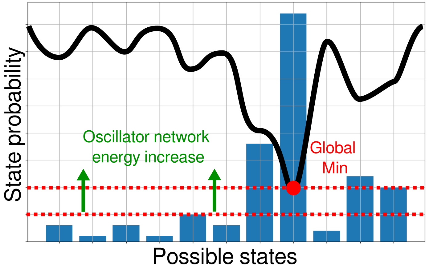
The annealing process in the IMs varies depending on the specific structure of the IM and the technology used to fabricate it. Physical annealing involves the slow cooling down of the system, which decreases the kinetic energy of the electrons to the point that the spins are not freely oscillating and settle in a state, which translates to gradient descent in the possible state space to the ground state, as shown in Fig. 1. Simulated annealing mimics this behavior by combining a greedy search method with random steps (noise) to avoid local minimus. In quantum annealers, the system is put in the ground state of an initial easy problem and then, by adiabatic annealing, moves to the hard problem’s ground state [8]. Here, as demonstrated in Fig. 1, the leaky oscillating network will gain energy until it reaches the first stable state with the smallest loss.
II-B LHZ Architecture
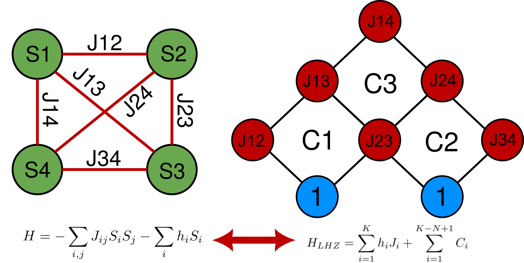
As stated, scalability is the fundamental challenge of the IM implementations. LHZ addresses this issue by converting all-to-all connectivity to two-by-two connectivity. To accommodate all interaction matrix elements, the system size in LHZ architecture is enlarged from N logical spins to physical spins.
In the LHZ architecture, each interaction between two logical spins is represented by a physical spin. Its local field demonstrates the interaction between two corresponding logical spins. Thanks to this structure, all-to-all interactions are converted to the local fields. Owing to this feature, the LHZ structure is scalable. Additionally, LHZ mapping has an additional constraint parameter , also known as a penalty term. The Hamiltonian of the LHZ is obtained by
| (2) | |||
where is the physical spin, is the local field which is generated based on in Eq.(1), and is the constraint. The number of penalty terms () is , and they are defined to guarantee that the number of positive spins in each of the tiles is always even. These constraints must be satisfied to ensure that the LHZ structure correctly models the all-to-all interactions of the IM. The penalty term is defined based on the hardware structure. In Fig. 2, the corresponding LHZ structure of a 4-node graph (e.g., 4-node Max-Cut problem) which contains 3 LHZ tiles is shown. Note that each weight value of the given QUBO () is mapped to the local field of the corresponding node of the LHZ ).
III Circuit implementation of analog LHZ tile
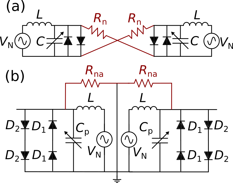
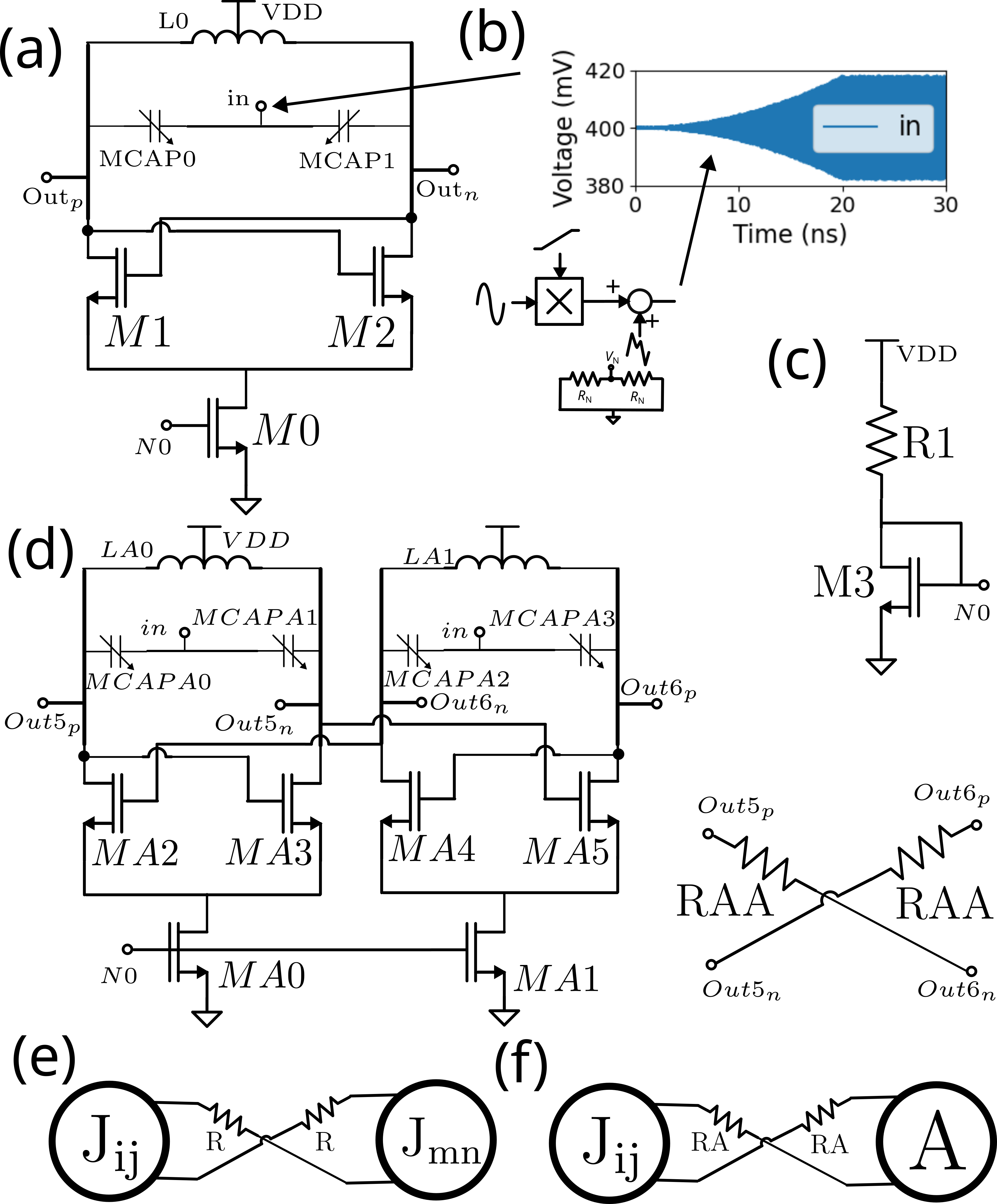
To implement the physical spins, we employ the spin structure, which has been presented in [8]. The spin circuit structure is an ideal LC oscillator. Fig. 3(a) demonstrates these spins. Since the interaction between the spins is fixed in the LHZ structure, we utilize fixed-value resistors in the antiferromagnetic (aF) scheme to make fixed negative interactions between nodes. In our design, the local fields are controlled by the electric charge pumped on the parametric capacitor, and they are changed based on the weights of the given QUBO problem. The capacitor’s charge value is described as,
| (3) |
where is the capacitor charge, , and are constants defining the pump’s amplitude and its changing rate function for annealing, respectively. is the annealing time, is the pump frequency, is the capacitor value and is capacitor’s voltage. The diodes are exploited to limit the output voltage of the LC oscillators.
To capture the LHZ conditions, we need to add the penalty function implemented via ancillary nodes. Fig. 3(b) shows the proposed ancillary circuit. The ancilla nodes should be able to generate 4, 0, or -4 kinetic energy compared to the normal nodes to fulfill the LHZ condition as explained in section II-B. The ancilla circuit contains two LC oscillators, which are connected in an aF scheme with higher interaction than other aF connections. Here, the negative output of the ancilla is grounded, and the two ports are from the positive outputs of the LC oscillators. The charge pump amplitude described by and constants in the capacitor equation of ancilla are twice their counterparts in normal nodes.
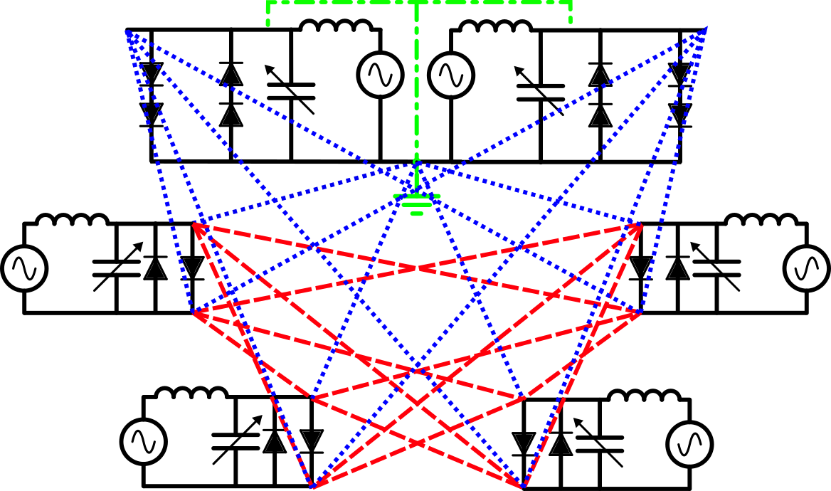
A single tile’s connections are shown in Fig. 4. Here, three different resistor values for aF connections are used: between nodes, between node and ancilla, and in the ancilla circuit. These resistors determine the limits of interactions between different nodes, and they are fixed for all the problems that we map on the IM.
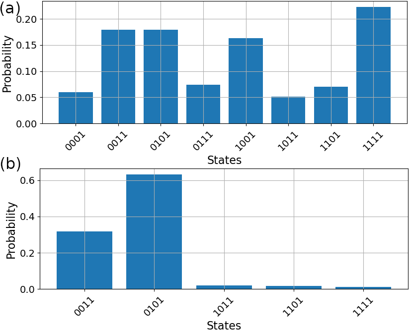
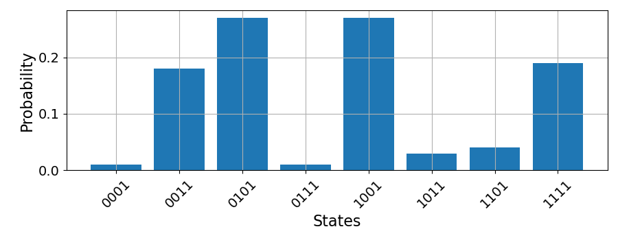
To verify this structure, we have implemented a technology-independent single LHZ tile based on the structures and values provided in Figures 3(b) and 4. Three tile structures are also employed to implement an Ising machine for solving unweighted Max-Cut (Fig. 2). The simulation results for 1000 runs on the noisy circuits are shown in Fig. 5. The simulations were done with the NgSPICE engine. We extracted the output waveform of each node and, using FFT, calculated the phase of oscillations. Since the global phase doesn’t affect the ground states, the mirror of ground states is also a valid answer. We always assume the first node is one, and based on the phase difference, we calculate the value of other nodes. Fig. 5 shows the simulation results for a (a) tile and a (b) 4-node network.
III-A Implementation on 12 nm process
After validating the design with ideal oscillators, the tile circuit of an LHZ network was implemented with 12 nm CMOS technology. The parametric oscillators are based on the discussed LC oscillators. The schematic and parameters of the four spins and an ancillary node of the LHZ tile are illustrated in Fig. 6. The oscillation frequency of a single oscillator in the target technology is \qty13.37. In Fig. 6 (a), the in terminals are injected with an annealing signal with added thermal noise shown in Fig. 6 (b). This pump signal increases quadratically with time until the annealing time is reached. Therefore, the pump signal is described as for and for , where , , and .
The thermal noise is generated from two parallel \qty10-resistors. The expression for the noise spectral density [15] is , where is the Boltzmann constant, is the temperature, and . At , the resistors generate \qty[per-mode=symbol]8.28e-20^2\per of thermal noise. These and thermal noise signals with the resistors connecting two oscillators should be optimized to ensure uniformity and a high probability of even states. The maximum oscillator amplitude is controlled by the transistors at the current source, M0 and MA0, and their channel width is controlled to ensure the LHZ conditions.
IV Results and Discussion
The proposed analog LHZ tile has been implemented in Cadence Virtuoso with 12nm technology and simulated using Cadence Spectre. The simulation result of 100 runs for a single LHZ tile is shown in Fig. 7. Here, the probability of correct states is around \qty90, and the probability distribution is relatively uniform for each possible correct state; the two facts indicate that the tile circuit is suitable for an LHZ IM. This design takes about \qty31 to reach its final state. The transients depicted in Fig. 8 are the voltage waveforms at the four physical spins (i.e., Spin 1 to 4) and two internal spins of the ancillary node (Spin 5 and 6). The waveforms are normalized to the Spin 1’s amplitude. Fig. 8 (a) shows one possible minimum-energy state: all of the four nodes in an LHZ tile are in-phase and out of phase with the two ancillary nodes. Fig. 8 (b) shows another least-energy configuration where two LHZ spins in-phase and two out of phase, and the sum of ancillary nodes’ energy near zero, resulting in a ground state.
The main benefits of IM in solving QUBO problems compared to the classical machines are its faster response time and lower energy consumption per problem. We used the same example described in [16], a MaxCut problem for a graph with 100 nodes and a degree of three, for energy consumption comparison. In our design, the power consumption is computed based on the number of tiles needed for certain problems. The simulated results in [17] imply that the time to reach a low-energy state and stabilize does not scale significantly with the problem size. Our analytical studies show the inference time of the system for 100 nodes MaxCut problem will be around \qty100. With the above conditions, obtaining a solution to that problem for our design consumes about \qty2.91 energy. The corresponding energy-time product is \qty2.91e-13⋅, which is comparable with the best result reported in [16]. Two techniques can be employed to reduce the circuit power consumption. First, since the problem graph is not fully connected and the non-ancillary nodes in an LHZ architecture represent its edges, only a few of them should be powered on while all ancillary nodes are still active. Second, reducing the bias current and, as a result, oscillating amplitudes at each node will save power drastically, improving the energy per problem.
Finally, we should emphasize that the main factors in energy consumption are power and time-to-solution. Digital annealing processors feature low power consumption but take much longer to settle in the ground state. For example, the design [18] consumes \qty35.2 at \qty10 yet it takes 10,000 steps to solve a 512-node Max-cut problem. On the other hand, analog implementations solve such problems significantly faster but with a higher power consumption. For instance, [16] report a 100-node Max-cut solver with \qty64.64 time-to-solution and \qty75 average power consumption. Our proposed method is also an analog implementation and has a high power consumption of 5mW per tile. However, the fast time to solution makes it more energy efficient compared to other designs.
V Conclusion
The LHZ-based Ising machine promises an efficient solution for NP-complete problems with a scalable architecture. We have proposed the basic element (i.e., tile) of an analog LHZ Ising machine with an acceptable accuracy that can be utilized in a conventional CMOS process. To guarantee the correct functionality of the LHZ tile, we suggested a circuit implementation for the ancillary node. We implemented the proposed analog tile in 12nm technology and verified its functionality and stability. The tile stabilizes at 31ns and consumes 6mW power.
References
- [1] R. Desislavov, F. Martínez-Plumed, and J. Hernández-Orallo, “Trends in AI inference energy consumption: Beyond the performance-vs-parameter laws of deep learning,” Sustainable Computing: Informatics and Systems, vol. 38, p. 100857, 2023.
- [2] X. Yang, Z. Wang, H. Zhang, N. Ma, N. Yang, H. Liu, H. Zhang, and L. Yang, “A review: machine learning for combinatorial optimization problems in energy areas,” Algorithms, vol. 15, no. 6, p. 205, 2022.
- [3] M. R. Garey, D. S. Johnson, and L. Stockmeyer, “Some simplified NP-complete problems,” in Proceedings of the Sixth Annual ACM Symposium on Theory of Computing, 1974, pp. 47–63.
- [4] R. M. Karp, “On the computational complexity of combinatorial problems,” Networks, vol. 5, no. 1, pp. 45–68, 1975.
- [5] V. Kesavan, R. Kamalakannan, R. Sudhakarapandian, and P. Sivakumar, “Heuristic and meta-heuristic algorithms for solving medium and large scale sized cellular manufacturing system NP-hard problems: A comprehensive review,” Materials Today: Proceedings, vol. 21, pp. 66–72, 2020.
- [6] D. S. Hochba, “Approximation algorithms for NP-hard problems,” ACM Sigact News, vol. 28, no. 2, pp. 40–52, 1997.
- [7] A. Lucas, “Ising formulations of many NP problems,” Frontiers in Physics, vol. 2, p. 74887, 2014.
- [8] S. K. Vadlamani, T. P. Xiao, and E. Yablonovitch, “Physics successfully implements Lagrange multiplier optimization,” Proceedings of the National Academy of Sciences, vol. 117, no. 43, pp. 26 639–26 650, 2020.
- [9] S. Razmkhah, M. Kamal, N. Yoshikawa, and M. Pedram, “Josephson parametric oscillator based ising machine,” Physical Review B, vol. 109, no. 1, p. 014511, 2024.
- [10] R. Hamerly, T. Inagaki, P. L. McMahon, D. Venturelli, A. Marandi, E. Rieffel, H. Takesue, and Y. Yamamoto, “Quantum vs. optical annealing: benchmarking the opo Ising machine and D-wave,” in CLEO: QELS Fundamental Science. Optica Publishing Group, 2018, pp. FTu4A–2.
- [11] D. Pierangeli, G. Marcucci, and C. Conti, “Large-scale photonic ising machine by spatial light modulation,” Phys. Rev. Lett., vol. 122, p. 213902, May 2019. [Online]. Available: https://link.aps.org/doi/10.1103/PhysRevLett.122.213902
- [12] C. Yoshimura, M. Hayashi, T. Takemoto, and M. Yamaoka, “CMOS annealing machine: A domain-specific architecture for combinatorial optimization problem,” in 2020 25th Asia and South Pacific Design Automation Conference (ASP-DAC), IEEE, 2020, pp. 673–678.
- [13] Y. Su, T. T.-H. Kim, and B. Kim, “Flexspin: A scalable CMOS ising machine with 256 flexible spin processing elements for solving complex combinatorial optimization problems,” I2022 IEEE International Solid- State Circuits Conference (ISSCC), vol. 65, IEEE, 2022, pp. 1–3.
- [14] W. Lechner, P. Hauke, and P. Zoller, “A quantum annealing architecture with all-to-all connectivity from local interactions,” Science Advances, vol. 1, no. 9, p. e1500838, 2015. [Online]. Available: https://www.science.org/doi/abs/10.1126/sciadv.1500838
- [15] B. Razavi, Design of Analog CMOS Integrated Circuits, 2nd ed. New York, NY: McGraw-Hill Professional, 2016.
- [16] Y. Wang and X. Fong, “Energy-efficient ising machines using capacitance-coupled latches for MAXCUT solving,” in 2024 IEEE International Symposium on Circuits and Systems (ISCAS), 2024, pp. 1–5.
- [17] T. Wang, L. Wu, P. Nobel, and J. Roychowdhury, “Solving combinatorial optimization problems using oscillator-based ising machines,” Natural Computing, vol. 20, no. 2, pp. 287–306, Jun. 2021.
- [18] T. Megumi, A. Endo, and T. Kawahara, “Scalable fully-coupled annealing processing system implementing 4096 spins using 22nm CMOS LSI,” IEEE Access, vol. 12, pp. 19 711–19 723, 2024.