Transport properties and quantum phase transitions in one-dimensional superconductor-ferromagnetic insulator heterostructures
Abstract
We theoretically propose a one-dimensional electronic nanodevice inspired in recently fabricated semiconductor-superconductor-ferromagnetic insulator (SE-SC-FMI) hybrid heterostructures, and investigate its zero-temperature transport properties. While previous related studies have primarily focused on the potential for generating topological superconductors hosting Majorana fermions, we propose an alternative application: using these hybrids to explore controllable quantum phase transitions (QPTs) detectable through transport measurements. Our study highlights two key differences from existing devices: first, the length of the FMI layer is shorter than that of the SE-SC heterostructure, introducing an inhomogeneous Zeeman interaction with significant effects on the induced Andreev bound states (ABS). Second, we focus on semiconductor nanowires with minimal or no Rashba spin-orbit interaction, allowing for the induction of spin-polarized ABS and high-spin quantum ground states. We show that the device can be tuned across spin- and fermion parity-changing QPTs by adjusting the FMI layer length orange and/or by applying a global backgate voltage, with zero-energy crossings of subgap ABS as signatures of these transitions. Our findings suggest that these effects are experimentally accessible and offer a robust platform for studying quantum phase transitions in hybrid nanowires.
I Introduction
Hybrid heterostructures combining properties of different materials have emerged as new platforms to investigate quantum phases and exotic phenomena otherwise nonexistent in nature. A prominent example are superconductor-ferromagnet (SC-FM) heterostructures [1, 2, 3, 4, 5], which combine two antagonistic states of matter: ferromagnets, where the spins of electrons tend to be aligned, and superconductors, where their microscopic constituents, the Cooper pairs, are made of electrons with anti-aligned spins. When these materials are forced to coexist at an interface, a rich phenomenology emerges, such as the spatial oscillation of superconducting correlations, the emergence of transitions in SC-FM-SC junctions, and the generation of spin-triplet superconductors [6, 7]. From the technological point of view, SC-FM hybrids represent a potential breakthrough for low-dissipation electronics.
Another example of advanced hybrid materials arises in the context of Majorana quantum wires, where semiconductor-superconductor (SE-SC) heterostructures have been fabricated to furnish a semiconductor nanowire with superconducting correlations via the proximity effect [8, 9, 10, 11, 12, 13].
According to seminal theoretical works [14, 15], a topological superconductor ground state with Majorana zero-modes localized at the ends of the device could be induced as a result of the combination of three main ingredients: a) strong Rashba spin-orbit coupling, such as that existing in InAs or GaAs semiconductor nanowires, b) proximity-induced superconductivity provided by the interface with a conventional wave superconductor (e.g., Al), and c) an externally applied magnetic field in the direction perpendicular to the spin-orbit axis.
In recent years, a novel type of one-dimensional heterostructure combining all the aforementioned materials: semiconductors, superconductors and ferromagnetic insulators (“SE-SC-FMI hybrids” for short) have been fabricated using molecular beam-epitaxy techniques [16, 17, 18]. The main goal in these works was to avoid the necessity to apply an external magnetic field in the Majorana nanowire devices, which technically constrains the device layout and is detrimental to the bulk superconductor. In these devices, the layer of FMI material (in this case, a EuS shell, see Fig. 1) generates a proximity-induced built-in Zeeman exchange field on the SE nanowire, therefore mimicking the presence of an applied external field. In this way the operation of the triple hybrid Majorana device can be greatly simplified. The experimental results of Ref. [17] has shown suggestive zero-bias conductance peaks, potentially indicating the presence of Majorana zero-modes. A number of theoretical studies [19, 20, 21, 22, 23, 24, 25, 26] have recently focused on this novel setup.
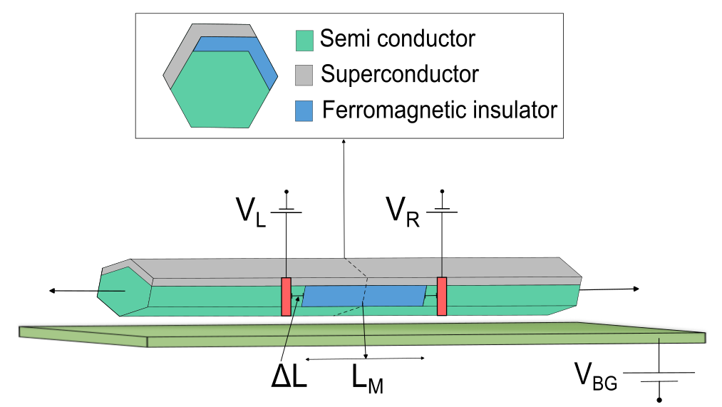
Motivated in these new developments, in this article we theoretically study the transport properties of a triple SE-SC-FMI hybrid device depicted in Fig. 1, which is inspired in (albeit different to) those studied in Refs. [16, 17, 18]. In a previous work [26], we demonstrated that this type of device is intrinsically interesting due to its complex subgap electronic structure, which arises due to the existence of spin-polarized Andreev bound states (ABS) localized at the FMI region, and predicted the occurrence of spin- and parity-changing quantum phase transitions (QPTs) as the parameter varies, where is the length of the FMI layer and is the Fermi wavelength of the semiconductor nanowire. We stress that this parameter can change either by fabricating different devices with different values of , or due to an in-situ modulation of the global chemical potential of the device using voltage gates (which effectively modifies the conduction-band filling and therefore ). In this article we complement Ref. [26] by focusing on the study of the transport properties of the device. By using an effective discrete model, we compute the transport properties at using standard non-equilibrium Keldysh Green’s functions, and show that by means of a back-gate allowing to modulate the charge of the entire SE nanowire, the QPTs could be experimentally observed in the tunneling conductance spectra . Our study is different from previous ones related to SE-SC-FMI hybrids in two crucial aspects: a) we allow the length of the FMI layer to be shorter than the length of the SC layer, effectively creating an inhomogeneous profile of Zeeman exchange interaction which greatly affects the behavior of the induced subgap ABS. The possibility to change (and control) the length of the FMI layer enables an interesting knob to study exotic quantum phases. In particular the limit allows to make an interesting connection with the physics of magnetic impurities in superconductors and the emergence of the ABS (known as Yu-Shiba-Rusinov states in this context, see Ref. [27] for a review). b) We focus on SE nanowires with weak (or no) Rashba spin-orbit coupling. While this assumption prevents us from describing topological phases in the device, the spin projection of the induced ABS becomes a good quantum number, allowing the emergence of high-spin ground states. From the experimental point of view, the realization of such device would require to use a centrosymmetric SE nanowire, such as silicon (Si), in order to minimize the Rashba coupling and to maintain as a good quantum number. The rest of the paper is organized as follows. In Sec. II, we introduce a theoretical model for a one dimensional SE-SC heterostructure with a FMI interface in a central region, including a coupling to normal leads. In Sec. III we present the details of the calculation of the conductance via non-equilibrium Keldysh Green’s functions. In Sec. IV we present results for the local and non-local conductances, and finally, in Sec. V, we provide a summary and our conclusions.
II Theoretical model
We start our theoretical description with the following discrete -site one-dimensional model Hamiltonian representing the finite central segment containing the triple SE-SC-FMI interface (see central region in Fig. 1), consisting of a single-channel SE nanowire covered by a bulk SC layer (i.e., a Al layer depicted in gray) and a coexisting finite FMI layer (i.e., EuS layer depicted in blue) of length . The Hamiltonian reads
| (1) |
where and represent the creation and annihilation fermionic operators, respectively, at site with spin projection . The parameter describes the effective hopping amplitude of electrons in the single-channel SE nanowire, the effective pairing parameter represents the proximity-induced superconducting pairing amplitude generated by the coupling with the SC layer, and corresponds to the effective Zeeman exchange interaction induced by the FMI layer. Note that we have excluded the Zeeman exchange from the sites at the ends (i.e., sites and ) in order to allow these sites to couple to the measuring contacts (see below). This situation is indeed closer to the experimental setups of Refs. [17, 18], where the measuring contacts are placed away from the FMI layer. Therefore, the actual length of the the FMI layer is represented by sites (i.e., , where is the lattice parameter).
The chemical potential is a parameter effectively representing the presence of a uniform back gate potential (see green surface in Fig. 1) acting on the entire length of the heterostructure, which modulates the overall band filling of the SE nanowire. We stress that the ability to modulate the charge in these devices has been experimentally demonstrated in a recent work [17]. As stated in Ref. [26], the relevant parameter controlling the position of the ABS in this type of device is the dimensionless product . Introducing a global background gate , we claim that the Fermi momentum can be externally controlled using the relation , therefore providing an experimentally feasible way to explore the phase diagram of the device.
The device is assumed to be weakly coupled to measuring normal leads connected to bias voltages and , introduced to study its transport properties (see Fig. 1). We assume that the measuring contact leads are described by the Hamiltonian
| (2) |
where the terms and describe, respectively, the left and right normal leads (see red finger-type structures in Fig. 1) which we describe as non-interacting semi-infinite chains
| (3) |
where , and where are the respective chemical potentials of the leads, which can be independently controlled via bias voltages and can be used to perform tunneling spectroscopy of the device. Finally, the term
| (4) |
represents the tunneling coupling, where the tunneling parameters can be independently controlled via pinch-off gates placed beneath the SE-SC-FMI structure (not shown in Fig. 1).
A crucial aspect in the theoretical study of this type of nanostructures is the fact that the localization length of the subgap ABS, , where is the Fermi velocity of the SE nanowire and is the energy of the ABS inside the gap , can greatly exceed when , introducing important finite-size effects. While in certain experimental devices such finite-size effects are a real consequence of quantum confinement, for simplicity here we have eliminated them to avoid further theoretical complexities. A basic strategy to minimize these effects consists in increasing the system size to values . However, such naïve procedure can rapidly exceed our computational capability, and therefore other approaches are needed. In this work we use Dyson’s equation to embed the finite-wire+leads system into semi-infinite one-dimensional chains located on each side of the central region (see Fig. 1), therefore reconstituting an infinite heterostructure where finite-size effects are absent. We therefore introduce the semi-infinite 1D chains representing SE-SC heterostructures (with no FMI layer)
| (5) | ||||
| (6) |
and the coupling term
| (7) |
that merges the three regions together. For simplicity, and to avoid the introduction of further inhomogeneities, identical values of and in Eqs. (1), (5), and (6) are used. This embedding procedure effectively allows us to study the effect of an inhomogeneous Zeeman field of length into an infinitely-long, and otherwise homogeneous, SE-SC heterostructure with a very low computational cost. In practice, we expect this model to be valid in the limit , where is the total length of the device. On the other hand, the positions of the leads, placed at a distance from the magnetic region, are dictated by the wavefunctions of the ABS, which localize within the magnetic region. The leads cannot be farther than the localization length of the ABS, otherwise there would be no overlap with the charge carriers in the contact zone and no current would be detected.
In our numerical calculations we have used realistic parameters in order to represent the experimental systems as close as possible. Note that the Hamiltonian Eq. (1) is to be interpreted as a coarse-grained model describing effective degrees of freedom in the SE-SC-FMI structure near the Fermi level and at low temperatures . Here, both the SC and FMI layers have been integrated out, and we are assuming that their effects are entirely described by effective parameters and respectively. In particular, the hopping , representing the effective bandwidth of the SE nanowire, is an arbitrary parameter which needs to be fitted in order to reproduce the low energy physics near . In the first place, we demand that the usual experimental situation is obeyed, and therefore set the ratio to the conservative value . Next, we have set the relation between the induced pairing parameter and the Zeeman interaction as according to the results reported in Ref. [17] for InAs-Al-EuS in hybrid nanowires. Finally, assuming that the physical superconducting coherence length induced in the NW is of the order of nm 111S. Vaitiekėnas, private comunication, and using the expression of the Fermi velocity extracted from the tight-binding model at half-filling , i.e., , we obtain the estimation for the coarse-grained lattice parameter nm. With these estimated values, the length used in Ref. [18] corresponds to a system of magnetic sites. This number serves as a reference for comparison with physical systems. However, we stress that we are not limited to these system sizes in our numerical calculations. In addition, we recall that our total system size is actually infinite, due to the embedding procedure (see Sec. III.3 and Appendix A).
We finally note that many experimental details beyond the scope of the present work have been neglected in the above model, such as SC gap inhomogeneities and/or renormalization effects due to the presence of the SC interface, and the non-trivial simultaneous coexistence of SC-FMI layers, whose effects greatly differ depending on the stacking of the layers [18]. This has been theoretically studied in Ref. [24]. In addition, we have ignored disorder and finite-temperature effects.
III Calculation of the transport properties
To obtain the transport properties of this system, we proceed as follows. In Sec. III.1 we discuss the general solutions of the isolated SE-SC-FMI heterostructure described by Eq. (1) using the Bogoliubov-de Gennes formalism. Next, in Sec. III.2 we show the general steps to obtain the dressed Green’s function after coupling the central region to the measuring contacts. In Sec. III.3 we discuss the embedding procedure to eliminate finite-size effects via a Dyson’s equation. Finally, in Sec. III.4 we show the derivation of the analytical expressions used to compute the tunneling conductance.
III.1 Isolated SE-SC-FMI heterostructure
We now focus on the Hamiltonian in Eq. (1), which describes the central finite region in Fig. 1, and define the following Nambu spinors
| (8) |
where we have introduced the component vectors . Note that the Nambu vectors in Eq. (8) have definite spin projection even though the charge is not a good quantum number. With these definitions we can compactly write the Hamiltonian as
| (9) |
where the constant term is . In terms of this basis, the matrix representation of the Bogoliubov-de Gennes (BdG) Hamiltonian is
| (10) |
Here, , and are matrices defined as
, (for ),
corresponding, respectively, to the tight-binding, Zeeman, and pairing potential terms in Eq. (1).
We note that the Hamiltonian Eq. (10) satisfies the anti-unitary particle-hole symmetry
| (11) |
where the Pauli matrix acts on the Nambu space.
Therefore, if is an eigenvector of with eigenvalue , the vector is an eigenvector of with eigenvalue . Explicitly, the eigenvectors and take the form
| (12) |
with -component vectors and , where and are complex coefficients. The eigenmodes obey the orthogonality condition
| (13) |
Finally, the destruction operators of quasi-particles (i.e., the “Bogoliubons”) can be written as
| (14) |
and from unitarity we obtain the eigenmode expansion of the original fermionic operators
| (15) | ||||
| (16) |
For later convenience, we define the (retarded) Green’s function matrix in Nambu space corresponding to the Hamiltonian Eq. (1) as [29]
| (17) |
Taking the Fourier transform of this expression, and using the eigenmode solutions in Eq. (12), we obtain
| (18) |
with representing sites in the central region. Note that every pair defines a 22 Nambu matrix . The physics of the ABS is already contained here, i.e., they appear as isolated poles located at frequency inside the gap.
III.2 Coupling to the measuring circuits
Following standard procedures, the Green’s function of the coupled system central region + measuring contacts can be obtained from the Dyson’s equation [30]:
| (19) |
where
| (20) |
with , and where
| (21) |
is a matrix containg the hopping parameters with the leads, and
| (22) |
is the Green’s function of the leads before coupling to the sites of the SE-SC-FMI heteroestructure. The Dyson’s equation Eq. (III.2) can be more compactly expressed in terms of the matrix equation
| (23) |
where the resolvent matrix can be conveniently expressed in terms of the eigenmodes in Eq. (12) as
| (24) |
and the self-energy matrix is defined as
| (25) |
Note that Eq. (23) is a linear matrix equation for which in principle could be solved performing a matrix inversion
| (26) |
However, this is a cumbersome procedure from the numerical point of view, since it involves a matrix inversion for each value of . To avoid this, we assume the wide-band limit in the normal leads, in which case where is the density of states at the Fermi energy in lead (note that we have omitted the spin indices here assuming SU(2) symmetry in the leads). Therefore the matrix becomes static and can be expressed as , with
| (27) |
where we have defined the effective hybridization parameter .
Then, the Green’s function in Eq. (26) can be obtained solving the new eigenvalue problem with non-hermitian matrices [31]
| (28) | ||||
| (29) |
where the eigenvalues are complex, and the component eigenvectors obey the orthogonality condition . These eigenvectors can be used to diagonalize the non-hermitian matrix , and therefore the Green’s function of the SE-SC-FMI structure dressed with the leads can be computed as
| (30) |
Whenever necessary, the spatial projection onto sites is simply
| (33) |
III.3 Embedding procedure
As mentioned previously, a useful trick to eliminate finite-size effects in our calculations consists in coupling the Green’s function in Eq. (30), already dressed with the contacts, to the semi-infinite chains defined in Eqs. (5) and (6). Of course, this is a method valid only in non-interacting models, as is the case here. We therefore introduce the following Dyson’s equation
| (34) |
where we have defined the (formally infinite) decoupled Green’s function matrix as , which encompasses the three regions defined by Eqs. (1), (5) and (6). In this expression, the Green’s function of the central region corresponds to Eq. (30), while the other Green’s functions correspond to those of the semi-infinite SC-SE chains. The matrix is the Nambu matrix corresponding to the Hamiltonian Eq. (7). Finally, is the fully dressed Green’s function matrix of the problem, which we need to compute in order to obtain the transport properties of the device (see next Section). Since the calculation of transport properties involves the computation of at sites belonging to the range , we project the above Dyson’s equation in real space:
| (35) | ||||
| (36) |
where in the first line we have omitted the frequency dependence and where we have defined the Nambu matrix corresponding to Eq. (4) as
| (37) |
In addition, the matrices and are the Nambu Green’s functions corresponding to the first sites of the semi-infinite chains, which can be obtained via the recursive method, and whose concrete expression is given Appendix A.1. We have checked that embedding the central region in this way effectively eliminates finite-size effects in the different computed quantities (e.g., position of the intragap ABS). Note that Eq. (35) is a system of coupled equations for the four 22 matrices , , , and , which we have solved quasi-analytically, and we give the details in the Appendix A.2.
III.4 Transport properties and tunneling spectroscopy
The calculation of the Green’s functions from the previous sections allows us to compute transport properties, specifically the local and non-local conductance through the device, in a computationally efficient manner. We start from the definition of the total charge current at the leads, as the change of the number of particles in the normal reservoirs with respect to time [29, 32]
| (38) |
The only term in the Hamiltonian that does not commute with is , therefore the total current in the contacts is expressed as
| (39) | ||||
| (40) |
These quantities can be expressed in terms of the non-equilibrium Keldysh Green’s functions, specifically in terms of the lesser Green’s functions [30]
| (41) |
where are generic fermion operators , and are generic site indices. Note that in Eq. (41) is the first element of the fully dressed (i.e., after coupling the leads and the semi-infinite chains) Nambu matrix Green’s function. After substituting Eq. (41) into Eqs. (39) and (40), the currents in terms of the Fourier-transformed lesser functions can be expressed as follows [33]:
| (42) | ||||
| (43) |
and
| (44) | ||||
| (45) |
where the index denotes the element of the Nambu structure of the Green’s matrix Eq. (36), and where we have used the Keldysh Dyson’s equations to conveniently express the current in terms of local Green’s functions of the central region [32]. In addition, we have introduced the bare lesser and greater Green’s functions of the contacts
| (46) | ||||
| (47) |
where is the Fermi distribution function at the contact , and . The chemical potential at the contacts can be controlled with the bias voltages (Fig. 1). Using these expressions and the relation between Green’s functions [30], we obtain the expressions
| (48) | ||||
| (49) |
By definition, the conductance is the rate of change of the current with respect to the voltage applied at the leads, and it is defined as . The local conductance refers to the measurement at the same site where the chemical potential is varied (i.e. ), while the non-local conductance refers to the measurement at a different site (i.e. ). In Eqs. (48) and (49), the chemical potential is implicit in the Fermi distribution functions and . Following standard derivations outlined in Appendix B, we obtain the expressions:
| (50) | ||||
| (51) | ||||
| (52) | ||||
| (53) |
where we used the identity , so that the conductance is expressed solely in terms of retarded Green’s functions. These formulas express the conductance in terms of the bias potentials and , and the background chemical potential . This formalism provides a convenient and comprehensive framework for the numerical calculation of conductance in the system, allowing for a detailed exploration of the system’s electronic transport properties in terms of parameters that can be controlled experimentally via electrical gates.
IV Results
We now show the results for the local and non-local conductances as functions of the bias potentials (i.e., and ) and chemical potential which, as stated previously, is assumed to be controlled via a back gate potential . Our main goal here is to explore the implications of the abovementioned quantum phase transitions (QPTs) in the transport signatures, for its prospective use in their detection.
As is well-known [34], local and non-local tunneling transport experiments at NS interfaces are suitable tools to explore the electronic structure of quantum devices. In our case, the electronic structure of the device is evident in Eq. (26), where the Green’s function [and from there to all related quantities entering Eqs. (50)-(53)] has maxima at the positions of the eigenvalues of . In particular for the subgap region, tunneling transport is an experimental tool that has been succesfully used to detect the presence of ABS in recent experiments [17, 18]. As discussed in these references and in seminal papers (see e.g., Ref. [35]), the QPTs occur due to an ABS crossing the Fermi energy, and are associated to changes in fermion parity and total spin in the groundstate of the device.
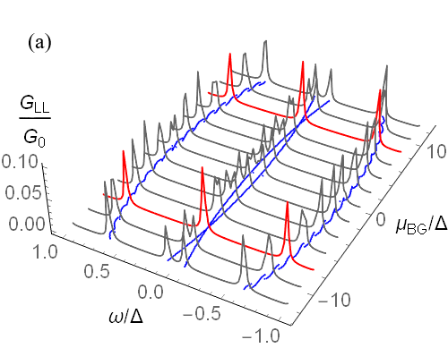
To explicitly show the connection between the tunneling conductace and the subgap spectrum of the quantum device, in the three-dimensional plot of Fig. 2(a) we show the local conductance as a function of frequency in the subgap region (see continuous gray lines), computed for different values of and for the particular values , assuming , , and the experimental ratio . In addition, in the basal plane of this figure we have plotted in continuous blue lines the evolution of the subgap spectrum of (i.e., the ABS levels) as a function of . Due to the particle-hole symmetry of Eq. (11), the subgap spectrum shown in the basal plane of Fig. (2) reflects the symmetry with respect to the line .


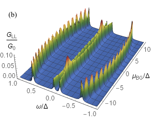
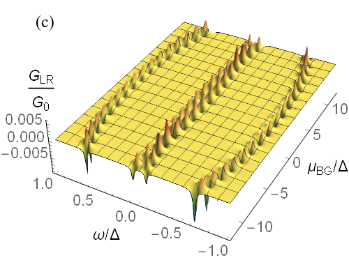
Note that the maxima of the resonances in occur precisely for . Therefore, the bias voltages are suitable experimental quantities allowing to extract the position of the ABS. When the chemical potential is chosen such that one of the ABS levels is tuned through the line (Fermi energy), a QPT is expected to occur in the system (see red continuous lines). In Fig. 2(b) we show a finer mesh computation of where the maxima of the conductance display oscillations related to the presence of nearly degenerate ABS states with even and odd spatial inversion symmetry, due to the inversion symmetry of the Hamiltonian of the system [26]. Finally, in Fig. 2(c) we show a similar calculation for the non-local conductance , which show similar albeit attenuated effects due to the exponential decay of the ABS wavefunctions. Therefore, our results in Fig. 2 show that quantum transport measurements on charge-modulated devices, as the one under study, is a suitable tool to detect the occurrence of QPTs.
The above results are the basis of the spectroscopic transport techniques. Interestingly, we note that additional important information can be extracted from the transport data, in particular, from the derivative of the curve with respect to . To fix ideas, let us focus on the Hamiltonian of the isolated hybrid in Eq. (1). For a generic normalized eigenstate , we have . Applying the Hellmann-Feymann theorem [36] (with the difference that here we are interested in single-particle states, and not on the ground state), we have
| (54) |
where is the total charge operator in the isolated SE-SC-FMI nanowire. Therefore, from the above arguments, we conclude that the experimental quantity allows to obtain the particular average nature (i.e., particle-like or hole-like) of the Bogoliubov-de Gennes eigenstate . While the above derivation has been particularized for the finite and idealized Hamiltonian , note that this is a generic feature of all eigenstates. In the case of the devices discussed here, this information can be useful to detect the particle-hole symmetry point of the device as a function of , and for the particular case of the present discussion, to gain insight into the different nature of the phases before and after a QPT.
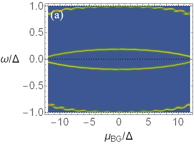
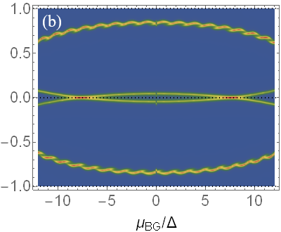
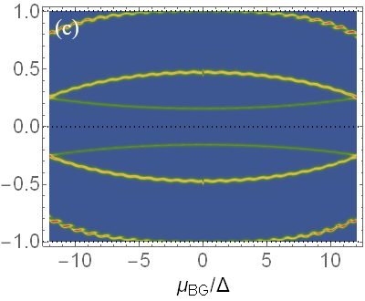
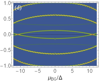
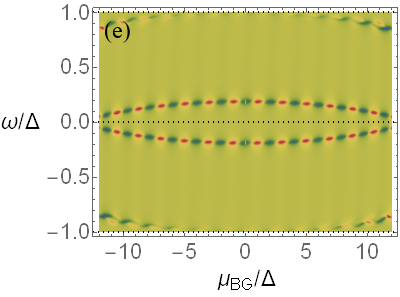
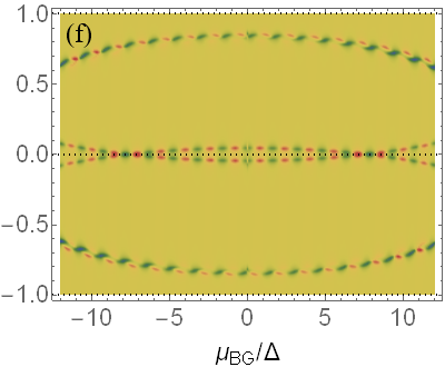
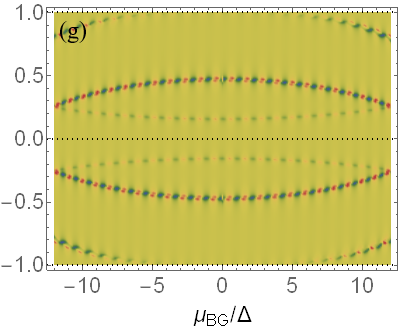
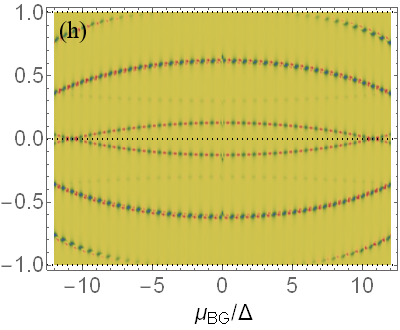
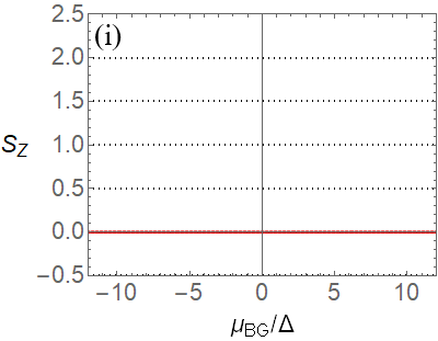
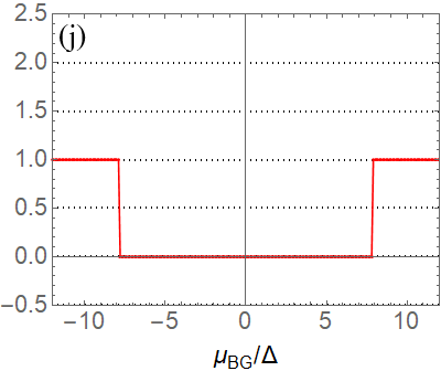
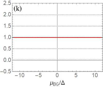
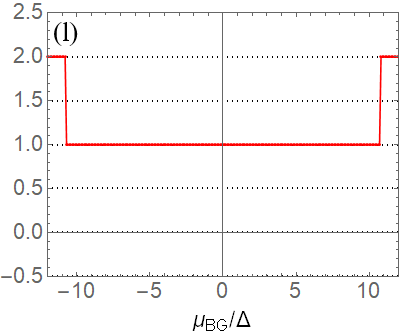
We now study the effect of varying the parameter (effectively representing the length of the FMI layer ) in the behaviour of the device. In Fig. 3 we show colormaps of the local and non-local conductances (first and second rows, respectively) as functions of both the bias voltage (represented by ) and the chemical potential . For each column in Fig. 3 we have used a different value of , starting from and ending in . Beginning from , the curves defined by the evolution of as function of show the presence of 2 pairs of ABS, none of which cross zero, indicating that the device is in a single quantum phase characterized by (see the bottom row in Fig. 3). In addition, the evolution of the derivative indicates that the two ABS in the negative frequency region have the same qualitative behavior, changing from particle-like for to hole-like for , as expected for Bogoliubons formed in a conduction band that is less or more than half-filled, respectively. Note in addition that the point , where , corresponds to the particle-hole symmetric point in the model, as expected. In the region , the other two ABS curves correspond to the particle-hole partners of the lower ABS, which behave in the opposite way.
The presence of only 2 ABS pairs in our calculated spectrum points to a physical situation which is qualitatively similar to that found in Ref. [18], where 1 pair of ABS (and not many) has been found experimentally. Despite the differences, this fact indicates that the parameter estimation made in Sec. II is reasonable.
By increasing the length of the FMI layer to , we see the appearance of two quasidegenerate ABS crossing zero energy at , indicating the occurrence of QPTs at these points, the connection between the occurrence of ABS crossing the Fermi level, and the corresponding value of has been studied in Ref. [37]. While the region is characterized by , the region corresponds to . The new subgap spectrum can be interpreted in terms of the previous one for , in which the two lower (upper) ABS curves have been shifted upwards (downwards) by the effect of a larger Zeeman interaction. Increasing even further to , we see that the region with has disappeared. For the range of values shown, the first ABS curve has completely crossed below zero-energy, saturating at a value of , corresponding to the limits of the energy interval where the ABS are located within the gap. (see Ref. [26]). A second ABS curve moves toward zero, while a third curve emerges from the edge of the gap. For this value of , in both the and regions of the Figure we observe a coexistence of ABS with different curvature and therefore, by virtue of Eq. (54), of different nature (i.e., some are particle-like, other hole-like). We speculate that this coexistence is a model-independent feature of quantum phases with in this type of device. Finally, in the last column in Fig. 3 we show the subgap conductance corresponding to a device with a FMI layer of length . In that case we observe a new QPT corresponding to a second pair of ABS crossing zero energy at . Consequently, a ground state characterized by in the region , and by in the region , emerges, showing the aforementioned coexistence of ABS bands of different nature.
The marked different behaviour of the subgap transport features confirms that the operation regime of the device strongly depends on the geometric parameters. As already mentioned, the relevant parameter controlling the position of the ABS is the dimensionless product [26]. Although experimentally it would be difficult to have precise control over , the Fermi momentum can be in situ controlled via the back gate , providing a more accessible way to explore the quantum phase diagram of the device.
V Summary and conclusions
In this work we have studied the transport properties of one-dimensional heterostructures realizing semiconductor-superconductor-ferromagnetic insulator (SE-SC-FMI) triple interfaces. These devices have been recently fabricated using molecular beam-epitaxy growth techniques, and constitute an interesting example of a novel quantum device with tailored properties arising from the combination of materials. While most studies in these hybrid devices have focused on the potential generation of topological superconductor structures with Majorana fermions, in this work we put forward a different application, i.e., the use of these hybrids to study a highly tunable device displaying controllable quantum phase transitions which can be detected via transport measurements.
We stress that the studied device differs from existing realizations in two fundamental aspects: a) the length of the FMI layer is shorter than the length of the SE-SC heterostructure, thereby introducing an inhomogeneous Zeeman interaction which has important effects on the induced ABS, and b) we consider SE nanowires with no (or very weak) Rashba spin-orbit interaction, a fact that allows to induce spin-polarized ABS and to induce high-spin quantum ground states. Experimentally, the first requirement can be realized using appropriate masks (i.e., shadow-wall technique) in the MBE growth of the FMI layer. In addition, the second requirement could be acomplished by growing SE nanowires using centrosymmetric materials, such as silicon (Si). Finally, a crucial assumption consists in the possibility to modulate the total charge on the device via the presence of a uniform backgate . This is a point which have been experimentally demonstrated in recent experiments with similar devices [17, 18]. Therefore we believe these three requirements are within experimental reach and could be well met in specific realizations.
Using reasonable values for the parameters in our model, our results indicate that by controlling both and/or , the device can be tuned across QPTs in which the fermion parity and the total of the ground state abruptly change. As shown in Figs. 2 and 3, the zero-energy crossings of the subgap ABS as a function of (via ) would be an indication of such QPTs. We stress that using more involved experimental methods (i.e., Coulomb-blockade transport technique), tunable ABS crossing the Fermi energy have been already detected [18].
For completeness, it is worth discussing here the limit , in which the magnetic region becomes very small (much smaller than the Fermi wavelength of the device) in the presence of a very strong Zeeman field , such that the product is kept constant. Under such conditions, the magnetic profile simplifies to a delta function and the setup mimics the physics an atomic Yu-Shiba-Rusinov classical impurity [38, 39, 40], in which the resulting ABS have been proposed as fundamental building blocks to engineer quantum devices with topologically non-trivial ground states [41, 42, 43]. In this case, the ABS with odd spatial symmetry with respect to the center of the magnetic profile decouple, as they have vanishing weight at the magnetic region, and only ABS with even symmetry survive in the subgap region. The theoretical prediction in that case is that a parity- and spin-changing QPT would occur when satisfies the condition , with the denstity of normal conduction states at the Fermi level [38, 39, 40]. From that perspective, our results are a generalization of the impurity case to situations where the magnetic region is extended, and therefore more QPTs are expected to occur (see also Ref. [26]).
Finally, we stress that in our calculations we have neglected many experimentally relevant effects: disorder, multiple conduction channels, finite temperature, electron-electron interaction, etc. While our results will certainly be modified if these effects are taken into account, we expect they will not affect our conclusions qualitatively, in particular the existence of parity- and spin-changing QPTs in this type of devices, and the possibility of their experimental detection. A notable exception is the presence of residual spin-orbit coupling producing a mixing of ABS branches with different spin projections, which would lift the degeneracy whenever two such branches become degenerate. In particular, spin-orbit coupling would generate avoided crossings instead of zero-energy crossings, which would modify the properties of the QPTs discussed in this work. However, we believe that this particular effect would be minimized using centrosymmetric SE materials, such as silicon, instead of InAs.
Acknowledgements.
This work is partially supported by CONICET, Universidad Nacional de La Plata (UNLP) and Universidad Nacional de Cuyo (UNCuyo), Argentina.Appendix A From finite to infinite superconducting chain: Embedding procedure to eliminate finite-size effects
A.1 Local Nambu Green’s function of a semi-infinite chain
In this section, we derive the expressions for and that we need in order to couple the semi-infinite chains to the central region via Eq. (35). For simplicity, we describe here a generic semi-infinite chain whose site labels range from to with the following Hamiltonian
| (55) |
which we can identify with the semi-infinite Hamiltonians in Eqs. (5) and (6). Since the corresponding Green’s function matrix is formally infinite, we define the spatially-projected retarded Green’s function matrix on sites in Nambu space as
| (56) |
where is the (infinite) BdG Hamiltonian matrix corresponding to Eq. (55).
We now introduce a new site , identical to all other sites in Eq. (55), to the left of the chain. It is evident that the system remains the same (i.e., it is a semi-infinite chain). The BdG Hamiltonian of this new site in the basis is
| (57) |
and it couples to the site through the term (see Eq. (37))
| (58) |
where is the Pauli matrix along . Note that we have dropped the spin index in the above expressions as these portions of the nanowire are SU(2) symmetric. Since we are interested in the local Green’s function , we can use Dyson’s equation:
| (59) | ||||
| (60) |
where is the Nambu Green’s corresponding to the isolated site
| (61) |
where . Replacing Eq. (60) into Eq. (59), and noticing that , we find a closed equation for the matrix :
| (62) |
The Eq. (62) defines a coupled system of quadratic equations for the 4 Nambu elements of that can be solved analytically:
| (63) | ||||
| (64) | ||||
| (65) | ||||
| (66) |
where for compactness the frequency argument has been avoided. These expressions can be simplified to
| (67) | ||||
| (68) | ||||
| (69) | ||||
| (70) |
where we have defined , and
| (71) | ||||
| (72) |
In the above expressions, the sign is selected imposing continuity conditions for , and requiring that . Finally, the Green’s functions needed in Eq. (35) are
| (73) |
A.2 Embedding the SE-SC-FMI finite system via the Dyson’s equation
As mentioned in Sec.(III.3), to eliminate finite-size effects we couple the central region in Fig. 1 (containing the SE-SC-FMI hybrid structure already connected to the contacts Eq. (30)) to semi-infinite SE-SC chains given by Eqs. (5) and (6). The term that couples the finite system to the semi-infinite chains is Eq. (7). Therefore the Dyson’s equation that dresses the central part is
| (74) |
This is a formally infinite matrix equation, which can be projected onto the sites corresponding to the central region, and solved quasi-analytically for the site-projections of Eq. (74) that are needed for the transport properties [i.e., Eqs. (50)-(53)]
| (75) | ||||
| (76) |
where in the first line we have omitted the frequency argument for compactness, and where we have used the result , obtained in Eq. (73). We only need 4 projections of the fully dressed Green’s functions to obtain the local and non-local conductance [see Sec.(III.4)]
| (77) | ||||
| (78) | ||||
| (79) | ||||
| (80) |
where we have defined the quantities
| (81) |
These dressed Green’s functions form a linear set of equations that can be solved analytically. Solving first for and from Eqs. (79) and Eq. (80) respectively
| (82) | ||||
| (83) |
and replacing into Eqs. (77) and (78), we reduce the unknowns to two independent Green’s functions
| (84) | ||||
| (85) |
Finally, we find and in Eq. (84) and Eq. (85) in terms of finite matrix Greens functions that can be solved numerically
| (86) | ||||
| (87) |
where we have defined .
Appendix B Conductance
In this Appendix, we present details of the calculation of the local and non-local conductances in Eqs. (50)-(53). For simplicity, in what follows we focus on the derivation of the current flowing through the left contact appearing in Eq. (42), the same procedure can be applied to the right lead. In addition, we omit spin indices to simplify the notation.
Using Dyson’s equation in the Keldysh formalism using Eq. (4) as the perturbation connecting the (infinite) SE-SC-FMI system to the contact leads, the lesser Nambu Green’s functions in Eq. (42) can be expressed as
| (88) | ||||
| (89) |
where the labels and denote time-ordered and anti time-ordered Green’s functions, respectively [30]. Substracting the left handsides, we obtain
| (90) | ||||
| (91) |
where we have used the Keldysh Green’s functions identity [30]. Replacing this result in Eq. (42), and restoring the spin indices and the frequency arguments we obtain
| (92) |
which corresponds to Eq. (43). We recall that the notation denotes the first element of the Nambu Green’s function matrix. We now replace the expressions of the bare Green’s functions and given by Eqs. (46) and Eq. (47) respectively, and obtain
| (93) | ||||
| (94) | ||||
| (95) | ||||
| (96) |
where we have used another Keldysh identity [30]. In order to take the derivatives with respect to the chemical potentials and , the lesser Green’s function in the right handside of Eq. (96) must be expanded in term of local lesser Green’s function at the leads and , for this purpose we use the Dyson-Keldysh equation [29, 30]
| (97) |
where , and where is the BdG-Nambu Hamiltonian corresponding to Hamiltonian Eq. (4). Deriving the first element of the Nambu Green’s function matrix in Eq. (96) allows to obtain
| (98) | ||||
| (99) |
Finally, replacing Eq. (98) and Eq. (99) into Eq. (96), the local and non-local conductance depend explicitly on the derivatives of the Fermi distribution
| (100) | ||||
| (101) |
References
- Hübler et al. [2012] F. Hübler, M. J. Wolf, T. Scherer, D. Wang, D. Beckmann, and H. v. Löhneysen, Phys. Rev. Lett. 109, 087004 (2012).
- Bergeret et al. [2005] F. S. Bergeret, A. F. Volkov, and K. B. Efetov, Rev. Mod. Phys. 77, 1321 (2005).
- Eschrig [2018] M. Eschrig, Phil. Trans. R. Soc. A 376, 20150149 (2018).
- Bergeret et al. [2018] F. S. Bergeret, M. Silaev, P. Virtanen, and T. T. Heikkilä, Rev. Mod. Phys. 90, 041001 (2018).
- Heikkilä et al. [2019] T. T. Heikkilä, M. Silaev, P. Virtanen, and F. S. Bergeret, Prog. Surf. Sci. 94, 100540 (2019).
- Diesch et al. [2018] S. Diesch, P. Machon, M. Wolz, C. Sürgers, D. Beckmann, W. Belzig, and E. Scheer, Nat. Commun. 9, 5248 (2018).
- Minutillo et al. [2021] M. Minutillo, R. Capecelatro, and P. Lucignano, Phys. Rev. B 104, 184504 (2021).
- Mourik et al. [2012] V. Mourik, K. Zuo, S. M. Frolov, S. Plissard, E. A. Bakkers, and L. Kouwenhoven, Science 336, 1003 (2012).
- Das et al. [2012] A. Das, Y. Ronen, Y. Most, Y. Oreg, M. Heiblum, and H. Shtrikman, Nat. Phys. 8, 887 (2012).
- Deng et al. [2012] M. T. Deng, C. L. Yu, G. Y. Huang, M. Larsson, P. Caroff, and H. Q. Xu, Nano Lett. 12, 6414 (2012).
- Rokhinson et al. [2012] L. P. Rokhinson, X. Liu, and J. K. Furdyna, Nat. Phys. 8, 795 (2012).
- Churchill et al. [2013] H. O. H. Churchill, V. Fatemi, K. Grove-Rasmussen, M. T. Deng, P. Caroff, H. Q. Xu, and C. M. Marcus, Phys. Rev. B 87, 241401 (2013).
- Finck et al. [2013] A. D. K. Finck, D. J. Van Harlingen, P. K. Mohseni, K. Jung, and X. Li, Phys. Rev. Lett. 110, 126406 (2013).
- Lutchyn et al. [2010] R. M. Lutchyn, J. D. Sau, and S. Das Sarma, Phys. Rev. Lett. 105, 077001 (2010).
- Oreg et al. [2010] Y. Oreg, G. Refael, and F. von Oppen, Phys. Rev. Lett. 105, 177002 (2010).
- Liu et al. [2020] Y. Liu, S. Vaitiekėnas, S. Martí-Sánchez, C. Koch, S. Hart, Z. Cui, T. Kanne, S. A. Khan, R. Tanta, S. Upadhyay, M. E. Cachaza, C. M. Marcus, J. Arbiol, K. A. Moler, and P. Krogstrup, Nano Lett. 20, 456 (2020).
- Vaitiekėnas et al. [2021] S. Vaitiekėnas, Y. Liu, P. Krogstrup, and C. M. Marcus, Nat. Phys. 17, 43 (2021).
- Vaitiekėnas et al. [2022] S. Vaitiekėnas, R. S. Souto, Y. Liu, P. Krogstrup, K. Flensberg, M. Leijnse, and C. M. Marcus, Phys. Rev. B 105, L041304 (2022).
- Woods et al. [2021] B. D. Woods, S. Das Sarma, and T. D. Stanescu, Phys. Rev. Appl. 16, 054053 (2021).
- Maiani et al. [2021] A. Maiani, R. Seoane Souto, M. Leijnse, and K. Flensberg, Phys. Rev. B 103, 104508 (2021).
- Liu et al. [2021] C.-X. Liu, S. Schuwalow, Y. Liu, K. Vilkelis, A. L. R. Manesco, P. Krogstrup, and M. Wimmer, Phys. Rev. B 104, 014516 (2021).
- Langbehn et al. [2021] J. Langbehn, S. Acero González, P. W. Brouwer, and F. von Oppen, Phys. Rev. B 103, 165301 (2021).
- Khindanov et al. [2021] A. Khindanov, J. Alicea, P. Lee, W. S. Cole, and A. E. Antipov, Phys. Rev. B 103, 134506 (2021).
- Escribano et al. [2022] S. D. Escribano, A. Maiani, M. Leijnse, K. Flensberg, Y. Oreg, A. Levy Yeyati, E. Prada, and R. Seoane Souto, npj Quantum Mater. 7, 81 (2022).
- Singh and Muralidharan [2023] R. Singh and B. Muralidharan, Commun. Phys. 6, 36 (2023).
- Feijoo et al. [2023] J. Feijoo, A. Iucci, and A. M. Lobos, Phys. Rev. B 107, 214505 (2023).
- Balatsky et al. [2006] A. V. Balatsky, I. Vekhter, and J.-X. Zhu, Rev. Mod. Phys. 78, 373 (2006).
- Note [1] S. Vaitiekėnas, private comunication.
- Cuevas et al. [1996] J. C. Cuevas, A. Martín-Rodero, and A. Levy Yeyati, Phys. Rev. B 54, 7366 (1996).
- Haug and Jauho [2007] H. Haug and A. Jauho, Quantum Kinetics in Transport and Optics of Semiconductors, Springer Series in Solid-State Sciences (Springer Berlin Heidelberg, 2007).
- Datta [1995] S. Datta, Electronic Transport in Mesoscopic Systems (Cambridge University Press, Cambridge, 1995).
- Meir and Wingreen [1992] Y. Meir and N. S. Wingreen, Phys. Rev. Lett. 68, 2512 (1992).
- Mahan [1981] G. D. Mahan, Many particle physics (Plenum, New York, 1981).
- Tinkham [1996] M. Tinkham, Introduction to Superconductivity, 2nd Edition (McGraw-Hill, Inc., New York, 1996).
- Sakurai [1970] A. Sakurai, Prog. Theor. Phys. 44, 1472 (1970).
- Feynman [1939] R. P. Feynman, Phys. Rev. 56, 340 (1939).
- Rouco et al. [2019] M. Rouco, I. V. Tokatly, and F. S. Bergeret, Phys. Rev. B 99, 094514 (2019).
- Luh [1965] Y. Luh, Acta Phys. Sin. 21, 75 (1965).
- Shiba [1968] H. Shiba, Prog. Theor. Phys. 40, 435 (1968).
- Rusinov [1968] A. I. Rusinov, Zh. Eksp. Teor. Fiz. Pisma. Red. 9, 146 (1968), [JETP Lett. 9, 85 (1969)].
- Nadj-Perge et al. [2013] S. Nadj-Perge, I. K. Drozdov, B. A. Bernevig, and A. Yazdani, Phys. Rev. B 88, 020407 (2013).
- Klinovaja et al. [2013] J. Klinovaja, P. Stano, A. Yazdani, and D. Loss, Phys. Rev. Lett. 111, 186805 (2013).
- Li et al. [2014] J. Li, H. Chen, I. K. Drozdov, A. Yazdani, B. A. Bernevig, and A. H. MacDonald, Phys. Rev. B 90, 235433 (2014).