Ultrabroadband tunable difference frequency generation in standardized thin-film lithium niobate platform
††journal: opticajournal††articletype: Research ArticleThin-film lithium niobate (TFLN) on insulator is a promising platform for nonlinear photonic integrated circuits (PICs) due to its strong light confinement, high second-order nonlinearity, and flexible quasi-phase matching for three-wave mixing processes via periodic poling. Among the three-wave mixing processes of interest, difference frequency generation (DFG) can produce long wave infrared (IR) light from readily available near IR inputs. While broadband DFG is well studied for mid-IR frequencies, achieving broadband idler generation within the telecom window (near C-band) and the short-wave infrared (near 2 micron) is more challenging due to stringent dispersion profile requirements, especially when using standardized TFLN thicknesses. In this paper, we investigate various standard waveguide designs to pinpoint favorable conditions for broadband DFG operation covering several telecom bands. Our simulations identify viable designs with a possible 3-dB conversion efficiency bandwidth (CE-BW) of 300 nm and our measurements show idler generation from 1418 nm to 1740 nm, limited by our available sources, experimentally confirming our design approach. Furthermore, temperature tuning allows further shift of the idler towards the mid-IR, up to 1819 nm. We also achieve a stretched wavelength range of idler generation by leveraging the longitudinal variation of the waveguide in addition to poling. Finally, our numerical simulations show the possibility of extending the CE-BW up to 780 nm while focusing on waveguide cross-sections that are available for fabrication within a foundry. Our work provides a methodology that bridges the deviations between fabricated and designed cross-sections, paving a way for standardized broadband DFG building blocks.
1 Introduction
Many photonic integrated circuit (PIC) platforms, such as silicon (Si) or silicon nitride (SiN), lack intrinsic second-order susceptibility (), relying instead on third-order susceptibility () for nonlinear frequency conversion. However, enables nonlinear responses even at moderate input powers. Lithium niobate (LN), which exhibits high ( -25.2 pm/V where = 2 [1]) emerges as a promising PIC platform. Thin-film LN (TFLN), available as a single crystal LN layer over the entire handling silicon-on-insulator wafer[2, 3], combined with advances in etching techniques[4, 5], allows for low-loss waveguides with strong light confinement. Furthermore, LN’s ferroelectric nature enables microscale crystal orientation control by applying high-voltage ms-pulses from periodic metal electrodes, whose periodicity, precisely inscribed by lithography, becomes a design parameter[6]. This technique, i.e. periodic poling, offers versatile means to achieve quasi phase-matching (QPM) conditions making TFLN particularly favorable for nonlinear frequency generation.
This work focuses on difference-frequency generation (DFG) using periodically-poled TFLN waveguides. DFG can carry out optical parametric oscillation (OPO) and amplification (OPA), facilitating optical processing and coherent amplification [7, 8]. Moreover, DFG can support broadband generation of frequencies that are challenging to reach using conventional lasing materials. It was demonstrated for mid-IR frequencies covering idler wavelengths from 2.6 m to 4 m in TFLN on sapphire substrates at high temperatures (>175°C) [9] and for signal wavelengths around 2 m (with a bandwidth 600 nm) [10]. Near the C-band transmission window (around 1550 nm), broadband idler generation has proved to be challenging due to more stringent restrictions in terms of achievable dispersion profiles. Nevertheless, DFG idler bandwidths up to 100 nm were demonstrated experimentally [11, 12, 13, 14]. Furthermore, spontaneous idler generation without requiring the signal input, i.e. spontaneous parametric down conversion (SPDC), is also investigated for broadband response with potential applications in quantum signal processing [15, 16, 17].
In this work, we design periodically poled waveguides for broadband DFG at telecom wavelengths, and specifically identify favourable cross-sections on a standardized TFLN platform, with a vision to incorporate nonlinear building blocks in the TFLN process design kit (PDK). We theoretically calculate the QPM DFG poling period, conversion efficiency (CE), and bandwidth. We experimentally validate one of our designs by measuring the broadband idler generation over a 300 nm wide wavelength range covering several telecom bands and demonstrate enhanced bandwidth towards mid-IR via temperature tuning. We also investigate the effect of longitudinal waveguide fluctuations by comparing the nonlinear response of two different waveguides and leverage this inhomogeneity for broadband operation.
2 Dispersion Engineering and Design
Our analysis focuses on QPM DFG between fundamental TE modes of pump, signal and idler on a waveguide assuming perfect square poling. We perform numerical mode simulations (in Ansys Lumerical) and calculate poling period (), and CE at a selected poling period using Eq. 1 and Eq. 2 [18, 19]:
| (1) |
| (2) |
where , and are effective index, wavelength and power of signal/pump/idler, respectively, and is the periodically poled waveguide length. In the following analysis (throughout Sec. 2), we present the simulation results for = 5 mm.
| (3) |
| (4) |
where is the signal/pump/idler electric field.
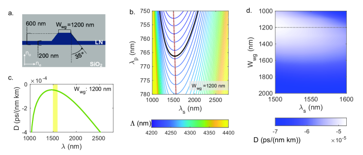
We first engineer the DFG response via (Fig. 1b) calculated for different and with the waveguide cross-section given in Fig. 1a, compatible to the TFLN PIC foundry of CSEM[20] . For each , two distant phase matched regions merge as approaches the second-harmonic (SH) wavelength (), which also corresponds to near-degenerate DFG (). This wavelength relation is labelled in Fig. 1b as the red dashed line and referred as SH-line hereafter. We observe that remains relatively constant near the SH-line and as a result, this region becomes favorable for broadband operation.
In this paper, we focus on optimizing the broadband response while sweeping at a fixed . For the -sweep, conversion efficiency 3 dB bandwidth (CE-BW) is conventionally associated with the group velocity mismatch (GVM) between signal and idler. Yet, near the SH-line, GVM approaches zero as . As a result, higher order dispersion terms like the group velocity dispersion (D) starts to influence the bandwidth. For illustration, we plot in Fig. 1c, D for the cross-section given in Fig. 1a where the signal wavelength range of interest is highlighted.
With the motivation of maximizing CE-BW, we extend the design space, considering varying waveguide widths () while keeping the etch angle and the TFLN thickness constant, hence maintaining compatibility with the standardized platform. We numerically calculate D for each ranging from 1000 nm to 2000 nm and for the same wavelength range highlighted in Fig. 1c.
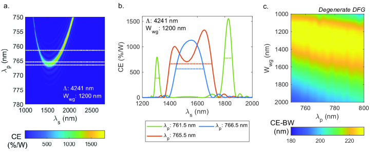
Our simulations indicate that minimum magnitude of D () occurs between = 1100 nm and = 1400 nm (Fig. 1d). In literature, waveguides with near-zero D are associated with broad bandwidth and favored for different nonlinear processes like SPDC and four-wave mixing (FWM) [21, 22]. The presented cross-section (Fig. 1a) with = 1200 nm lies in this favorable region. Therefore, we continue the analysis in the same cross-section by calculating CE (Eq. 2). The CE at a selected of 4241 nm, which is labelled in black on Fig. 1b and is phase-matched for degenerate DFG () at 766.5 nm, is shown in Fig. 2a. The CE for a few selected pump wavelengths is plotted in Fig. 2b. We see that for = 766.5 nm (blue line) we obtain one broadband phase-matched peak. Then, as is slightly detuned, the two phase-matched regions start separating. For 765.5nm (orange line), we obtain the broadest CE-BW estimated at 307 nm and idler generation from 1357 nm to 1758 nm. We also observe the complete separation of the phase matched regions for shorter . For example, CE(@ = 761.5 nm) has two different phase-matched regions present at around 1307 nm and 1827 nm with CE-BW of 29 nm and 59 nm, respectively (green line). Overall, we show tunable CE-BW from 29 nm to 307 nm via adjusting .
We also extend the CE calculations to different cladded cross-sections at the optimized to operate at degenerate DFG regime (). In Fig. 2c, we plot CE-BW for different ranging from 1000 nm to 2000 nm for ranging from 750 nm to 800 nm. D for all corresponding to the described operating point is already presented in Fig. 1c. In this design space, we indeed see that the maximum CE-BW occurs on minimum , verifying the proposed link between CE-BW and D in near degenerate DFG regime.
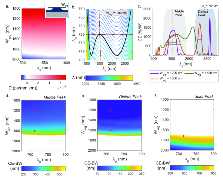
Next, we repeat the analysis for an uncladded configuration, which gives an extra degree of freedom, in addition to the waveguide dimensions, in terms of dispersion engineering. In Fig. 3a, we plot D at different and . We observe that most of the investigated waveguides are in the anomalous dispersion regime in contrast to previous configuration. Due to this difference, we start from one (namely 1200 nm which has strong anomalous dispersion) and calculate at different and (Fig. 3b). We observe that, when the is phase-matched to satisfy degenerate DFG ( = ), it is also phase-matched for a distant signal/idler pair at the same . As an illustration, we carry the following analysis for = 765 nm and with the corresponding highlighted in black in Fig. 3b. The calculated CE is shown in purple in Fig. 3c. It is characterized by three phase-matched regions located at = 1089 nm, = 1530 nm and = 2568 nm) where the middle one fulfills the degenerate DFG condition. The peaks of interest referred as "middle peak" and "distant peak" are labelled in Fig. 3c.
The influence of dispersion on this three phase matched regions is carried by extending the CE calculations for different and is also illustrated in Fig. 3c. As increases, D can remain anomalous but becomes smaller (see Fig. 3a). For example, for = 1600 nm (orange line), we observe that the CE-BW of the "middle peak" increases while the "distant peak" shifts towards the "middle peak". When is further increased, D approaches to near-zero dispersion and the phase-matched bands starts to overlap. Particularly, at = 1720 nm (green line), we obtain a continuous range of idler generation from 1160 nm to 2253 nm and a CE-BW of 782 nm.
We further extend the design space and calculate the CE-BW for all and when the is quasi phase-matched for degenerate DFG. We calculate the CE-BW of the "middle" or "distant" peaks if the respective peak’s -3dB intensity level does not cross the other peak. We label the data points that are plotted in Fig. 3c with red markers. In the "middle peak" ("distant peak"), CE-BW can be tuned from 200 nm (40 nm) to 600 nm (220 nm) by precisely selecting as shown in Fig. 3d (Fig. 3e). CE-BW of both "middle peak" and "distant peak" increases with increasing for all . We additionally calculate CE-BW of the "joint peak" when the CE-BW cannot be individually determined for neither "middle peak" nor "distant peak". We observe the broadest bandwidth on the "joint peak" right after the peaks merger, which can exceed 780 nm. Overall, within this entire design space, it is possible to have a tunable CE-BW covering the telecom bands from 200 nm to 780 nm near the degenerate DFG regime by controlling .
To summarize, in this section, we have presented a detailed analysis of optimizing , and the waveguide cross-section to either achieve highest CE-BW or to precisely tune CE-BW. We obtain maximum CE-BW of 300 nm in the cladded configuration and 780 nm in the uncladded configuration. To our knowledge, this analysis provides one of the widest bandwidths foreseen for any TFLN waveguide relying on DFG [14, 21, 17, 15, 23, 10, 9].
3 Optical Characterization of Fabricated Waveguides
We experimentally verify our analysis on one of the favorable broadband cladded cross-sections with = 1200 nm (Fig. 1a). Several waveguides with these nominal dimensions and 4.8 mm PPLN length were fabricated at CSEM in a die size of 5x5 mm2 on different wafers and poled by applying high-voltage millisecond pulses to the periodically patterned electrodes. To take into account possible wafer to wafer fluctuations, we patterned electrodes with different (namely 4100 nm, 4200 nm and 4300 nm).
The setup used for optical characterization is shown in Fig. 4a. The chip is placed on a temperature controlled stage that is constructed from a PID controller and a Peltier element. Different tunable telecom lasers (Yenista Tunics T100) and an NIR laser (Newfocus TLB-6700) are used to sweep and , respectively. For sweeps, we aim to observe both the generated idler peak and its sidelobes for a selected . In this case, we amplify a fixed telecom signal with an EDFA and reduce the noise floor by placing a band-pass filter (BPF) after the amplifier. We control the polarization of both inputs and combine them after isolators with a wavelength-division multiplexer (WDM). We use lensed fibers (cone angle = 90∘ 5∘) for coupling in and out from the chip. We record the outcoupled pump, signal and idler spectra in an optical spectrum analyser (OSA Yokogawa AQ6370). For sweeps at a fixed , we optimize the setup for sweeping a wide wavelength range from 1250 nm to 1660 nm while minimizing losses. Consequently, we remove the EDFA, band-pass filter, isolator and NIR polarization controller from the signal path. For outcoupling the broadband light from the chip, we use an objective (NA = 0.35) followed by a reflective collimator which delivers light to the OSA (Yokogawa AQ6375).
Prior to DFG characterization, we also measure the SH-response in the same setup by coupling only the telecom laser into the chip from a lensed fiber. We outcouple the light with the objective and separate telecom-input and generated-SH with a dichroic mirror (DMSP). With this technique, we simultaneously detect telecom-input and generated SH from individual powermeters (PM).
3.1 Effective Poling Period on Fabricated Waveguide
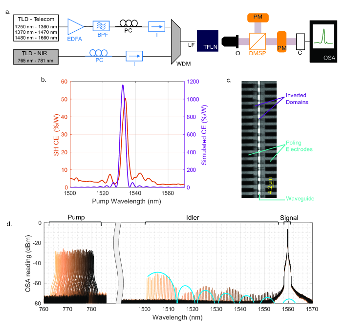
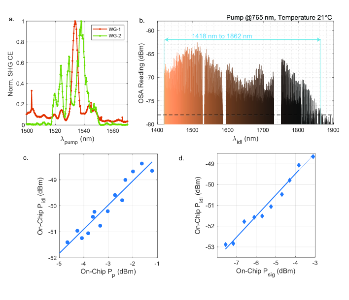
We perform SH measurements and identify a waveguide (WG-1) with the SH-peak at 1533 nm corresponding to = 4241 nm for the simulated design cross-section. In Fig. 4b, we plot the measured SH CE (calculated as ) for WG-1 and overlay with the simulations for = 4241 nm as it differs from the actual poling period because of fabrication tolerances [24]. We refer to the = 4241 nm as the effective poling period of WG-1 as it facilitates the measured response at the targeted design .
We report an acceptable agreement in SH-peak position between simulations (1532.2 nm) and measurements (1533.8 nm). Yet the measured peak intensity is noticeably lower, which we mainly associate with the imperfections on the poling quality. The quality of periodic poling is inspected using two-photon microscopy (TPM). In the TPM image (Fig. 4c), the inverted domains appear darker compared to the unpoled regions and thus indicate underpoling, which can result in a reduced CE. We also recognize the potential role of height fluctuations along the waveguide in the reduced CE [25, 26] (further discussed in Sec. 3.2&4).
After SHG measurements, we characterize DFG in a pump sweep for =1560 nm and ranging from 765 nm to 781 nm. OSA traces are shown in Fig. 4d. We obtain a decent agreement between simulations (full line) and measurements especially on the main peak. We associate the discrepancies on the sidelobes with the imperfections on poling quality and the inhomogeneities in waveguide dimensions. Additionally, we observe prominent wavelength dependent oscillations on the pump and the idler due to the presence of the higher order modes (further elaborated in Sec. 4). Still, with these two sets of independent measurements (SH characterization and DFG pump sweep), we confirm = 4241 nm as the effective poling period of WG-1.
3.2 Broadband DFG and Further Tuning Mechanisms
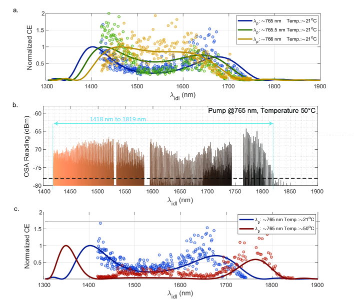
To verify the simulated broadband response of WG-1, we sweep at three (namely 765 nm, 765.5 nm and 766 nm) and record the DFG response on the OSA using the setup illustrated in Fig. 5a. We obtain the total signal and idler powers by integrating the spectral components throughout the measured spectra and calculate the on-chip power by taking wavelength dependent coupling losses into account. To extract coupling losses, we make a fine wavelength sweep and mitigate any oscillations originating from higher order modes by averaging (further discussed in Sec. 4). With this technique, we obtain experimental CE (calculated as ) with respect to (analogously to ). We then fit the intensity of simulated-CE (where and the effective poling period (from Sec. 3.1) are simulation parameters) into the measured data. Both simulated and measured CE are normalized to the maximum value of simulated CE. In Fig. 5a, for each , we plot measured (data points) and simulated (solid lines) normalized CE as a function of .
The measurements are in accordance with the simulations, showing idler generation from 1418 nm to 1740 nm, limited by our available sources. We also observe the separation of the phased-matched regions as the pump is tuned from 766 nm to 765 nm. Furthermore, we perform another measurement at 50°C whose superimposed OSA spectra is shown in Fig. 5b. In this case, idler generation up to = 1819 nm is measured. We also plot the normalized CE as a function of at different temperatures (namely 21°C and 50°C) as shown in Fig. 5c. In our analysis, this temperature range is equivalent to a 3 nm period shift, hence corresponding to effective poling period of 4244 nm. We demonstrate that idler generation shifts towards mid-IR with increasing temperature.
We then investigate the impact of longitudinal waveguide fluctuations on idler generation. For this purpose, we characterize another waveguide (WG-2) with the same nominal design cross section as WG-1 but with a different SH response as shown in Fig. 6a. The SH spectrum of WG-2 has three distinct peaks indicating the presence of fluctuations in the waveguide cross section along the propagation direction due to TFLN thickness variations on the wafer and etching process uncertainties. We estimate the fluctuation in the total TFLN height to be 2 nm (approximately twice that of WG-1) and the fluctuation of the slab thickness to be around 10% (35% larger than WG1), based on TFLN substrate’s datasheet and ellipsometer measurements performed by CSEM. We calculate the poling period within the presence of mentioned fluctuations along the waveguide. These calculations indicate a shift of tens of nanometres in between the two ends of the waveguide. Wu et al. (2022) demonstrate that a small perturbation like chirping (with a range at around 50 nm) can significantly increase the SHG bandwidth [27]. Here, we experimentally show the broadened DFG response due to longitudinal waveguide fluctuations for a comparable perturbation on . In WG-2, we observe the DFG idler from 1418 nm to 1862 nm, when injecting from 1660 nm to 1294 nm at a fixed temperature (21°C) and (765 nm) (Fig. 6b). This indicates that idler generation is possible from 1294 nm to 1862 nm.
In addition to our main focus, i.e. broadband process, we measured the CE and its dependence on input power in WG-2. This value could be improved in future work with the optimization of the poling quality, as previously stated. To accurately estimate the on-chip power from OSA traces, we scale them with powermeter readings (from Thorlabs S120C and S148C) to account for any calibration loss between the collimator and the OSA input. With this technique, we obtain CE between 4-7 %/W at = 1550 nm and = 765 nm. Finally, we sweep the on-chip pump (signal) power and record on-chip idler (idler) power as shown in Fig. 5c(d). We verify the expected linear dependence of the idler with respect pump and signal inputs.
4 Discussion and Conclusion
| Focus | (nm) | Meas. (nm) | Sim. (nm) | Length (mm) | |
| this work | DFG | 765 | WG1: 1418-1819(2) WG2: 1418-1862(2) | 1160-2250 | 4.8-5 |
| [14] | C-O WC | 1550 | 1290-1360 and 1500-1600(2) | 1250-1650 | 5 |
| [21] | SPDC | 770 | 1200-1600(1) | 1200-2000 | 5 |
| [17] | SPDC | 735 | 1350-1600 | 1350-1600 | 6 |
| [15] | SPDC | 810 | 1500-1620(1) | 1400-1800 | 5.7 |
| [11] | SHG/DFG | 735 | 1524-1581 | n.a. | 6 |
| [23] | OPA | 1550 | 1495-1609 | 1475-1620 | 20 |
| [10] | OPA | 1045 | 1600-2400 (3) | 1600-2800 | 6 |
| [9] | DFG | 1064 | 2800–3800 | 2800–3800 | 5 |
| : Pump Wavelength, Meas. : Wavelength range of experimentally generated idler, Sim. : Wavelength range of generated idler in simulations, Length: Length of periodically poled waveguide (z) C-O WC: C-Band to O-Band Wavelength Conversion, SPDC : Spontaneous Parametric Down Conversion, OPA: Optical Parametric Amplification, (1) limited with photodetection range, (2) limited by available laser sources, (3) limited by OSA detection range, | |||||
In this work, we focus on realization of broadband DFG frequency converters based on CSEM’s TFLN foundry stacks. We deem this as an essential step in view of implementing nonlinear PDK building blocks for large scale TFLN PICs.
We successively optimize , and in different dispersion regimes, namely normal, near-zero and anomalous. For broadband operation, we show that the broadest bandwidth occurs on near-zero dispersion, and we achieve a 3-dB DFG CE bandwidth of 300 nm in cladded configuration and 780 nm in the uncladded configuration through dispersion engineering.
We overlay the results of simulations with measurements by extracting the effective poling period from the SH-peak and obtain a decent agreement with measurements. As the electrode periodicity is defined lithographically and has negligible fabrication error, we associate the discrepancy between this periodicity and the effective poling period with the fabrication deviations from the designed waveguide cross-section [24, 25, 26] and the use of material data from literature [28]. These deviations could modify the phase-matched poling period and consequently, shift the optical response. In our methodology, these are considered as perturbations on the design and accounted for in DFG measurements by using the effective poling period. We emphasize on the consistency of the effective poling period ( = 4241 nm on WG1) in all SHG and DFG measurements with pump and signal sweeps. With this approach, we provide a method to bridge the gap between the targeted design and the characterized waveguide cross-section.
In the measurements, we observe strong wavelength-dependent oscillations, which we associate with the presence of higher-order modes at the pump and signal wavelengths. These modes can originate from the input coupling scheme, as the fiberized WDM and lensed fiber are multi-mode for the pump. These could also couple into the chip since the investigated waveguides do not have any dedicated tapers. For these waveguides, we numerically calculate a total of 4 optical modes at 1550 nm and 11 optical modes at 765 nm in simulations. As a result, it is probable that a portion of light will couple in a different mode from the targeted fundamental TE mode and will not contribute to DFG. Such fluctuations in CE have been studied in literature for different platforms, like SiN, and other photon mixing processes like FWM [29]. They can be minimized by implementing dedicated taper designs for signal and pump. Despite these oscillations, there is a clear agreement between our measurements and simulations.
We also recognize that our measured CE is noticeably lower compared to simulated values. We primarily attribute this with the poling quality. TPM images of the investigated waveguides suggest underpoling (as discussed in Sec. 3.1). Since we perform poling after waveguide patterning, the poled domains start to form on the slab and primarily grow laterally along the slab[30]. As a result, part of the waveguide ridge could remain underpoled even if there is complete inversion on the slab. According to our simulations, when 50% of the total waveguide height is inverted, the peak conversion efficiency is reduced by a factor of 3.8. In our case, the slab is thinner, potentially leading to an even more significant reduction in peak CE. Additionally, the presence of longitudinal variations on waveguide cross-section can limit peak CE, especially on WG-2. In the case of broadband designs, we show that the longitudinal waveguide fluctuations are equivalent to chirping of the poling period. Regardless, we perform the broadband measurements without requiring to any additional optical amplifier in the beam path.
We experimentally obtain DFG idler from 1418 nm to 1740 nm and further broaden the range of idler generation via temperature tuning (up to = 1819 nm) and by leveraging the longitudinal waveguide fluctuations (up to = 1862 nm), thereby extending the operation towards IR. We focus our study on both cladded and uncladded waveguides, with the former being experimentally verified. While we show that uncladded waveguides can offer additional benefit in view of flexible and large bandwidth designs, such approach could require additional optimization in terms of fabrication and poling after waveguide patterning due to increased surface currents affecting the poled domain formation [31, 32].
Compared to prior work on periodically-poled TFLN (Table. 1), our study demonstrates DFG bandwidth improvement both in terms of designs and experiments. We present a core building block of nonlinear optics capable of generating signal and idler wavelengths across the entire telecommunication bands. We acknowledge its potential functionality in a multitude of applications including multichannel wavelength-division multiplexing, broadband comb generation and cascaded supercontinuum generation, all while leveraging its availability in a wafer-scale industrial platform.
Acknowledgments This work is supported by the Swiss National Science Foundation (SNSF) Bridge Discovery project (40B2-0) 203480, ENABLE. The authors acknowledge CSEM cleanroom staff for manufacturing the TFLN chips. We also thank F. Ayhan for valuable help on TFLN poling and N. Balakleyskiy for fruitful discussions on design.
Disclosures The authors declare that there are no conflicts of interest related to this article.
References
- [1] J.-m. Liu, Photonic Devices (Cambridge University Press, 2005).
- [2] K. Nassau, H. J. Levinstein, and G. M. Loiacono, “Ferroelectric lithium niobate. 2. Preparation of single domain crystals,” \JournalTitleJournal of Physics and Chemistry of Solids 27, 989–996 (1966).
- [3] K. Nassau, H. J. Levinstein, and G. M. Loiacono, “Ferroelectric lithium niobate. 1. Growth, domain structure, dislocations and etching,” \JournalTitleJournal of Physics and Chemistry of Solids 27, 983–988 (1966).
- [4] C. Wang, X. Xiong, N. Andrade, et al., “Second harmonic generation in nano-structured thin-film lithium niobate waveguides,” \JournalTitleOptics Express, Vol. 25, Issue 6, pp. 6963-6973 25, 6963–6973 (2017).
- [5] R. Wu, M. Wang, J. Xu, et al., “Long Low-Loss-Litium Niobate on Insulator Waveguides with Sub-Nanometer Surface Roughness,” \JournalTitleNanomaterials 2018, Vol. 8, Page 910 8, 910 (2018).
- [6] D. Zhu, L. Shao, M. Yu, et al., “Integrated photonics on thin-film lithium niobate,” \JournalTitleAdvances in Optics and Photonics, Vol. 13, Issue 2, pp. 242-352 13, 242–352 (2021).
- [7] G. Cerullo and S. De Silvestri, “Ultrafast optical parametric amplifiers,” \JournalTitleReview of Scientific Instruments 74, 1–18 (2003).
- [8] J.-y. Zhang, Optical Parametric Generation and Amplification (Routledge, 2019).
- [9] J. Mishra, M. Jankowski, A. Hwang, et al., “Ultra-broadband mid-infrared generation in dispersion-engineered thin-film lithium niobate,” \JournalTitleOptics Express, Vol. 30, Issue 18, pp. 32752-32760 30, 32752–32760 (2022).
- [10] L. Ledezma, R. Sekine, Q. Guo, et al., “Intense optical parametric amplification in dispersion-engineered nanophotonic lithium niobate waveguides,” \JournalTitleOptica, Vol. 9, Issue 3, pp. 303-308 9, 303–308 (2022).
- [11] Y. Niu, C. Lin, X. Liu, et al., “Optimizing the efficiency of a periodically poled LNOI waveguide using in situ monitoring of the ferroelectric domains,” \JournalTitleApplied Physics Letters 116, 101104 (2020).
- [12] J.-Y. Chen, Y.-P. Huang, and Y. M. Sua, “Ultra-wideband and high-gain parametric amplification in telecom wavelengths with an optimally mode-matched PPLN waveguide,” \JournalTitleOptics Letters, Vol. 43, Issue 12, pp. 2965-2968 43, 2965–2968 (2018).
- [13] H. Sasaki, H. Murai, T. Kishimoto, et al., “Highly efficient phase-sensitive parametric gain in periodically poled LiNbO<sub>3</sub> ridge waveguide,” \JournalTitleOptics Letters, Vol. 41, Issue 9, pp. 1905-1908 41, 1905–1908 (2016).
- [14] J. Wei, C. Cheng, Y. Wu, et al., “Efficient and Broadband All-Optical Wavelength Conversion between C and O Bands in Nanophotonic Lithium Niobate Waveguides,” \JournalTitleJournal of Lightwave Technology (2024).
- [15] X.-X. Fang, L. Wang, and H. Lu, “Efficient generation of broadband photon pairs in shallow-etched lithium niobate nanowaveguides,” \JournalTitleOptics Express, Vol. 32, Issue 13, pp. 22945-22954 32, 22945–22954 (2024).
- [16] U. A. Javid, J. Ling, J. Staffa, et al., “Ultrabroadband Entangled Photons on a Nanophotonic Chip,” \JournalTitlePhysical Review Letters 127, 183601 (2021).
- [17] G. T. Xue, Y. F. Niu, X. Liu, et al., “Ultrabright Multiplexed Energy-Time-Entangled Photon Generation from Lithium Niobate on Insulator Chip,” \JournalTitlePhysical Review Applied 15, 064059 (2021).
- [18] T. Suhara and M. Fujimura, Waveguide Nonlinear-Optic Devices, vol. 11 of Springer Series in Photonics (Springer Berlin Heidelberg, 2003).
- [19] R. L. Sutherland, Handbook of Nonlinear Optics (CRC Press, 2003).
- [20] H. Sattari, I. Prieto, H. Zarebidaki, et al., “Standardized TFLN Photonic Integrated Circuits Platform,” in The 25th European Conference on Integrated Optics., J. Witzens, J. Poon, L. Zimmermann, and W. Freude, eds. (Springer Nature Switzerland, 2024), pp. 85–89.
- [21] U. A. Javid, J. Ling, J. Staffa, et al., “Ultrabroadband Entangled Photons on a Nanophotonic Chip,” \JournalTitlePhysical Review Letters 127, 183601 (2021).
- [22] M. Pu, H. Hu, L. Ottaviano, et al., “Ultra-Efficient and Broadband Nonlinear AlGaAs-on-Insulator Chip for Low-Power Optical Signal Processing,” \JournalTitleLaser & Photonics Reviews 12 (2018).
- [23] Y. M. Sua, J.-Y. Chen, and Y.-P. Huang, “Ultra-wideband and high-gain parametric amplification in telecom wavelengths with an optimally mode-matched PPLN waveguide,” \JournalTitleOptics Letters, Vol. 43, Issue 12, pp. 2965-2968 43, 2965–2968 (2018).
- [24] Y. Koyaz, C. Lafforgue, N. Balakleyskiy, et al., “Design rules for frequency conversion in periodically poled thin film lithium niobate waveguides,” in Integrated Optics: Devices, Materials, and Technologies XXVIII, vol. 12889 (SPIE, 2024), pp. 118–123.
- [25] P. K. Chen, I. Briggs, C. Cui, et al., “Adapted poling to break the nonlinear efficiency limit in nanophotonic lithium niobate waveguides,” \JournalTitleNature Nanotechnology 2023 19:1 19, 44–50 (2023).
- [26] J. Zhao, X. Li, T. C. Hu, et al., “Unveiling the origins of quasi-phase matching spectral imperfections in thin-film lithium niobate frequency doublers,” \JournalTitleAPL Photonics 8, 126106 (2023).
- [27] X. Wu, L. Zhang, Z. Hao, et al., “Broadband second-harmonic generation in step-chirped periodically poled lithium niobate waveguides,” \JournalTitleOptics Letters, Vol. 47, Issue 7, pp. 1574-1577 47, 1574–1577 (2022).
- [28] D. E. Zelmon, D. L. Small, and D. Jundt, “Infrared corrected Sellmeier coefficients for congruently grown lithium niobate and 5 mol. % magnesium oxide–doped lithium niobate,” \JournalTitleJ. Opt. Soc. Am. B 14, 3319–3322 (1997).
- [29] A. Ayan, J. Liu, T. J. Kippenberg, and C.-S. Brès, “Towards efficient broadband parametric conversion in ultra-long Si3N4 waveguides,” \JournalTitleOptics Express 31, 40916 (2023).
- [30] J. Zhao, M. Rüsing, and S. Mookherjea, “Optical diagnostic methods for monitoring the poling of thin-film lithium niobate waveguides,” \JournalTitleOptics Express 27, 12025 (2019).
- [31] K. Mizuuchi, A. Morikawa, T. Sugita, and K. Yamamoto, “Electric-field poling in Mg-doped LiNbO3,” \JournalTitleJournal of Applied Physics 96, 6585–6590 (2004).
- [32] J. T. Nagy and R. M. Reano, “Reducing leakage current during periodic poling of ion-sliced x-cut MgO doped lithium niobate thin films,” \JournalTitleOptical Materials Express 9, 3146 (2019).