Gate-tunable sign reversal of dissipationless spin-diode effect reaching 100%
Abstract
The superconducting version of a diode effect has been the subject of extensive research in the last few years. So far, the focus has almost exclusively been on charge transport, but a natural question is if it is possible to obtain a dissipationless diode effect for spin transport. Here, we demonstrate that it is possible to generate an electrically tunable spin-diode effect with ideal efficiency by using superconductor/ferromagnet multilayers: the system completely forbids spin transport in one direction whereas it transport spins with zero energy loss in the other direction. We identify two mechanisms generating this phenomenon. This result provides a way to integrate the superconducting diode effect with spin-polarized currents.
Introduction. – Semiconductor diodes, such as a p-n junctions, are one of the most important building blocks of the modern electronic circuits, allowing electric current to pass in one direction while being blocked in the opposite direction. Recently, its superconducting analogue exhibiting a superconducting diode effect (SDE) [1, 2] has garnered extensive attention. This gives nonreciprocity to the supercurrent and further paves the way of the design of dissipationless circuit functionalities. In particular, SDE in the Josephson junction, which is the key element of superconducting circuits, has stimulated growing interest due to its versatile design and construction possibilities. The theoretical and experimental realizations include Josephson junctions based on a variety of materials, including a van der Waals heterostructure of [3], a type-II Dirac semimetal [4], a single magnetic Pb atom [5], magic-angle twisted bilayer graphene [6], two-dimensional electron gas [7], and Andreev molecules [8, 9].
Theoretically, the SDE naturally emerges when both space-inversion and time-reversal symmetries are broken. An external magnetic field is widely used to break the time-reversal symmetry to realize SDE. Recently, it has also been experimentally shown that a sign change of the SDE can be realized by tuning the applied magnetic field [10, 11]. Compared with magnetic field, the control of SDE by applying voltages is relatively less investigated. In a helical superconductor-based Josephson junction under a biased voltage, it is theoretically found that the SDE can be modulated by the voltage, but no sign reversal is achieved [12]. As for the gate voltage control of SDE, a Josephson junction on the surface of a topological insulator is theoretically investigated, in which a sign change of SDE but with smaller magnitude is achieved by tuning the gate voltage when a strong in-plane magnetic field is applied and the junction length is long [13]. Experimentally, a gate-tunable SDE has been studied in a three-terminal Josephson device, where a symmetric negative gate voltage is applied to all three gates [14]. It is shown that the diode efficiency and polarity can be changed for different electrostatic gating voltages at a given out-of-plane magnetic field.
The research on SDE has focused almost exclusively on charge transport. However, in light of the importance of spintronics both in terms of practical devices and fundamental research, a natural question is if there exists a SDE for spin? To the best of our knowledge, this question has only been very recently addressed [15] where it was shown that a spin version of SDE is possible, albeit under challenging conditions. (1) It requires a rare -wave superconductor, which was believed to be [16], but recently was experimentally shown [17] to not exhibit -wave superconductivity after all, (2) it requires spin-orbit interactions which are weak in magnitude due to their relativistic origin, resulting in (3) a limited diode efficiency.
In this work, we solve all of the above challenges and also propose a new definition for the spin supercurrent diode effect (spin SDE) which experimentally should be more practical to measure. We show that by using (1) conventional superconductors, which are abundant, and (2) no spin-orbit interactions, but rather an electric voltage, it is possible to obtain a (3) spin supercurrent diode efficiency reaching 100%, meaning that the system completely forbids spin transport in one direction whereas it transport spins with zero energy loss in the other direction.
Theory. – We start by providing an intuitive argument for why there can exist a large spin SDE even for very small deviations from conventional current-phase relationships of the Josephson junction, which increases its experimental accessibility greatly. Let be the superconducting phase difference in a Josephson junction. In the simplest case, a conventional charge supercurrent is determined by [18] while a pure spin supercurrent is determined by . Thus, the phase difference which give the maximum and minimum (i.e. the critical charge current in the left and right direction) are the same values of where vanishes. Consider now a very small deviation away from the ideal and behavior of these currents, i.e. introducing either higher harmonics which skew the current-phase relation or an anomalous phase-shift. One can then end up with a situation where the critical charge supercurrent in either direction still occurs for phase differences close to , but where , whereas has a small, but finite value. The point is then that although the critical charge and spin supercurrents only change by a small amount, the diode efficiency (which is measured by the relative difference between the left- and right-going directions) will be very small in the charge current case since both the left- and right-going currents are close to their critical value. In the spin current case, however, the relative difference can be very large since the phase differences are close to the zeros of . This is one mechanism which allows for an ideal spin SDE efficiency of 100%. There is also another mechanism yielding an effiency of 100%, requiring a strong deviation from a conventional current-phase relation which leads to a substantial change of and causing a large absolute change in the spin supercurrent magnitude. We will show below that both mechanisms occur in a S/F multilayer.
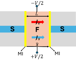
In the mesoscopic S/F/S junction (Fig. 1), the diffusion of the superconducting condensate into the F can be computed by using the Usadel equation [19], which provides a very satisfactory description in the typically experimentally relevant quasiclassical limit. The Usadel equation in F reads
| (1) |
in which represents the retarded component of the Green function, is the diffusion coefficient, , and represents the quasiparticle energy. The magnetization matrix is given by , where is the ferromagnetic exchange field and is the Pauli matrix vector. On the other hand, the two S electrodes are considered as reservoirs with the Usadel equation , in which . denotes the superconducting gap and we take it to be for the two S layers with being the gap amplitude and the phase difference. The solution of simply takes the standard Bardeen-Cooper-Schrieffer (BCS) bulk form.
To solve in Eq. (1), the boundary conditions at the S/F interfaces are required. Here the spin-active tunneling boundary condition introduced by a magnetic interface (e.g., spin-polarized magnetic insulator) between S and F layers is described as [20, 21, 22]
| (2) | |||
| (3) |
in which for the left (L) S/F interface while for the right (R) F/S interface. is the F length and denotes its bulk conductance. Other involved parameters include the interfacial tunneling conductance , spin-mixing conductance and polarization . The interfacial magnetization is given by with and . The notation is used for the magnetization of the L (R) interface. Next, we apply the Riccati parametrization [23, 24] for the quasiclassical Green function with to solve numerically with higher computation efficiency. To model inelastic scattering, a small imaginary part is added to the quasiparticle energies with .
The charge supercurrent flowing between the superconducting electrodes can in general be expressed as energy integrals of the charge spectral current in F:
| (4) |
where with being the density of states at the Fermi level and the interfacial contact area. Moreover, is the Green function matrix in Keldysh space given by Here, is the advanced component of the Green function which satisfies . As for the Keldysh component , it is also related to the non-equilibrium distribution matrix by . In our S/F/S system, a gate voltage is applied transversely across the F which drives the system out-of-equilibrium by manipulating the occupation states of electrons and holes with the distribution function [25, 26]
| (5) |
where . This relation is valid near the center of the voltage-biased F. Before coming to our main results on the spin-polarized diode effect, we first briefly examine at the charge supercurrent diode properties of the system.
Charge diode effect. – The nonreciprocity of charge supercurrent or charge SDE refers to the maximum charge supercurrent in one direction being different from the maximum charge supercurrent in the other direction, which can be mathematically expressed in terms of the charge current-phase relation . Here the charge SDE efficiency is defined as
| (6) |
where with () representing the phase at which achieves its maximum (minimum). In the absence of charge SDE, such as for a purely sinusoidal current-phase relation applies, .
It is known that the diode effects are governed by symmetry properties. The charge SDE investigated here in general requires that symmetries related to time-reversal and parity (inversion) are broken. In our S/F/S system, the magnetization or exchange field in the F forms a spin chirality with the two interfacial magnetizations of the spin-active S/F interfaces according to . A nonzero combined with the broken spin-degeneracy satisfies the symmetry requirements for possible diode effect, as is a pseudoscalar that is odd under parity (and time-reversal), since the parity operation exchanges and . To maximize three magnetizations orthogonal to each other are considered, i.e., , and . Except for the symmetry-breaking chirality, a gate voltage is applied to change the occupation of charge-supercurrent-carrying states in F, which importantly provides a purely electrical way of controlling the charge SDE.
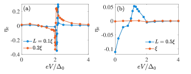
In Fig. 2, we investigate the charge SDE efficiency as a function of the applied electric voltage for different junction lengths. It is found a large magnitude of exceeding can be achieved for short junctions (e.g., with being the superconducting coherence length) by tuning , where a sharp jump along with a sign reversal appears at around is observed. In general, this jump can be understood by considering the voltage-controllable distribution function in Eq. (5), which corresponds to a characteristic two-step profile of the occupation of states as a function of energy . At , the two steps or jumps in occur at . On the other hand, the solution of approaches with the form proportional to when the F length is small, and therefore takes the typical superconducting coherence peaks at . As a result, the sharp jump at disappears for longer lengths as shown in Fig. 2(b), where the charge SDE becomes negligible for . Due to the mechansim described above, we will later see that the spin SDE also has a characteristic behavior for which is robust against variations in other parameters.
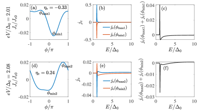
To explain the sign reversal of at , we then focus on two typical voltages and for , at which minimum () and maximum () are achieved, respectively. According to the definition of in Eq. (6), we first plot the charge current-phase relation to find and in Fig. 3(a) for and Fig. 3(d) for . Next, the charge spectral current at and are plotted separately, both of which show typical coherence peaks at , corresponding to the typical spectral current behavior of bulk superconductors. It can be seen that the peak value of has opposite signs for and . Since the sign of is determined by , we plot its corresponding integrand in Fig. 3(c) and Fig. 3(f). By comparing the area which represents the integral, we finally get in Fig. 3(c) for and in Fig. 3(f) for .
Except for the length dependence, we have also investigated other parameter dependences of for (see SM for details). We find that a larger peak magnitude of generally occurs at values of around 5-10 meV (as experimentally realized in e.g. PdNi [27] and CuxNi1-x [28]), as well as rather small values of the interface polarization , tunneling conductance and mixing conductance , based on the numerical analysis we have performed. The voltage-tunable sign reversal of with a peak magnitude of at least nevertheless remains robust against changes in the above parameters.
Spin diode effect. – Along with the charge supercurrent , there is spin supercurrent flowing in the junction which depends on the superconducting phase difference . The latter is controlled either via an applied charge current through the system or via a magnetic flux in a loop geometry. Consider the maximized configuration as introduced before, we have which polarized along the exchange field in the F. Similar to , can be calculated by integrating its corresponding spectral current as
| (7) |
in which , so that the spin supercurrent is polarized along . The coefficient is obtained by replacing with in .
Here we introduce and compute the spin-polarization of the charge supercurrent diode effect or spin SDE, whose efficiency is defined and characterized via the spin supercurrent evaluated at and as follows:
| (8) |
This parameter measures the difference in spin-polarization between the maximum charge supercurrent flow in each direction in the junction. We underline that this is a different definition than the one very recently proposed in Ref. [15], where the efficiency was defined as the difference in maximum spin-current flowing in each direction. The difference between these definitions is important with respect to the actual measurements of the SDE, and we argue that our definition is experimentally more feasible. The reason for this is that the phases are readily applied to the junction since they correspond to the largest charge current-bias that does not generate a voltage drop, i.e. the critical charge supercurrent. Our definition of then expresses what the spin-polarization is of the current flowing through the system when it is biased to have maximum charge transport in the left vs. right direction. This is different from identifying the phase differences providing the maximal spin supercurrent flow in each direction, which cannot experimentally be identified by current-biasing the system, as is normally done. Note here that () have the same definition as introduced before for , corresponding to the phase at which achieves maximum (minimum).
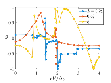
In Fig. 4, is plotted as a function of the applied voltage for different junction lengths. Consider smaller junction lengths (e.g., and ) first. Similar to shown in Fig. 2, a sharp jump is observed at around . Additionally, a sign reversal is obtained at smaller voltage . It is found that much larger magnitude exceeding can be achieved for both positive and negative values. Note that even the ideal efficiency is realizable by tuning the applied voltage, which occurs at around for . This ideal value means that the system completely forbids spin transport in one direction whereas it transport spins with zero energy loss in the other direction. As for larger length , a jump also exists at where almost approaches . Moreover, the ideal (both positive and negative) can also appear at voltage . This is distinctively different from that becomes negligible for the same length as shown in Fig. 2(b), such that and can differ greatly in magnitude for a given parameter set, indicating independent behavior.
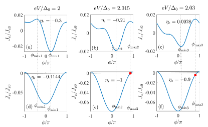
To determine the underlying physics of the ideal spin SDE efficiency, we focus on appearing at for as an example and compare the and cases which closely fall around it. In Fig. 5, we plot the corresponding charge current-phase relations under the above three applied voltages in the first row to find the corresponding and which are used to calculate through the spin current-phase relation in the second row. By comparing the charge current-phase relations, it can be seen that even when the voltage only slightly changes the charge supercurrent-phase relation, this is sufficient to cause an obvious change in . When the new is changed to a value where the spin supercurrent vanishes, we get , indicating that is fully polarized along one specific direction while absent along the other direction. Note here the large change of also ensures a large absolute change in the spin supercurrent magnitude.
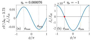
As for the ideal obtained at longer length (e.g., ) where the charge SDE is negligible, another mechanism plays a role to explain this phenomenon. This is shown in Fig. 6. In this case, deviates slightly from (based on the sinusoidal charge supercurrent-phase relation with zero ) but this change is enough to cause a notable change in . This is because of the behavior of the spin supercurrent at which emerges as becomes large, so that both or provide a small magnitude of . This allows the spin diode efficiency to become 100% for voltages that cause to vanish for either or . This indicates that a charge current-phase relation deviating from its standard form is not necessary to realize the ideal spin SDE: just a conventional -like behavior of the charge current-phase relation is enough, so long that the system also permits a spin supercurrent which goes like and can become zero under the small phase shifts from the ideal behavior in . Compared to the previous mechanism applied for shorter junction, the supercurrent change magnitude is limited by the small phase shift.
We have also investigated the robustness of the spin SDE against different parameter variations (see SM for details). We find that the ideal SDE remains robust against moderate variations in , , , , as well as the chirality (meaning that , and are not fully perpendicular to each other). The above robustness towards different parameter variations further facilitates experimental observation of spin SDE with reaching proposed in our work.
Conclusion. – In summary, we predict two mechanisms which make it possible to generate an electrically tunable spin-diode effect with ideal efficiency by using superconductor/ferromagnet multilayers. The system completely forbids spin transport in one direction whereas it transport spins with zero energy loss in the other direction. This result provides a way to integrate the superconducting diode effect with spin-polarized currents.
This work was supported by the Research Council of Norway through Grant No. 323766 and its Centres of Excellence funding scheme Grant No. 262633 “QuSpin.” Support from Sigma2 - the National Infrastructure for High Performance Computing and Data Storage in Norway, project NN9577K, is acknowledged.
References
- Ando et al. [2020] F. Ando, Y. Miyasaka, T. Li, J. Ishizuka, T. Arakawa, Y. Shiota, T. Moriyama, Y. Yanase, and T. Ono, Observation of superconducting diode effect, Nature 584, 373 (2020).
- Nadeem et al. [2023] M. Nadeem, M. S. Fuhrer, and X. Wang, The superconducting diode effect, Nat. Rev. Phys. 5, 558 (2023).
- Wu et al. [2022] H. Wu, Y. Wang, Y. Xu, P. K. Sivakumar, C. Pasco, U. Filippozzi, S. S. P. Parkin, Y.-J. Zeng, T. McQueen, and M. N. Ali, The field-free Josephson diode in a van der Waals heterostructure, Nature 604, 653 (2022).
- Pal et al. [2022] B. Pal, A. Chakraborty, P. K. Sivakumar, M. Davydova, A. K. Gopi, A. K. Pandeya, J. A. Krieger, Y. Zhang, M. Date, S. Ju, N. Yuan, N. B. M. Schröter, L. Fu, and S. S. P. Parkin, Josephson diode effect from Cooper pair momentum in a topological semimetal, Nat. Phys. 18, 1228 (2022).
- Trahms et al. [2023] M. Trahms, L. Melischek, J. F. Steiner, B. Mahendru, I. Tamir, N. Bogdanoff, O. Peters, G. Reecht, C. B. Winkelmann, F. von Oppen, and K. J. Franke, Diode effect in Josephson junctions with a single magnetic atom, Nature 615, 628 (2023).
- Hu et al. [2023] J.-X. Hu, Z.-T. Sun, Y.-M. Xie, and K. T. Law, Josephson Diode Effect Induced by Valley Polarization in Twisted Bilayer Graphene, Phys. Rev. Lett. 130, 266003 (2023).
- Costa et al. [2023a] A. Costa, J. Fabian, and D. Kochan, Microscopic study of the Josephson supercurrent diode effect in Josephson junctions based on two-dimensional electron gas, Phys. Rev. B 108, 054522 (2023a).
- Pillet et al. [2023] J.-D. Pillet, S. Annabi, A. Peugeot, H. Riechert, E. Arrighi, J. Griesmar, and L. Bretheau, Josephson diode effect in Andreev molecules, Phys. Rev. Res. 5, 033199 (2023).
- Hodt and Linder [2023] E. W. Hodt and J. Linder, On-off switch and sign change for a nonlocal Josephson diode in spin-valve Andreev molecules, Phys. Rev. B 108, 174502 (2023).
- Costa et al. [2023b] A. Costa, C. Baumgartner, S. Reinhardt, J. Berger, S. Gronin, G. C. Gardner, T. Lindemann, M. J. Manfra, J. Fabian, D. Kochan, N. Paradiso, and C. Strunk, Sign reversal of the Josephson inductance magnetochiral anisotropy and 0–-like transitions in supercurrent diodes, Nat. Nanotechnol. 18, 1266 (2023b).
- Lotfizadeh et al. [2024] N. Lotfizadeh, W. F. Schiela, B. Pekerten, P. Yu, B. H. Elfeky, W. M. Strickland, A. Matos-Abiague, and J. Shabani, Superconducting diode effect sign change in epitaxial Al-InAs Josephson junctions, Commun. Phys. 7, 1 (2024).
- Zazunov et al. [2024] A. Zazunov, J. Rech, T. Jonckheere, B. Grémaud, T. Martin, and R. Egger, Nonreciprocal charge transport and subharmonic structure in voltage-biased Josephson diodes, Phys. Rev. B 109, 024504 (2024).
- Lu et al. [2023] B. Lu, S. Ikegaya, P. Burset, Y. Tanaka, and N. Nagaosa, Tunable Josephson Diode Effect on the Surface of Topological Insulators, Phys. Rev. Lett. 131, 096001 (2023).
- Gupta et al. [2023] M. Gupta, G. V. Graziano, M. Pendharkar, J. T. Dong, C. P. Dempsey, C. Palmstrøm, and V. S. Pribiag, Gate-tunable superconducting diode effect in a three-terminal Josephson device, Nat. Commun. 14, 1 (2023).
- Mao et al. [2024] Y. Mao, Q. Yan, Y.-C. Zhuang, and Q.-F. Sun, Universal Spin Superconducting Diode Effect from Spin-Orbit Coupling, Phys. Rev. Lett. 132, 216001 (2024).
- Mackenzie and Maeno [2003] A. P. Mackenzie and Y. Maeno, The superconductivity of and the physics of spin-triplet pairing, Rev. Mod. Phys. 75, 657 (2003).
- Pustogow et al. [2019] A. Pustogow, Y. Luo, A. Chronister, Y.-S. Su, D. A. Sokolov, F. Jerzembeck, A. P. Mackenzie, C. W. Hicks, N. Kikugawa, S. Raghu, E. D. Bauer, and S. E. Brown, Constraints on the superconducting order parameter in Sr2RuO4 from oxygen-17 nuclear magnetic resonance, Nature 574, 72 (2019).
- Golubov et al. [2004] A. A. Golubov, M. Y. Kupriyanov, and E. Il’ichev, The current-phase relation in Josephson junctions, Rev. Mod. Phys. 76, 411 (2004).
- Usadel [1970] K. D. Usadel, Generalized diffusion equation for superconducting alloys, Phys. Rev. Lett. 25, 507 (1970).
- Konstandin et al. [2005] A. Konstandin, J. Kopu, and M. Eschrig, Superconducting proximity effect through a magnetic domain wall, Phys. Rev. B 72, 140501 (2005).
- Ouassou and Linder [2019] J. A. Ouassou and J. Linder, Voltage control of superconducting exchange interaction and anomalous Josephson effect, Phys. Rev. B 99, 214513 (2019).
- Ouassou et al. [2017] J. A. Ouassou, A. Pal, M. Blamire, M. Eschrig, and J. Linder, Triplet Cooper pairs induced in diffusive s-wave superconductors interfaced with strongly spin-polarized magnetic insulators or half-metallic ferromagnets, Sci. Rep. 7, 1 (2017).
- Schopohl and Maki [1995] N. Schopohl and K. Maki, Quasiparticle spectrum around a vortex line in a d-wave superconductor, Phys. Rev. B 52, 490 (1995).
- Schopohl [1998] N. Schopohl, Transformation of the Eilenberger Equations of Superconductivity to a Scalar Riccati Equation, arXiv 10.48550/arXiv.cond-mat/9804064 (1998), cond-mat/9804064 .
- Wilhelm et al. [1998] F. K. Wilhelm, G. Schön, and A. D. Zaikin, Mesoscopic Superconducting–Normal Metal–Superconducting Transistor, Phys. Rev. Lett. 81, 1682 (1998).
- Heikkilä et al. [2000] T. T. Heikkilä, F. K. Wilhelm, and G. Schön, Non-equilibrium supercurrent through mesoscopic ferromagneticweak links, Europhys. Lett. 51, 434 (2000).
- Kontos et al. [2002] T. Kontos, M. Aprili, J. Lesueur, F. Genêt, B. Stephanidis, and R. Boursier, Josephson junction through a thin ferromagnetic layer: Negative coupling, Phys. Rev. Lett. 89, 137007 (2002).
- Ryazanov et al. [2001] V. V. Ryazanov, V. A. Oboznov, A. Y. Rusanov, A. V. Veretennikov, A. A. Golubov, and J. Aarts, Coupling of two superconductors through a ferromagnet: Evidence for a junction, Phys. Rev. Lett. 86, 2427 (2001).