Engineering Si-Qubit MOSFETs: A Phase-Field Modeling Approach Integrating Quantum-Electrostatics at Cryogenic Temperatures
Abstract
This study employs advanced phase-field modeling to investigate Si-based qubit MOSFETs, integrating electrostatics and quantum mechanical effects. We adopt a comprehensive modeling approach, utilizing full-wave treatment of the Schrödinger equation solutions, coupled with the Poisson equation at cryogenic temperatures. Our analysis explores the influence of interface traps on quantum dot (QD) barrier heights, affecting coupling due to tunneling. A wider trap distribution leads to the decoupling of quantum dots. Furthermore, the oscillations in the transmission & reflection coefficients increase as the plunger/barrier gate length is increased, reducing the coupling between the QDs. By optimizing plunger and barrier gate dimensions, spacer configurations, and gap oxide lengths, we enhance control over quantum well depths and minimize unwanted wave function leakage. The modeling algorithm is also validated against the experimental data and can accurately capture the oscillations in the caused by the Coulomb blockade at cryogenic temperature.
I Introduction
Silicon-based qubit devices present exceptional scalability, targeting the future needs of millions of qubits for practical quantum computing [1], [2], [3], [4]. The electronics part of Si-based qubit systems has been discussed by Zwanenburg et. al. [1]. Recent advancements in Si and SiGe quantum devices demonstrate exceptionally high low-temperature mobility [5], a six-bit quantum processor [6], scalable silicon quantum processor design using flip-flop qubit [7], greater than 0.1 ms relaxation times [8], [9], silicon quantum dots with sufficient thermal robustness to perform universal gate is demonstrated in [10], quantum-state foundation as a tomography to characterize entanglement [11], two-bit CNOT Qubit logic gate [12], FinFET based Si-qubit [13], 22-nm FD SOI based single-electron injection qubit device [14], and high fidelity silicon-based qubit [15], [16], [17].
There have been significant advancements in the qubit simulation and modeling domain. Dynamical mean-field theory for qubit [18], variational hybrid algorithm by using both classical and quantum physics [19], utilizing molecular wave function to study qubit [20], quantum monte-carlo simulations [21], first principle based simulations to analyze the nano-scale physics of qubit [22], [23], [24] quantum simulation using fermionic swap network [25], quantum imaginary time technique to determine eigen energies [26], The physics of point defect and its impact on qubit is explored via experimental or simulations [27], [28], [29], quantum phase transition [30], quantum embed algorithm to simulate quantum computer [31], 2- D material impact on qubit spin and electrostatics [32], [33], [34].
From the large circuit perspective. Recently, a 3-D integration of a Si-qubit circuit was demonstrated in [35], [36], [37]. A large-scale circuit such as the electronic controller was reported in [38], On-chip switch capacitor integration in [39], and a 28-nm node pulse modulator in [40]. The recent good review articles discuss the advancement in qubit-based electronics from devices to circuits [41], [42]. A recent study by Mohiyaddin et al. developed a multiphysics modeling algorithm to study Si-qubit devices [43]. However, the authors did not consider a full wave treatment, and the WKB approximation was used to calculate the tunnel coupling. The overlap of wave functions among qubits is crucial for achieving multi-state storage, superposition, and thoroughly understanding the electrostatics [1], [4]. Therefore, a detailed microscopic understanding of electron wave function interactions, tunneling, and exchange coupling is vital for efficient quantum computer development. Additionally, Mohiyaddin et al. work did not consider the impact of trap distribution and plunger/barrier gate on the qubit device.

In this work, we introduce a phase-field modeling framework for Si-based qubit MOSFETs using three different physics modules in COMSOL [44]. This framework employs a full-wave treatment of electrons at cryogenic temperatures, which solves the 2-D Poisson equation, coupled with the tine-independent Schrodinger equation. Using incident, reflected, and transmitted wave functions, we calculate tunneling and exchange coupling. Additionally, we examine the impact of SiO2/Si surface trap distributions on qubit performance. We optimize the plunger gate, barrier gate, gap oxide, gate oxide, and spacer oxide to enhance the tunneling and exchange coupling among quantum dots.
The following approximations are made in this work.
1) We do not consider the magnetic field in this modeling, as this work aims to analyze the electrostatics part of the qubit. 2) We do not include the impact of external noise, coherence, and dephasing. An accurate incorporation of spin effects, noise and coherence requires solving the time-dependent Schrödinger equation with a full Hamiltonian (including magnetic component) converging at cryogenic temperatures, which is beyond the scope of this work. We consider a 2-D geometry which is also experimentally reported in the recent study by Intel, a Si-bulk MOSFET was used to build a qubit device [5]. A 2-D structure leads to better convergence and reliable results. For the 3-D system, one needs to solve 2-D Schrödinger with 3-D Poisson’s including wave treatment which might not lead to a stable simulation platform. Furthermore, the device electrostatic such as the impact of gate field, oxide thickness, and trap impact will follow a similar trend in 3-D as in the 2-D structure.
We analyze the electrostatics part of a small qubit device and engineer the core device for optimal tunnel coupling and electrostatic integrity. This study can help to understand the fundamental ways to optimize and design an efficient qubit for a strong tunnel and exchange coupling.
II Methodology
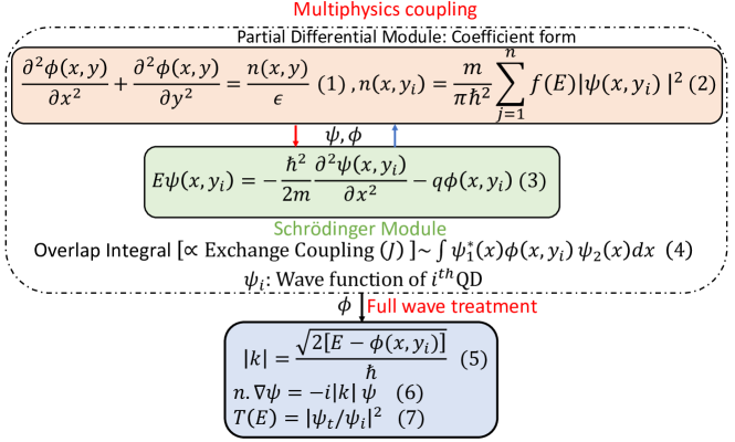
Fig. 1 depicts the schematic of a Si-based qubit MOSFET featuring two quantum dots (QD). Our earlier work used the COMSOL Multiphysics module can be used to model complex partial differential equations in semiconductor physics [45], [46]. Fig. 2 illustrates the phase-field modeling algorithm utilized in this study. We integrated three different physics modules within COMSOL using the Multiphysics tool.
II.1 Coefficient form Partial Differential Equation Module: Poisson’s Equation
The 2-D Poisson’s equation was implemented in the Coefficient from the Partial Differential Equation (PDE) module of the COMSOL. The electron charge density was calculated from the wave function and Fermi-Dirac distribution (Eq. 3). The wave function () and potential function () are defined as dependent variables that are fed back into the Schrödinger module.
II.2 Schrödinger Module-1: SCHRP Solver
The COMSOL has an inbuilt Schrödinger module which can be used to calculate the eigen energy and wave function. There are two key steps for the convergence at cryogenic temperatures:
-
1.
Initially a Gaussian wave function is assumed which is given as an input in the initial value of the Schrödinger Module. This initial function is defined in the analytical function section and then used in the initial value section of the Schrödinger Module. Therefore, this approximation helps the tool to begin with the initial data points to move towards convergence.
-
2.
First we obtain the solution at 200 K in a separate stationary study, which is fed back into the Values of Dependent Variable section of the cryogenic study ( 10 K). This step provides the initial potential function, charge densities, and wave function to start the cryogenic analysis.
-
3.
Subsequently, the dependent variables potential and are plugged into the electron potential energy section and dependent variable section of the PDE module, respectively. An iterative procedure is used till convergence is achieved.
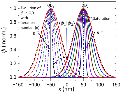
The iterative solution of Schrödinger and Poisson’s solver (SCHRP) evolves the wave function () as shown in Fig. 3. Approximately after 60-65 iterations wave function begins to converge. One might need to change the maximum number of iteration limits in the study section to obtain the correct convergence.
II.3 Schrödinger Module-2: Full Wave Treatment
Once we obtain convergence in potential and wave function from the last step, it can be stated that for the given terminal voltages and device physical parameters an accurate potential distribution is obtained at 10 K. The obtained is then used in the Electron Potential Energy section of the second 1-D Schrödinger Module to calculate the transmission and reflection coefficient following the exact wave treatment. This acts as the electron potential (or barrier) in determining the transmission/reflection coefficients. COMSOL computes the wave number following Eq. (5), and spatial variation in the wave function with respect to space dimension is calculated from Eq. (6). In the last step the transmission coefficient at each energy step is evaluated by analyzing the transmitted and incident wave magnitude. For simplicity, the tool assumes an initial incident wave magnitude = 1, which evolves with iterations [44].
II.4 Dependent Variable Transfer between Various Modules
As explained previously in the above steps the dependent variable transfer is an important step to accurately couple all the modules which can be summarized as:
-
1.
PDE: define & as the dependent variable in the Coefficient form PDE module under the declaration section.
-
2.
Schrödinger module-1 : Transfer in the electron potential energy section and in the module dependent variable section. Obtain an iterative solution with a proper initial guess (wave function) and solution ( 200 K) [see above steps for detail].
-
3.
The obtained from the above steps is used in the second Schrödinger module to calculate transmission and reflection coefficients with full wave treatment.
III MODEL VALIDATION
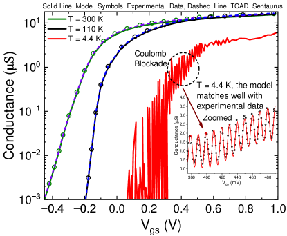
Fig. 4 shows the model validations with experimental data reported in [47]. The oscillations in the model have a regular period given by , where is the gate capacitance. The model correctly predicts the temperature dependence, with more pronounced oscillations at lower temperatures due to the reduction in thermal energy overcoming the Coulomb energy barriers, demonstrating its capability to capture single-electron effects characteristic of Coulomb blockade. Furthermore, we also validate the model with standard TCAD Sentaurus [48], proving the additional robustness of the developed phase-field model.
Note the data in [47] is reported for nano-wire, but the cross-section is a 2-D structure, as shown in Fig. 1, leading to matching with the simulations for K. At cryogenic temperature (4.4 K), a mismatch is observed. However, the simulations still follow the trends capturing oscillations in the which is enough to justify the model validity. For validation purposes we use the same parameters, as given in [47].
IV INTERFACE TRAP and QUBIT PERFORMANCE
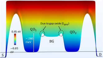
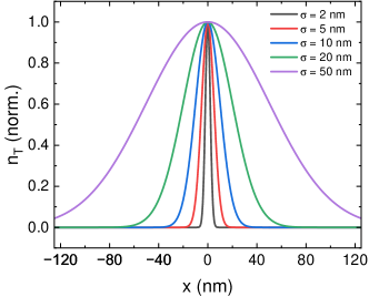
Fig. 5 shows the 2-D surface plot of conduction band energy for negligible trap density. The QD’s well depth is 280 meV. The local humps near the well boundary are due to the fringing from gap-oxides (Lgap). A neutral point defect (trap) is included by assuming the trap’s spatial distribution as a Gaussian with peak concentration 81010cm-2, generally observed in a good interface [49]. Assuming a Gaussian trap distribution is widely used to simulate/model the impact of interface trap density [50], [51], Fig. 6 shows the typical normalized interface trap distribution centered at the mid-channel for the various variance values.
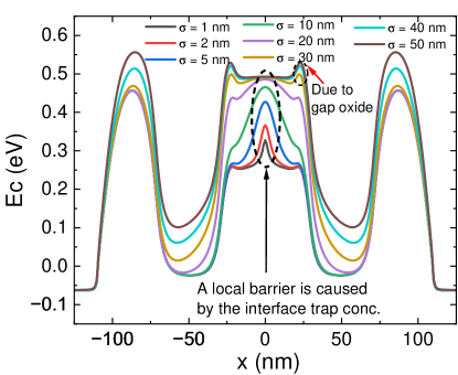
Since the interface traps are generally electron traps,[49] these traps possess a negative charge when occupied, leading to a local increase in the barrier height of the quantum dot. Fig. 7 plotted at Si/SiO2 interface considers a Gaussian distribution of traps of the fixed peak but standard deviation varying from 1 nm to 50 nm. An increasing increases the total trap charge density, i.e., . Here is the trap distribution area which increases with , leading to an enhancement in the total trap charge and increasing barrier height, until the trap distribution covers the whole channel region, causing the saturation for 40 nm.
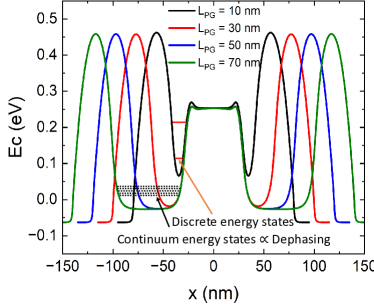
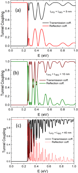
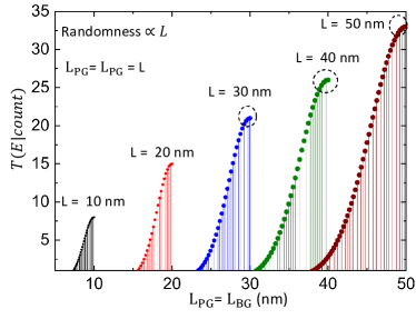
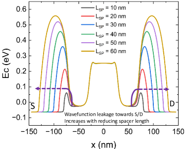
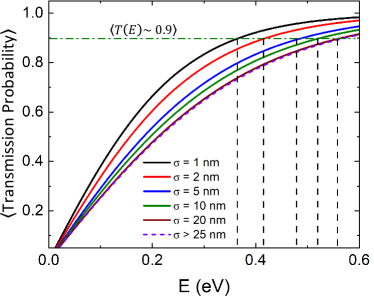
Fig. 8 shows the impact of trap distribution on the average tunnel coupling of the quantum dots. The increasing barrier height caused by the higher reduces the tunnel coupling. Furthermore, the energy maxima at which T(E) 0.9 increases with barrier height. Therefore, the energy required (gate voltage) to strongly couple such quantum dots will increase with the broader trap distribution.
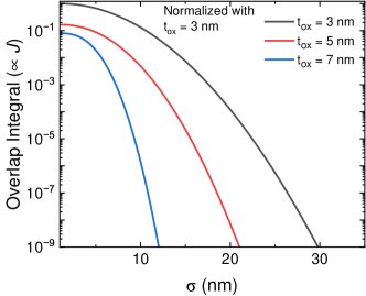
The impact of trap distribution on exchange coupling is shown in Fig. 9. Increasing barrier height reduces the wave function’s overlap integral , leading to a reduction in the exchange coupling. Furthermore, the thicker the gate oxide, the weaker the plunger and barrier gate control, further reducing the exchange coupling.
V PLUNGER and BARRIER GATE ENGINEERING
Fig. 10 shows the impact of plunger gate length (LPG) on the quantum well. The quantum well depth shows a negligible dependency for L 30 nm. However, the well depths decrease at the smaller plunger gate lengths. At a very small value of L 10 nm, the eigen-energy separation between dot electrons is exceptionally high . Therefore, there are only a few available states at which quantum dots can interact with each other.
Fig. 11(a) shows the transmission probability for plunger (LPG) and barrier (LBG) gate length = 5 nm. Due to the very high only two modes (energy states) are available, leading to small oscillations in the overlap integral and T(E). The increasing value of LPG (LBG) reduces the causing a continuum of energy states, which significantly increases the oscillations in the T(E), as shown in (b) & (c). This increase in oscillations increases the likelihood of unintended electron transitions between states, leading to randomness in the tunnel coupling, as shown in Fig. 12. The randomness is calculated as the number of oscillations in the transmission coefficient till it saturates with respect to energy. The variance of randomness also increases with LPG.
VI SPACER and GAP OXIDE ENGINEERING
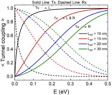
Fig. 13 shows the conduction band profile of the quantum wells for various source/drain spacer lengths (LSP). For the L 30 nm, the source/drain depletion region begins to alter the well depths. At very small L 10 nm, the quantum well begins to disappear due to the degeneracy of S/D, and the region below the plunger gates is now controlled by the S/D depletion width. Its impact on tunnel coupling is shown in Fig. 14. For LSP = 10 nm, almost the entire wave function of dot electron is transmitted towards the source and drain side from QD1 and QD2, respectively. At LSP = 15 nm, almost 50% of the electron wave function diffuses towards S/D. For L 30 nm, there is 8 % leakage of wave function towards S/D, and almost the entire quantum well is controlled by the plunger/barrier gates. Therefore, keeping a larger S/D drain spacer can help to enhance quantum dot coupling.
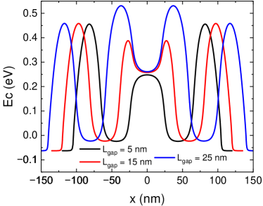
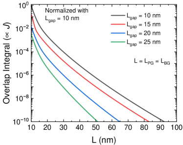
Fig. 15 shows the interface conduction band energy (QD) for the various gap oxide lengths (Lgap). Here Lgap is the oxide gap length between adjacent plunger/barrier gates (see Fig. 1). The increasing value of Lgap induces corner humps in the barrier due to the local fringing fields. These local humps increase the barrier height of the quantum wells. At very large Lgap, it might be possible that wells do not interact with each other due to a very large potential barrier. Fig. 16 shows the exchange coupling for the various gap lengths. Increasing Lgap reduces exchange coupling due to decreased overlap between the electron wave functions.
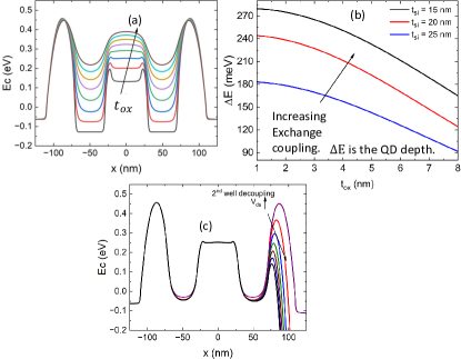
Fig. 17(a) shows the impact of gate oxide thickness on quantum dots. Increasing gate oxide thickness reduces the gate control and well depths, which reduces the exchange coupling. The increasing value of silicon film thickness also reduces the quantum well depths due to reduced gate control, as shown in Fig. 17(b). An increasing drain voltage value causes drain-induced barrier lowering, reducing the quantum well depth near the drain side, as shown in Fig. 17(c), which will decrease the exchange and tunnel coupling.
Fig. 18 shows the Summary of this work: The coupling is maximized at an intermediate barrier/plunger gate length. Too small or too large spacer lengths reduce the coupling. When the oxide gap is very small, the quantum wells merge, resulting in zero coupling, and at very large oxide gaps, coupling also decreases. Increasing the gate oxide thickness and the Si film thickness decreases the coupling.

VII Conclusion
We have elucidated critical factors affecting Si-based qubit MOSFET performance by integrating electrostatics, quantum mechanics, and magnetic effects, including full wave treatment of electrons at cryogenic temperatures. Our findings highlight the significant impact of interface traps on barrier heights which influence tunnel coupling. Optimal engineering of plunger and barrier gates, spacer widths, and gap oxide lengths was shown to enhance quantum well depth control and minimize unwanted wave leakage, increasing the coupling and electrostatic integrity.
References
- [1] F. A. Zwanenburg, A. S. Dzurak, A. Morello, M. Y. Simmons, L. C. L. Hollenberg, G. Klimeck, S. Rogge, S. N. Coppersmith, and M. A. Eriksson, ”Silicon quantum electronics,” Rev. Mod. Phys., vol. 85, no. 3, pp. 961-1019, Jul. 2013. doi: 10.1103/RevModPhys.85.961.
- [2] R. Maurand, X. Jehl, D. Kotekar-Patil, A. Corna, H. Bohuslavskyi, R. Lavi´eville, L. Hutin, S. Barraud, M. Vinet, M. Sanquer, and S. De Franceschi, A cmos silicon spin qubit, Nature Communications 7, 13575 (2016), doi: 10.1038/ncomms13575
- [3] P. Harvey-Collard, R. M. Jock, N. T. Jacobson, A. D. Baczewski, A. M. Mounce, M. J. Curry, D. R. Ward, J. M. Anderson, R. P. Manginell, J. R. Wendt, M. Rudolph, T. Pluym, M. P. Lilly, M. Pioro-Ladri‘ere, and M. S. Carroll, All-electrical universal control of a double quantum dot qubit in silicon mos, in 2017 IEEE International Electron Devices Meeting (IEDM) (2017) pp. 36.5.1–36.5.4, doi:10.1109/IEDM.2017.8268507.
- [4] J. H. Davies, Tunnelling transport, in The Physics of Low-dimensional Semiconductors: An Introduction (Cambridge University Press, 1997) p. 150–205.
- [5] R. Pillarisetty, T. Watson, B. Mueller, E. Henry, H. George, S. Bojarski, L. Lampert, F. Luthi, R. Kotlyar, O. Zietz, S. Neyens, F. Borjans, R. Caudillo, D. Michalak, R. Nahm, J. Park, M. Ramsey, J. Roberts, S. Schaal, G. Zheng, T. Kr¨ahenmann, M. Lodari, A. Zwerver, M. Veldhorst, G. Scappucci, L. Vandersvpen, and J. Clarke, Si mos and si/sige quantum well spin qubit platforms for scalable quantum computing, in 2021 IEEE International Electron Devices Meeting (IEDM) (2021) pp. 14.1.1–14.1.4, doi: 10.1109/IEDM19574.2021.9720567.
- [6] S. G. J. Philips, M. T. Madzik, S. V. Amitonov, S. L. de Snoo, M. Russ, N. Kalhor, C. Volk, W. I. L. Lawrie, D. Brousse, L. Tryputen, B. P. Wuetz, A. Sammak, M. Veldhorst, G. Scappucci, and L. M. K. Vandersypen, Universal control of a six-qubit quantum processor in silicon, Nature 609, 919 (2022), doi: 10.1038/s41586-022 05117-x.
- [7] G. Tosi, F. A. Mohiyaddin, V. Schmitt, S. Tenberg, R. Rahman, G. Klimeck, and A. Morello, Silicon quantum processor with robust long-distance qubit couplings, Nature Communications 8, 450 (2017), doi: 10.1038/s41467-017-00378-x.
- [8] J. Verjauw, R. Acharya, J. Van Damme, T. Ivanov, D. P. Lozano, F. A. Mohiyaddin, D. Wan, J. Jussot, A. M. Vadiraj, M. Mongillo, M. Heyns, I. Radu, B. Govoreanu, and A. Potoˇcnik, Path toward manufacturable superconducting qubits with relaxation times exceeding 0.1 ms, npj Quantum Information 8, 93 (2022), doi: 10.1038/s41534-022-00600-9.
- [9] C. Wang, X. Li, H. Xu, Z. Li, J. Wang, Z. Yang, Z. Mi, X. Liang, T. Su, C. Yang, G. Wang, W. Wang, Y. Li, M. Chen, C. Li, K. Linghu, J. Han, Y. Zhang, Y. Feng, Y. Song, T. Ma, J. Zhang, R. Wang, P. Zhao, W. Liu, G. Xue, Y. Jin, and H. Yu, Towards practical quantum computers: transmon qubit with a lifetime approaching 0.5 milliseconds, npj Quantum Information 8, 3 (2022), doi: 10.1038/s41534-021-00510-2.
- [10] L. Petit, H. G. J. Eenink, M. Russ, W. I. L. Lawrie, N. W. Hendrickx, S. G. J. Philips, J. S. Clarke, L. M. K. Vandersypen, and M. Veldhorst, Universal quantum logic in hot silicon qubits, Nature 580, 355 (2020), doi: 10.1038/s41586-020-2170-7.
- [11] T. F. Watson, S. G. J. Philips, E. Kawakami, D. R. Ward, P. Scarlino, M. Veldhorst, D. E. Savage, M. G. Lagally, M. Friesen, S. N. Coppersmith, M. A. Eriksson, and L. M. K. Vandersypen, A programmable two-qubit quantum processor in silicon, Nature 555, 633 (2018), doi: 10.1038/nature25766.
- [12] M. Veldhorst, C. H. Yang, J. C. C. Hwang, W. Huang, J. P. Dehollain, J. T. Muhonen, S. Simmons, A. Laucht, F. E. Hudson, K. M. Itoh, A. Morello, and A. S. Dzurak, A two-qubit logic gate in silicon, Nature 526, 410 (2015), doi: 10.1038/nature15263.
- [13] A. Fuhrer, M. Aldeghi, T. Berger, L. C. Camenzind, R. S. Eggli, S. Geyer, P. Harvey-Collard, N. W. Hendrickx, E. Kelly, L. Massai, M. Mergenthaler, P. M¨uller, A. V. Kuhlmann, T. Patlatiuk, S. Paredes, F. J. Schupp, G. Salis, L. Sommer, K. Tsoukalas, N. V. Trivino, R. J. Warburton, and D. M. Zumb¨uhl, Spin qubits in silicon finfet devices, in 2022 International Electron Devices Meeting (IEDM) (2022) pp. 14.1.1–14.1.4.
- [14] I. Bashir, E. Blokhina, A. Esmailiyan, D. Leipold, M. Asker, E. Koskin, P. Giounanlis, H. Wang, D. Andrade-Miceli, A. Sokolov, A. Koziol, T. Siriburanon, and R. B. Staszewski, A single-electron injection device for cmos charge qubits implemented in 22-nm fdsoi, IEEE Solid-State Circuits Letters 3, 206 (2020), doi: 10.1109/LSSC.2020.3010822.
- [15] C. H. Yang, K. W. Chan, R. Harper, W. Huang, T. Evans, J. C. C. Hwang, B. Hensen, A. Laucht, T. Tanttu, F. E. Hudson, S. T. Flammia, K. M. Itoh, A. Morello, S. D. Bartlett, and A. S. Dzurak, Silicon qubit fidelities approaching incoherent noise limits via pulse engineering, Nature Electronics 2, 151 (2019), doi: 10.1038/s41928-019-0234-1.
- [16] W. Huang, C. H. Yang, K. W. Chan, T. Tanttu, B. Hensen, R. C. C. Leon, M. A. Fogarty, J. C. C. Hwang, F. E. Hudson, K. M. Itoh, A. Morello, A. Laucht, and A. S. Dzurak, Fidelity benchmarks for two-qubit gates in silicon, Nature 569, 532 (2019), doi: 10.1038/s41586- 019-1197-0.
- [17] A. R. Mills, C. R. Guinn, M. J. Gullans, A. J. Sigillito, M. M. Feldman, E. Nielsen, and J. R. Petta, Twoqubit silicon quantum processor with operation fidelity exceeding 99%, Science Advances 8, eabn5130 (2022), doi: 10.1126/sciadv.abn5130.
- [18] A. Georges, G. Kotliar, W. Krauth, and M. J. Rozenberg, Dynamical mean-field theory of strongly correlated fermion systems and the limit of infinite dimensions, Rev. Mod. Phys. 68, 13 (1996), doi: 10.1103/RevModPhys.68.13.
- [19] J. R. McClean, J. Romero, R. Babbush, and A. AspuruGuzik, The theory of variational hybrid quantumclassical algorithms, New Journal of Physics 18, 023023 (2016), doi: 10.1088/1367-2630/18/2/023023.
- [20] A. Aspuru-Guzik, A. D. Dutoi, P. J. Love, and M. Head-Gordon, Simulated quantum computation of molecular energies, Science 309, 1704 (2005), doi: 10.1126/science.1113479, https://www.science.org/doi/pdf/10.1126/science.1113479.
- [21] L. K. Wagner and D. M. Ceperley, Discovering correlated fermions using quantum monte carlo, Reports on Progress in Physics 79, 094501 (2016), doi: 10.1088/0034-4885/79/9/094501.
- [22] T. Zhu, Z.-H. Cui, and G. K.-L. Chan, Efficient formulation of ab initio quantum embedding in periodic systems: Dynamical mean-field theory, Journal of Chemical Theory and Computation 16, 141 (2020), doi: 10.1021/acs.jctc.9b00934.
- [23] Z.-H. Cui, T. Zhu, and G. K.-L. Chan, Efficient implementation of ab initio quantumembedding in periodic systems: Density matrixembedding theory, Journal of Chemical Theory and Computation 16, 119 (2020), doi: 10.1021/acs.jctc.9b00933.
- [24] T. Nguyen Lan, A. A. Kananenka, and D. Zgid, Rigorous ab initio quantum embedding for quantum chemistry using green’s function theory: Screened interaction, nonlocal self-energy relaxation, orbital basis, and chemical accuracy, Journal of Chemical Theory and Computation 12, 4856 (2016), doi: 10.1021/acs.jctc.6b00638.
- [25] I. D. Kivlichan, J. McClean, N. Wiebe, C. Gidney, A. Aspuru-Guzik, G. K.-L. Chan, and R. Babbush, Quantum simulation of electronic structure with linear depth and connectivity, Phys. Rev. Lett. 120, 110501 (2018).
- [26] M. Motta, C. Sun, A. T. K. Tan, M. J. O’Rourke, E. Ye, A. J. Minnich, F. G. S. L. Brand˜ao, and G. K.-L. Chan, Determining eigenstates and thermal states on a quantum computer using quantum imaginary time evolution, Nature Physics 16, 205 (2020), doi: 10.1038/s41567-019- 0704-4.
- [27] J. R. Weber, W. F. Koehl, J. B. Varley, A. Janotti, B. B. Buckley, C. G. V. de Walle, and D. D. Awschalom, Quantum computing with defects, Proceedings of the National Academy of Sciences 107, 8513 (2010), doi: 10.1073/pnas.1003052107.
- [28] V. Iv´ady, I. A. Abrikosov, and A. Gali, First principles calculation of spin-related quantities for point defect qubit research, npj Computational Materials 4, 76 (2018), doi: 10.1038/s41524-018-0132-5.
- [29] C.-W. Lee, M. Singh, A. C. Tamboli, and V. Stevanovi´c, Transition metal impurities in silicon: computational search for a semiconductor qubit, npj Computational Materials 8, 172 (2022), doi: 10.1038/s41524-022-00862-z.
- [30] X.-Y. Guo, C. Yang, Y. Zeng, Y. Peng, H.-K. Li, H. Deng, Y.-R. Jin, S. Chen, D. Zheng, and H. Fan, Observation of a dynamical quantum phase transition by a superconducting qubit simulation, Phys. Rev. Appl. 11, 044080 (2019), doi: 10.1103/PhysRevApplied.11.044080.
- [31] H. Ma, M. Govoni, and G. Galli, Quantum simulations of materials on near-term quantum computers, npj Computational Materials 6, 85 (2020).
- [32] M. Ye, H. Seo, and G. Galli, Spin coherence in twodimensional materials, npj Computational Materials 5, 44 (2019), doi: 10.1038/s41524-019-0182-3.
- [33] R. Babar, G. Barcza, A. Pershin, H. Park, O. Bulancea Lindvall, G. Thiering, O. Legeza, J. H. Warner, ¨ I. A. Abrikosov, A. Gali, and V. Iv´ady, Low-symmetry vacancy-related spin qubit in hexagonal boron nitride, npj Computational Materials 10, 184 (2024), doi: 10.1038/s41524-024-01361-z.
- [34] S. Mondal and A. Lunghi, Spin-phonon decoherence in solid-state paramagnetic defects from first principles, npj Computational Materials 9, 120 (2023), doi: 10.1038/s41524-023-01082-9.
- [35] M. Veldhorst, H. G. J. Eenink, C. H. Yang, and A. S. Dzurak, Silicon cmos architecture for a spin-based quantum computer, Nature Communications 8, 1766 (2017), doi: 10.1038/s41467-017-01905-6
- [36] D. Rosenberg, D. Kim, R. Das, D. Yost, S. Gustavsson, D. Hover, P. Krantz, A. Melville, L. Racz, G. O. Samach, S. J. Weber, F. Yan, J. L. Yoder, A. J. Kerman, and W. D. Oliver, 3d integrated superconducting qubits, npj Quantum Information 3, 42 (2017), doi: 10.1038/s41534- 017-0044-0.
- [37] D. R. W. Yost, M. E. Schwartz, J. Mallek, D. Rosenberg, C. Stull, J. L. Yoder, G. Calusine, M. Cook, R. Das, A. L. Day, E. B. Golden, D. K. Kim, A. Melville, B. M. Niedzielski, W. Woods, A. J. Kerman, and W. D. Oliver, Solid-state qubits integrated with superconducting through-silicon vias, npj Quantum Information 6, 59 (2020), doi: 10.1038/s41534-020-00289-8.
- [38] B. Patra, R. M. Incandela, J. P. G. van Dijk, H. A. R. Homulle, L. Song, M. Shahmohammadi, R. B. Staszewski, A. Vladimirescu, M. Babaie, F. Sebastiano, and E. Charbon, Cryo-cmos circuits and systems for quantum computing applications, IEEE Journal of Solid-State Circuits 53, 309 (2018), doi: 10.1109/JSSC.2017.2737549.
- [39] Y. Xu, F. K. Unseld, A. Corna, A. M. J. Zwerver, A. Sammak, D. Brousse, N. Samkharadze, S. V. Amitonov, M. Veldhorst, G. Scappucci, R. Ishihara, and L. M. K. Vandersypen, On-chip integration of Si/SiGe-based quantum dots and switched-capacitor circuits, Applied Physics Letters 117, 144002 (2020), doi: 10.1063/5.0012883.
- [40] J. C. Bardin, E. Jeffrey, E. Lucero, T. Huang, O. Naaman, R. Barends, T. White, M. Giustina, D. Sank, P. Roushan, K. Arya, B. Chiaro, J. Kelly, J. Chen, B. Burkett, Y. Chen, A. Dunsworth, A. Fowler, B. Foxen, C. Gidney, R. Graff, P. Klimov, J. Mutus, M. McEwen, A. Megrant, M. Neeley, C. Neill, C. Quintana, A. Vainsencher, H. Neven, and J. Martinis, 29.1 a 28nm bulk-cmos 4-to-8ghz ¡2mw cryogenic pulse modulator for scalable quantum computing, in 2019 IEEE International Solid-State Circuits Conference - (ISSCC) (2019) pp. 456–458, doi: 10.1109/ISSCC.2019.8662480.
- [41] D. J. Reilly, Engineering the quantum-classical interface of solid-state qubits, npj Quantum Information 1, 15011 (2015), doi: 10.1038/npjqi.2015.11.
- [42] M. F. Gonzalez-Zalba, S. de Franceschi, E. Charbon, T. Meunier, M. Vinet, and A. S. Dzurak, Scaling siliconbased quantum computing using cmos technology, Nature Electronics 4, 872 (2021), doi: 10.1038/s41928-021- 00681-y.
- [43] F. A. Mohiyaddin, G. Simion, N. I. D. Stuyck, R. Li, F. Ciubotaru, G. Eneman, F. M. Bufler, S. Kubicek, J. Jussot, B. Chan, T. Ivanov, A. Spessot, P. Matagne, J. Lee, B. Govoreanu, and I. P. Raduimec, Multiphysics simulation design of silicon quantum dot qubit devices, in 2019 IEEE International Electron Devices Meeting (IEDM) (2019) pp. 39.5.1–39.5.4, doi: 10.1109/IEDM19573.2019.8993541.
- [44] COMSOL Multiphysics Version: 6.1. [online]: https://www.comsol.com
- [45] N. Pandey, Y. S. Chauhan, L. F. Register, and S. K. Banerjee, Multi-domain dynamics and ultimate scalability of cmos-compatible fefets, IEEE Electron Device Letters , 1 (2024), doi: 10.1109/LED.2024.3454638.
- [46] N. Pandey and Y. S. Chauhan, Impact of domain wall motion on the memory window in a multidomain ferroelectric fet, IEEE Electron Device Letters 43, 1854 (2022), doi: 10.1109/LED.2022.3207221.
- [47] M. Hofheinz, X. Jehl, M. Sanquer, G. Molas, M. Vinet, and S. Deleonibus, Simple and controlled single electron transistor based on doping modulation in silicon nanowires, Applied Physics Letters 89, 143504 (2006), doi: 10.1063/1.2358812.
- [48] TCAD Sentaurus Version 2023, Synopsys Inc, v. 2023. [online]: https://www.synopsys.com/
- [49] B. G. Streetman, S. Banerjee, et al., Solid state electronic devices, Vol. 4 (Prentice hall New Jersey, 2000).
- [50] W. J. Chang, M. P. Houng, and Y. H. Wang, Simulation of stress-induced leakage current in silicon dioxides: A modified trap-assisted tunneling model considering Gaussian-distributed traps and electron energy loss, Journal of Applied Physics 89, 6285 (2001), doi: 10.1063/1.1367399.
- [51] P. Masson, J.-L. Autran, M. Houssa, X. Garros, and C. Leroux, Frequency characterization and modeling of interface traps in HfSixOy/HfO2 gate dielectric stack from a capacitance point-of-view, Applied Physics Letters 81, 3392 (2002), doi: 10.1063/1.1518561