Experimental detection of vortices in magic-angle graphene
The tunability of superconducting magic-angle twisted-layer graphene films elevates this material system to a promising candidate for superconducting electronics. We implement a gate-tuned Josephson junction in a magic-angle twisted four-layer graphene film. Field-dependent measurements of the critical current show a Fraunhofer-like pattern that differs from the standard pattern with characteristics typical for a weak transverse screener. We observe sudden shifts associated with vortices jumping into and out of the leads. By tuning the leads to the edge of the superconducting dome, we observe fast switching between superconducting and normal states, an effect associated with vortex dynamics. Time-dependent measurements provide us with the vortex energy scale and an estimate for the London penetration depth, in agreement with recent kinetic inductance measurements on twisted graphene films. Our results prove the utility of our junction as a sensor for vortex detection, allowing us to extract fundamental properties of the 2D superconductor.
Main Text
Introduction
Twisted-layer graphene has emerged as a new platform for realizing non-trivial correlated states (?, ?, ?), with superconducting bi- and multilayer systems attracting particular interest recently (?, ?, ?, ?, ?). Superconductivity in these two-dimensional (2D) structures can be electrically tuned, enabling the implementation of gate-defined devices. Much research has focused on magic-angle twisted bilayer graphene (MATBG), that has become a versatile platform for superconducting electronics (?, ?, ?, ?). Recently, alternating-twist magic-angle multilayer graphene structures have been realized as a new family of moiré superconductors (?, ?, ?, ?). Superconductivity in these multilayer structures is characterized by higher critical currents, critical magnetic fields, and critical temperatures than in MATBG. Moreover, their band structure can be tuned by a transverse electrical field, the so-called displacement field (?), providing additional versatility for device operation. As a result, alternating-twist magic-angle multilayer graphene structures are promising candidates for future superconducting electronic devices.
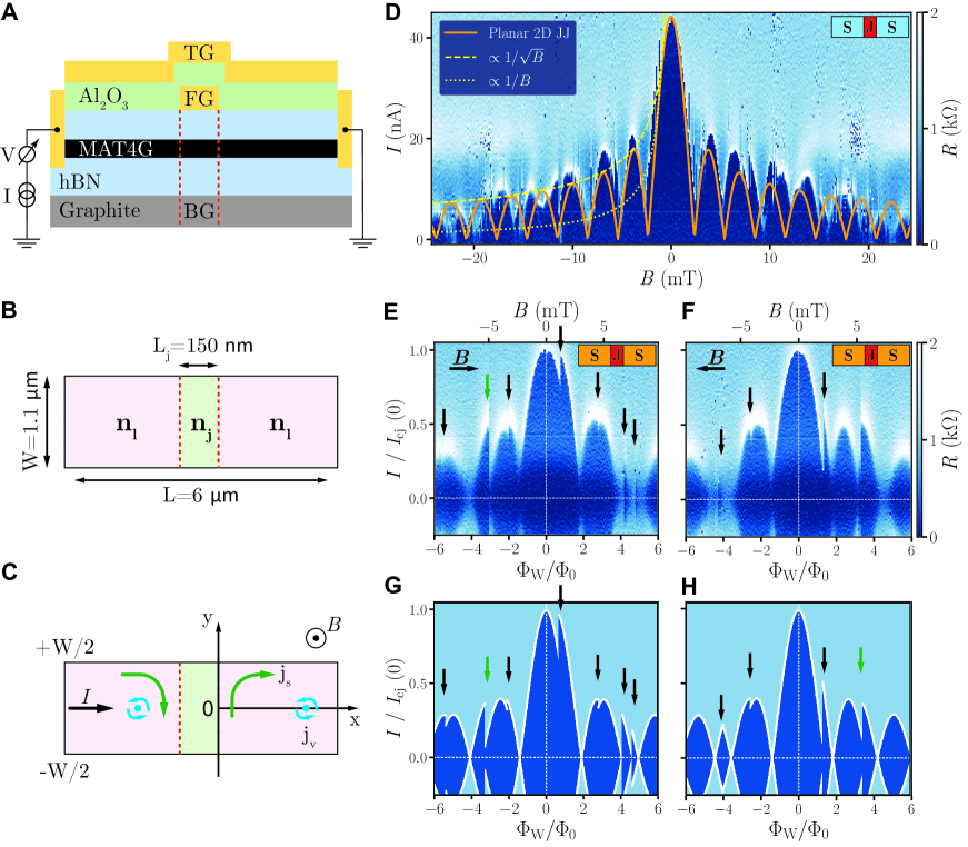
Here, we implement a gate-defined Josephson junction (JJ) in four-layer twisted graphene (MAT4G). Exposing the junction to a perpendicular magnetic field , we observe a distinct Fraunhofer-like pattern in the junction critical current . The interference pattern, see Fig. 1D, differs markedly from the one observed in standard junctions (?), a consequence of the extremely weak transverse magnetic screening power of these ultrathin films: i) The periodicity of the pattern is given by the flux with the junction width, a factor larger than the characteristic flux in usual junctions, where denotes the London penetration depth (?). And ii), the maxima in the Fraunhofer-like pattern decay slowly , rather than the usual decay ; recognizing these differences, in the following, we refer to our experimentally observed interference pattern as a Fraunhofer pattern (FP). Interestingly, our Fraunhofer pattern exhibits pronounced jumps, see Fig. 1, E and F, that we attribute to vortices jumping into and out of the superconducting leads. Our Josephson junction then serves as a sensor allowing for an indirect detection of vortices in gated atomically thin materials, circumventing the obstacles of traditional vortex imaging techniques (?, ?, ?, ?). Furthermore, we profit from the well developed phenomenology for these ultrathin materials (?, ?, ?, ?, ?, ?) that provides us with a strong basis for the quantitative analysis of our experiments, independent of the microscopic origin of superconductivity in this correlated material that is still under debate.
Setup
We have engineered a gate-defined JJ in a MAT4G film of width , length , and thickness (?). The device depicted in Fig. 1A features an alternating twist angle of and is tuned with three gates. A graphite bottom gate (BG) and a gold top gate (TG) are used to control independently the density and the displacement field in the leads. A junction of width and length is defined using a gold finger gate (FG), as shown in Figs. 1, A and B. The density and displacement field in the junction are tuned using both FG and BG. Three gates are used to tune the four parameters , , , and , implying that one parameter out of four cannot be independently controlled. All experiments are carried out at unless stated otherwise. The formation of a JJ is confirmed by the observation of the d.c. Josephson effect shown in Fig. 2C, as well as by magnetic interference measurements, with the resulting Fraunhofer pattern shown in Fig. 1D. Further details of the device fabrication and gate control are presented in the Supplementary Text (see figs. S1 and S2). Given the nanometer scale thickness of the film , the device belongs to the class of weak transverse screeners, with the effective screening power given by the Pearl length (?). With the width , external magnetic fields penetrate the entire sample and .
Bulk superconductivity
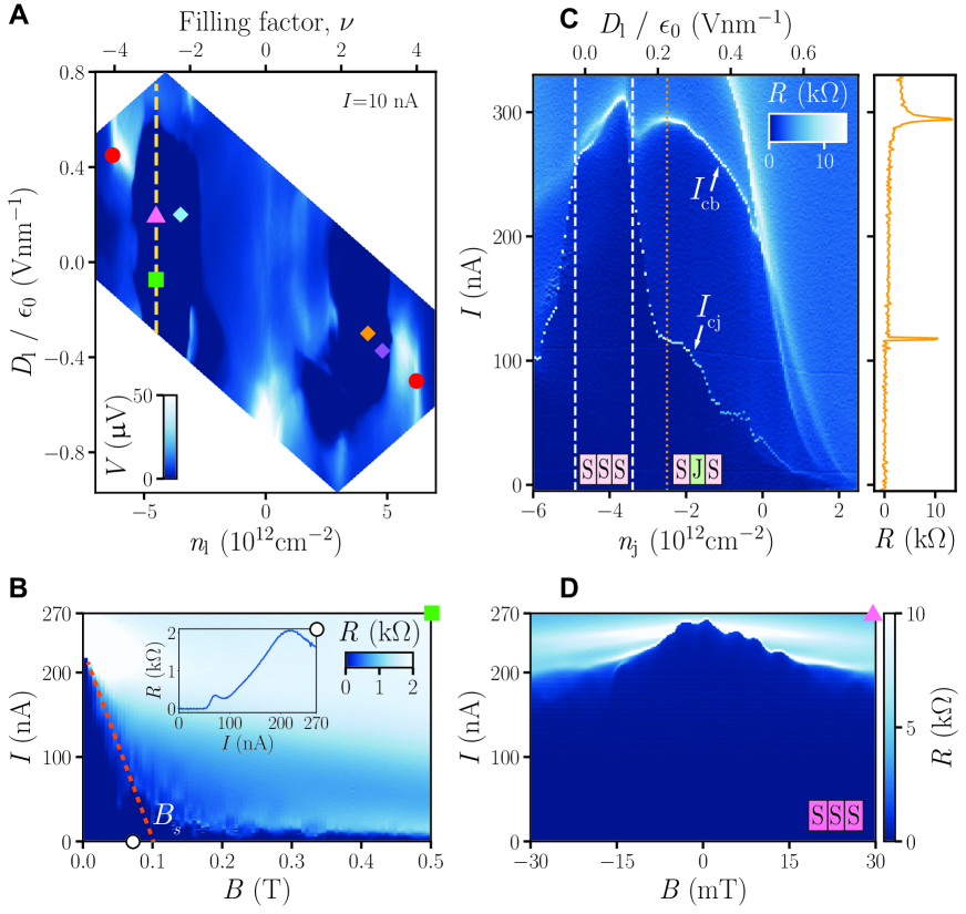
We first analyse the bulk superconductivity observed in our MAT4G device. In Fig. 2A the voltage measured at constant probe current in a 4-terminal configuration not crossing the junction is shown as a function of and (see Supplementary Text fig. S3B for the same measurement taken across the junction). Superconductivity is observed at moiré filling factors between (hole carriers with up to , see fig. S3C) as well as ( up to ), with at full filling, see also Supplementary Text. Strong out-of-plane displacement fields ( denotes the vacuum permittivity) quench the superconducting state due to the hybridization of the flat bands with the dispersive bands (?, ?, ?, ?). The bulk critical current is measured to be larger than in the superconducting regime for holes and larger than for electrons (see figs. S3, D and E). Further characterization of the superconducting domes is discussed in the Supplementary Text.
The dependence of the bulk critical current on the magnetic field applied normal to the sample plane is shown in Fig. 2B for the device tuned at the green square depicted in Fig. 2A. The critical current is seen as a peak in the differential resistance which is evaluated numerically from d.c. data (transition between dark blue in Fig. 2B, zero resistance, to a finite one, light blue), where the device switches to the resistive state due to vortex motion, see inset in Fig. 2B. The field dependence is governed by surface- and bulk pinning of vortices (?, ?, ?, ?, ?). The linear drop in at small fields is characteristic of the surface barrier preventing vortices from entering the sample (?, ?, ?), as is typical for such films. By linearly fitting the critical current versus magnetic field , we extract a value for the surface penetration field , see orange dashed line in Fig. 2B. Combining this result with the zero-field critical current and using the relation derived in Ref. (?), we arrive at an estimate for the London penetration depth of order , that compares favorably with values of a few m obtained from other estimates (here, is the vacuum permeability). For example, we may use the bulk critical current measured in Fig. 2B, obtain the critical current density , and take this value as a lower bound for the depairing current density (with denoting the flux unit). Extracting a value for the coherence length (?, ?, ?) from the measured critical field as a function of temperature (see fig. S4 in the Supplementary Text), we then find an estimate . Finally, the low value in the saturation of the critical current at large fields, see Fig. 2B, is testimony of weak bulk pinning (?).
Implementing the JJ
Keeping the leads in one of the superconducting regimes, we form a JJ in our sample by tuning the junction region into a resistive state. The high tunability of our device allows us to define a JJ in several ways by exploring the parameter space of density and displacement field in the leads and the junction (see Fig. 2A). In Fig. 2C, we illustrate the formation of a JJ with a reduced critical current by tuning the junction density at fixed and (the displacement field is slaved to and follows the yellow dashed line within the superconducting dome in Fig. 2A). The differential resistance then exhibits two steps, i) at low currents when the junction turns resistive, and ii) at high currents when the leads switch to the resistive state, see orange line-trace in Fig. 2C. The two critical currents coalesce when the junction density enters the superconducting state between the white dashed lines in Fig. 2C, resulting in a uniform superconducting device SSS. Thus, tuning the junction away from this region, we can implement a JJ with a desired critical current —we refer to this weak-link configuration as SJS, with J denoting the resistive junction region, notwithstanding its nature, metallic, semiconducting, or insulating. We note that our MAT4G device admits as an additional tuning knob for changing as compared to junctions defined in MATBG (?, ?) (see fig. S5F).
Regarding the issue of reproducibility in the formation of the JJ, we have performed multiple measurements of as a function of as well as magnetic field (see figs. S6, S7, and S12). We find that a reproducible JJ is only formed when is tuned to the full-filling peaks () as indicated by the red dots in Fig. 2A. When is tuned to any correlated insulator state, the measurements are not reproducible in time. Such reproducibility is an important feature in all practical use-cases of superconducting electronics.
Junction in magnetic field
A typical magnetic interference measurement with the device tuned to the junction regime is presented in Fig. 1D. The current is swept from negative to positive values while measuring the voltage drop across the junction, all at a fixed magnetic field . After each current sweep, the magnetic field is stepped and a new trace is recorded. The leads are set to the superconducting state (, , see the light blue rhombus in Fig. 2A) and the junction is gated to full filling (, , see the red dot in Fig. 2A); we call this the BRB (for blue-red-blue) setting with a corresponding identifier in the top-right corner of Fig. 1D. Note that a SJS device is characterized by a pair of points in Fig. 2A specifying density and displacement fields in the junction and the leads. By applying a perpendicular field , the critical current of the junction is suppressed and modulated, resulting in the Fraunhofer interference pattern shown in Fig. 1D—the observed pattern is typical for a short junction (?) and exhibits the hallmarks of a weak screening device (?, ?). We observe field-induced oscillations of the critical current with the interference period . The magnetic interference measurements are symmetric in current and do not show any skewness. Thanks to the high tunability of our device, we can study these interference patterns throughout the phase space of both junction and leads (see Supplementary Text for further measurements with different parameters and ).
To further prove that the measured interference pattern is due to the JJ rather than sample inhomogeneity, we carry out the same measurement with the JJ tuned into the superconducting lobe (SSS) as shown in Fig. 2D (with and , see the pink triangle in Fig. 2A). In this measurement, the critical current agrees with the one measured for the bulk up to small oscillations in at low fields; their periodicity closely matches the one observed in the pattern of Fig. 1D and we attribute them to a slight mismatch in the tuning between the leads and the junction regions. No interference pattern is observed when the device is fully superconducting, compare Fig. 1D with Fig. 2D.
Fraunhofer interference pattern
For a JJ under weak screening conditions with (?, ?, ?, ?) the critical current shows a non-standard Fraunhofer pattern . In a conventional Josephson junction, the magnetic field in the leads is screened on the distance , the bulk London penetration depth (?). As a consequence, the gauge-invariant phase difference across the junction involves the flux . However, when screening is weak, the field penetrates the leads completely and the corresponding result (?, ?)
| (1) |
deviates from the standard expression. First, the relevant flux associated with the junction is now given by the junction width only, , provided that the film leads are longer than the film width, , which is the case in our device. As a consequence, the oscillations in the Fraunhofer pattern appear on the scale rather than the usual periodicity . Hence the field-to-flux conversion involves only the width .
Second, the usual linear shape is replaced by a sine-function, . This is again due to the deep penetration of the field into the film, on the scale rather than : in thick superconductors, screening currents flow on the London scale and turn around sharply in the device corners on this small length scale. In atomically thin films, however, screening is weak and the currents bend smoothly around corners on the scale of the sample, see Fig. 1C. As a result, the component of the screening current density flowing along the junction edge vanishes on the scale when approaching the junction edges at , see Fig. 2 in Ref. (?). With the phase difference across the junction given by the relation (?) , one finds that flattens at the junction edges, which explains the factor in (1). This seemingly minor correction has profound consequences for the Fraunhofer pattern at large fields , producing a slow decay of the maxima in the pattern instead of the standard behaviour.
To relate these insights to our experiment, we find the junction critical current by integration over the junction dimensions: assuming a sinusoidal current–phase relation with a free shift parameter, the integral over can be evaluated exactly (?, ?) in terms of the Bessel function ,
| (2) |
where the choice produces the largest, hence critical, current. The Bessel function then replaces the -function characterizing the Fraunhofer pattern in the standard context (?). The orange line in Fig. 1D is a fit to the data that makes use of the width of the film in the determination of the flux . Given that the distance between consecutive zeros of the Bessel function is , we recover the periodicity . Note that the zeros in become truly equidistant only at large values of the magnetic field. Furthermore, the maxima are well tracked by the slow decay , see the dashed yellow line at .
The measured interference patterns fit with the theoretical prediction of Eq. (2) both when the JJ is tuned to full filling for electrons ( and ) and full filling for holes ( and ), see red dots in Fig. 2A. Our excellent fit of the Fraunhofer pattern goes beyond the results of similar experiments (?, ?, ?). The good agreement between the theoretical prediction and the experimental data holds at fields below , i.e., including the first three minima; thereafter, the fit does not work anymore due to the presence of sharp shifts in the pattern of the size of a fraction of . We attribute these shifts to vortices jumping into and out of the leads, as further discussed below.
Jumps in the Fraunhofer pattern
The measured interference patterns show sudden shifts, i.e., jumps in , see Figs. 1, D–F. The measurement protocol for the Fraunhofer pattern described above produces interference maps over time scales of hours. The sudden shifts appear in all of our junction tunings, i.e., independent of gate voltages, see fig. S11.
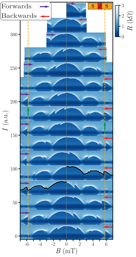
Pronounced jumps in , see black arrows in Figs. 1, E and F, are observed in an electron-doped state (with , and , , see the orange rhombus and red dot in Fig. 2A, we name it the orange-red-orange or ORO setting). They are present in both increasing and decreasing sweeps of the magnetic field, are symmetric in the current, and are stable over typical time intervals of order seconds, see fig. S14. Some jumps are found to be very reproducible as they tend to occur at similar values of the magnetic field, see the ones highlighted by the green arrows in Figs. 1, E and F at and the discussion of Fig. 3 below.
To further study these shifts, we measure in a consecutive manner, alternating the direction of the magnetic field-sweep in-between measurements and increasing the magnetic field range after each reversal, see Fig. 3 and fig. S13 (we use the same ORO tuning as for Figs. 1, E and F). The results exhibit some degree of hysteresis, as the central peak (see grey dashed line) of the interference pattern is shifted between sweeps. Reproducible jumps are observed, see orange dashed lines at , the jumps marked by green arrows coincide with the events observed in Figs. 1, E and F. Furthermore, the results tend to be symmetric for decreasing/increasing magnetic fields, see black traces in Fig. 3 measured for a decreasing field magnitude (see fig. S9 for the extraction method of these traces). The range of magnetic-field sweeps influences the appearance of shifts, with the first few curves in Fig. 3 at small sweep-range exhibiting almost no jumps.
Vortex jumps
With these shifts present in all of our device configurations, we rule out a possible origin related to the experimental setup (see Supplementary Text and fig. S10). We rather attribute these sudden shifts to vortices jumping in and out of the superconducting leads in the vicinity (closer than ) of the junction (?). Similar observations have been reported in the past: the influence of vortices on the FP of cross-strip Josephson junctions has been discussed for Pb-Bi films in Refs. (?, ?) and pronounced steps similar to those reported here have been observed in step-edge junctions of a cuprate superconductor (?). The deliberate placing of a vortex near a Josephson junction has been studied in Ref. (?), with the underlying theory developed later by Kogan and Mints (?, ?).
The presence of a vortex (at the position and with a flux parallel to the field) changes the phase pattern at the junction, , adding a step-like contribution , see figs. S15–S17 in the Supplementary Text. The phase as a function of (see Supplementary Text for an explicit expression) smoothens and decreases in amplitude with increasing distance of the vortex from the junction. Since the vortex currents (, blue in Fig. 1C) flow opposite to the screening currents (, green in Fig. 1C), the presence of a vortex decreases the effect of the field and the Fraunhofer pattern shifts to the right upon vortex entry at positive fields (the shift is to the left for a vortex with opposite circularity entering at ). This is exactly what is seen in the experiment. For example, in Figs. 1, G and H, we fit the experimental traces of Figs. 1, E and F by having 7 (in Fig. 1G) and 4 (in Fig. 1H) vortices of polarity enter (upon increasing ) or leave (upon decreasing ) the device, see black and green arrows. In our fit, we place the vortices in the film center, i.e., , and tune the pattern’s shifts by choosing vortex positions in the range , see Fig. 1C (detailed parameters are given in the Supplementary Text). Note that in Figs. 1, E and F, vortices have left the device at zero field in both cases. This is different in Fig. 3 where the central peak appears shifted in some of the traces due to the presence of vortices remaining at vanishing field. Pushing the field amplitude too far up, beyond , the patterns turn blurred and the observation of individual jumps gets hampered.
A further test of our interpretation of pattern-shifts due to vortex jumps is provided by the minimal field for metastable vortex configurations, see Ref. (?) and the Supplementary Text. Using the results in Ref. (?), we find the first (meta-)stable position inside the film appearing at , i.e., within the main dome () of the Fraunhofer pattern. Typical barriers the vortices have to overcome are of order (?) , see fig. S18A in the Supplementary Text, where is the vortex line energy. On the other hand, analyzing the time traces of fluctuating currents, we can derive an energy scale for the typical barriers for vortex entry: given a barrier at temperature and an attempt time , a vortex requires a time to overcome the barrier (we set to unity). Knowing the typical dynamical time for shifts in the Fraunhofer pattern, we can derive a quite accurate estimate for the barrier (we choose , an attempt time (?, ?) , and a typical dwell time as observed in our experiments, see fig. S14). Equating the two, , we extract for the London length. These results are in good accord with the recent determination of the superfluid stiffness via kinetic inductance measurements in twisted films, see Refs. (?, ?). Indeed, the reported (?) value around optimal gating is quite consistent with our estimate for the fluctuation barrier (where the factor accounts for the difference in film thicknesses).
Vortex fluctuations
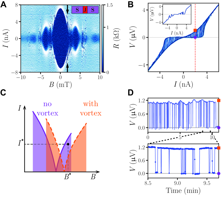
We close our discussion with the analysis of another data set with the leads tuned to the edge of the superconducting region, see purple rhombus and red dot in Fig. 2A (, and , ). This choice of parameters leads to a reduction in the superfluid stiffness in the lead, see Ref. (?). The Fraunhofer pattern in Fig. 4A exhibits pronounced bi-stability effects in . These derive from rapid switchings between superconducting (purple circle) and dissipative (orange square) states in the – traces as shown in Fig. 4B and its inset (recorded at , black arrows in Fig. 4A). The timescale of these fluctuations is on the order of seconds, see the time-dependent measurement in Fig. 4D taken at (red dashed line in Fig. 4B). The counting statistics of these fluctuations is analyzed in the Supplementary Text, see fig. S8.
We attribute these rapid switchings between states to vortex fluctuations. As seen before, a vortex jumping into and out of the leads produces shifts in the Fraunhofer pattern. Fixing the field and the bias current at a point where the presence (absence) of a vortex causes to be lower (higher) than the bias current , see Fig. 4C, produces the observed jumps in voltage traces which we correlate with jumps of vortices. The reduced superconducting stiffness results in a smaller barrier for thermal vortex dynamics and thus a shorter dwell time between jumps. Indeed, the typical dwell time in Fig. 4D is of order and following the argument presented above, we find that , about 3/4 of the value found previously.
Conclusion
In conclusion, we have demonstrated the formation of a gate-defined Josephson junction in MAT4G and its application as a vortex sensor. The measured interference patterns agree excellently with the predicted behaviour for a weak transverse screener with a Pearl length surpassing the sample dimension, . Our data enable us to precisely track the entry and exit of vortices. By fitting the data, we can accurately position the vortices within the leads. Observing vortices in MAT4G opens new avenues for exploring vortex motion in this new class of twisted materials. Gaining deeper insights into their dynamics offers a significant advance in the engineering of thin-film superconducting devices.
References
- 1. Y. Cao, et al., Nature 556, 80 (2018).
- 2. M. Yankowitz, et al., Science 363, 1059 (2019).
- 3. X. Lu, et al., Nature 574, 653 (2019).
- 4. Y. Cao, et al., Nature 556, 43 (2018).
- 5. J. M. Park, Cao, et al., Nature 590, 249 (2021).
- 6. Z. Hao, et al., Science 371, 1133 (2021).
- 7. S. Carr, et al., Physical Review B 95, 075420 (2017).
- 8. J. M. Park, et al., Nature Materials 21, 877 (2022).
- 9. D. Rodan-Legrain, et al., Nature Nanotechnology 16, 769 (2021).
- 10. F. K. de Vries, et al., Nature Nanotechnology 16, 760 (2021).
- 11. J. Díez-Mérida, et al., Nature Communications 14, 2396 (2023).
- 12. E. Portolés, et al., Nature Nanotechnology 17, 1159 (2022).
- 13. H. Kim, et al., Nature 606, 494 (2022).
- 14. Y. Zhang, et al., Science 377, 1538 (2022).
- 15. G. W. Burg, et al., Nature Materials 21, 884 (2022).
- 16. E. Khalaf, et al., Physical Review B 100, 085109 (2019).
- 17. M. Tinkham, Introduction to Superconductivity, Dover Books on Physics Series (Dover Publications, 2004).
- 18. U. Essmann, H. Träuble, Physics Letters A 24, 526 (1967).
- 19. H. Hess, et al., Physical review letters 62, 214 (1989).
- 20. J. Bending, Advances in Physics 48, 449 (1999).
- 21. L. Embon, et al., Scientific Reports 5, 7598 (2015).
- 22. G. Stejic, et al., Phys. Rev. B 49, 1274 (1994).
- 23. M. Moshe, V. Kogan, others., Physical Review B 78, 020510 (2008).
- 24. J. R. Clem, Physical Review B 81, 144515 (2010).
- 25. V. Kogan, R. Mints, Physical Review B 89, 014516 (2014).
- 26. V. Kogan, R. Mints, Physica C 502, 58 (2014).
- 27. F. Gaggioli, et al., Phys. Rev. Research 6, 023190 (2024).
- 28. P. Rickhaus, et al., Science advances 6, eaay8409 (2020).
- 29. J. Pearl, Applied Physics Letters 5, 65 (1964).
- 30. C. P. Bean, J. D. Livingston, Physical Review Letters 12, 14 (1964).
- 31. A. Larkin, Y. N. Ovchinnikov, Journal of Low Temperature Physics 34, 409 (1979).
- 32. G. M. Maksimova, Fiz. Tverd. Tela (St. Petersburg) 40, 1773 (1998). [Physics of the Solid State 40, 1607 (1998)].
- 33. B. Plourde, et al., Physical Review B 64, 014503 (2001).
- 34. A. Barone, G. Paterno, et al., Physics and applications of the Josephson effect (John Wiley, 1982).
- 35. P. Rosenthal, et al., Appl. Phys. Lett. 59, 3482 (1991).
- 36. R. Humphreys, J. Edwards, Physca C 210, 42 (1993).
- 37. O. Hyun, et al., Phys. Rev. Lett. 58, 599 (1987).
- 38. O. Hyun, et al., Phys. Rev. B 40, 175 (1989).
- 39. E. Mitchell, et al., Physica C 321, 219 (1999).
- 40. T. Golod, et al., Physical review letters 104, 227003 (2010).
- 41. A. P. Malozemoff, M. P. A. Fisher, Phys. Rev. B 42, 6784 (1990).
- 42. V. Kopylov, et al., Physica C 170, 291 (1990).
- 43. A. Banerjee, et al., Superfluid stiffness of twisted multilayer graphene superconductors (2024).
- 44. M. Tanaka, et al., Kinetic inductance, quantum geometry, and superconductivity in magic-angle twisted bilayer graphene (2024).
Acknowledgments
We thank Peter Märki and the staff of the ETH cleanroom facility FIRST for technical support. We acknowledge fruitful discussions with Vladimir Kogan and Manfred Sigrist. We thank Giulia Zheng for her support during the project. Financial support was provided by the European Graphene Flagship Core3 Project, H2020 European Research Council (ERC) Synergy Grant under Grant Agreement 951541, the European Union’s Horizon 2020 research and innovation program under grant agreement number 862660/QUANTUM E LEAPS, the European Innovation Council under grant agreement number 101046231/FantastiCOF, the EU Cost Action CA21144 (SUPERQUMAP), and NCCR QSIT (Swiss National Science Foundation, grant number 51NF40-185902). K.W. and T.T. acknowledge support from the JSPS KAKENHI (Grant Numbers 21H05233 and 23H02052) and the World Premier International Research Center Initiative (WPI), MEXT, Japan. F.G. is grateful for the financial support from the Swiss National Science Foundation (Postdoc.Mobility Grant No. 222230).
Author contributions:
M.P. fabricated the device. T.T. and K.W. supplied the hBN crystals. M.P. and C.G.A. performed the measurements. M.P. and C.G.A. analyzed the data. F.G., V.G. and G.B. developed the theoretical model. M.P. and G.B. wrote the manuscript, and all authors were involved in the reviewing process. M.P., E.P., K.E. and T.I. conceived and designed the experiment. T.I. and K.E. supervised the work.
Competing interests:
The authors have no competing interests.
Data and materials availability:
The data that support the findings of this study will be made available online through the ETH Research Collection.