A 9T4R RRAM-Based ACAM for Analogue Template Matching at the Edge
Abstract
The continuous shift of computational bottlenecks to the memory access and data transfer, especially for AI applications, poses the urgent needs of re-engineering the computer architecture fundamentals. Many edge computing applications, like wearable and implantable medical devices, introduce increasingly more challenges to conventional computing systems due to the strict requirements of area and power at the edge. Emerging technologies, like Resistive RAM (RRAM), have shown a promising momentum in developing neuro-inspired analogue computing paradigms capable of achieving high classification capabilities alongside high energy efficiency. In this work, we present a novel RRAM-based Analogue Content Addressable Memory (ACAM) for on-line analogue template matching applications. This ACAM-based template matching architecture aims to achieve energy-efficient classification where low energy is of utmost importance. We are showcasing a highly tuneable novel RRAM-based ACAM pixel implemented using a commercial 180nm CMOS technology and in-house RRAM technology and exhibiting low energy dissipation of approximately 0.036pJ and 0.16pJ for mismatch and match, respectively, at 66MHz with 3V voltage supply. A proof-of-concept system-level implementation based on this novel pixel design is also implemented in 180nm.
I Introduction
IN recent years, the main driving technology of electronic circuits and systems, the MOSFET technology, is showcasing important difficulties in keeping up with the increasingly higher computing demands through scaling [1]. Simultaneously,it has been shown that one of the most inhibiting factors in modern systems’ performance is the data movement that occurs in modern highly distributed edge computing networks, where a large amount of interconnected sensors, edge computers and servers are constantly communicating transferring huge amounts of data [2, 3, 4].
Recently, a lot of focus has been given to novel wearable and implantable edge devices aimed at sensing specific bio-signals and transferring information about health and activity [5, 6, 7]. Brain Machine Interface (BMI) devices are one of these novel edge computing applications for monitoring brain activity [8], a process that can be helpful in advanced medicine, such as better understanding and treating brain-based diseases as well advancing the frontier of neural prosthetic development [9]. A cornerstone operation that enables BMI implementations is real-time template matching, where an analogue signal can be quickly compared against a set of predefined templates and potentially identified as one of them. This enables a fast and low power classification operation near the signal’s origin.
Template matching approaches enables the implementation of novel low-power pattern recognition engines capable of being closely integrated with edge sensors. Content Addressable Memory (CAM) is the main system employed for many template matching applications [10, 11, 12, 13, 14]. CAMs are memory-centric systems that are deploying large memory arrays with hardware-level optimisation that enable fast parallel search and match capabilities. Their template match operations are based on a query input that is compared (in a massively parallel manner) with all stored templates of the CAM array [15]. The general architecture of CAMs is based on the implementation of memory arrays with each cell of the array being modified to perform an in-situ comparison between an input signal and the contents of the memory cell with each row being organised as a template [16, 17]. By providing an input query vector, we are able to perform a parallel comparison of this input with every template. The sensing front-end circuitry of an edge application usually deals with analogue stimulus from its environment, therefore consuming high energy and latency penalty for analogue-to-digital conversion (ADC). Analogue CAMs (ACAMs) [15] can play an important role in eliminating the analogue/digital cross-interfacing penalty, where analogue inputs can be classified on-the-fly without converting them into the digital domain. This reduces not only the design complexity but also the data-transfer bandwidth, enabling the implementation of novel energy efficient always-on classification engines at the edge.
At the same time, advances in emerging memory technologies introduce a new component for novel analogue circuit design. Memristors, also known as Resistive Random Access Memory (RRAM), are two-terminal, tuneable, non-volatile, nanoscale resistive memory devices [18, 19]. RRAM has many beneficial traits over conventional memory devices [20, 21, 22]. RRAM can be integrated to implement novel computing systems showcasing low power consumption, high throughput, low area of integration and multi-bit information stored per cell compared to their fully CMOS counterparts [21, 23]. Thus, RRAM is considered as an excellent candidate for building ACAMs. Each RRAM device is capable of storing multi-bit information per single device in the form of resistance [24]. The different resistance values form the analogue matching windows of each ACAM cell [25].
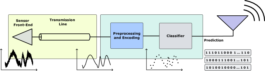
Fig. 1 shows the concept of the proposed system where the ACAM-based template matching approach is used to perform classification on the edge, tightly coupled with the sensing front-end. In this case, the ACAM implements the classifier as shown in Fig. 1. The dataflow of showcased paradigm includes capturing analogue signals through a specialised sensor, preprocessing this stimulus and then providing it in form of queries to the template matching classifier. The front-end circuitry detects and amplifies the bio-signals and then forwards them to the near-sensor RRAM-based ACAM edge classifier. The detected signals will be sampled and compared to the pre-trained templates to reach a classification decision. Based on the templates stored in ACAM, a match window per cell can be defined with the query value connected to each cell being compared with this memory-defined window. Different matching conditions can be implemented when assessing the results of ACAM through exact match, best match and threshold match. For different matching instructions a different matching comparator network needs to be implemented (e.g., a Winner-Take-All Network for best match) Depending on the applied matching policy followed by the implementation, different outputs can result from the classifier. In general, the more inputs of the query vector falls within the matching windows of the template’s cells, the higher the matching level of the query with the specific template.
In this work, we are showcasing a novel RRAM-based analogue Template matching piXeL (TXL) used to implement an energy efficient ACAM system (TXL-ACAM) towards accelerating analogue near-sensor template matching operations at the edge. We are showcasing a hybrid CMOS-RRAM IC using 180nm CMOS technology and in-house RRAM technology integrated as back-end-of-line (BEOL). The implemented array of the prototype TXL-ACAM is array. The TXL-ACAM integrates a array, with 2K RRAM devices, and a polysilicon-based emulator array. The area of integration for the prototype TXL-ACAM is approximately . The 9T4R TXL design is using 2 RRAM reconfigurable devices while the other 2 resistive elements are implemented as conventional polysilicon devices. The cell design can exhibit competitive energy dissipation of approximately in worst case scenario (matching cell for input close to the operating voltage of 3V). Peripheral circuit is also implemented enabling the programming and readout of the RRAM-based ACAM array. The proposed TXL-ACAM energy efficient inference engines can reduce the data transfer between sensors and higher performance systems by classifying information at the edge.
The rest of the paper is organised as follows: In Section II, we present the main background of the RRAM-based analogue and digital CAMs. In Section III, we showcase the proposed TXL ACAM cell design and operation, and its performance as well as comparison with state-of-art. In Section IV, we exhibit the hardware implementation of a TXL-based ACAM array alongside the necessary peripherals. Finally, in Section V, we discuss our findings and conclusions.
II Background
In the last decade, many different RRAM-based circuits and systems have been proposed that introduce information processing at the analogue domain. RRAM is mainly aimed at memory-centric applications where RRAM’s key capabilities, such as storing multiple bits of information per devices and being non-volatile, enable the development of novel electronics that can better emulate neuro-inspired operations. One such neuro-inspired in-memory computing application is Associative Memory and its main digital emulation the CAMs [26]. Although digital or ternary CAMs have seen a lot of development, analogue CAMs’ (ACAMs) development, which can be used as a better analogue to the associative memory recall systems observed in biological neural networks, was inhibited by the lack of a appropriate analogue nanoscale device. The integration of RRAM devices into CAMs has re-invigorated the design of neuro-inspired associative recall functions through the development of novel ACAMs [27]. ACAMs can be leveraged to perform complex look-up operations through large sets of stored templates. Additionally, they can calculate the similarity of an input with each one of these templates through approximate computing techniques in the analogue domain [27, 28]. The use of RRAM-based circuits capable of storing and processing multi-bit information enabled the close integration of such systems with the sensors and pre-processing analogue circuits, that capture the stimulus from the environment, since no conversion to binary is required. Thus, processing the information without the need to transfer them into the digital domain is possible, minimising a process known for being costly in terms of IC area, power and delay.
There is a variety of different pixel designs for implementing hybrid RRAM-CMOS CAM systems. Compared to the conventional fully CMOS CAM cells, usually configured as SRAM-based circuits [29], RRAM-CMOS cells showcase better power efficiency, lower area of integration, non-volatility and capability in storing multi-bit information [30, 14, 15]. Towards providing novel solutions for enhancing CAM and ACAM systems, many different hybrid CAM cell designs using emerging memory technologies have been proposed in recent years. In [31], a 6T2R ACAM cell is presented that uses two 1T1R voltage divider circuits to map the lower and upper thresholds (that determines the matching window of the cell). Additionally, another four transistors implementing a CMOS inverter to enable complementarity of the upper threshold control in defining the matching window of the cell and two nMOS transistors for the per cell comparison are also used for a total of 6T2R design. The design exhibits good performance and tuneability with each two bounds mapped as resistance states in the two RRAM devices used. ACAM cells such as the one exhibited in [31] use resistive voltage dividers (through 1T1R) to read the memory and perform the per cell match operation. The use of 1T1R in general results in smaller pixel size and thus increases array density but introduces static power consumption during ACAM search operation, since it requires to apply a reference readout voltage to the two 1T1R branches. The per cell comparison uses the intermediate voltages of the two 1T1Rs which are creating a direct resistive path between the reference readout voltage and ground. Techniques to minimise the static power dissipation by applying a small reference readout voltage or by using large resistive states for RRAM could be applied but might not be possible for different RRAM technologies. Additionally, by using CMOS design to map the cell threshold, instead of the conventional 1T1R branches, we could eliminate the static power during the search operation while retaining the capability of programming arbitrarily matching windows per cell. Saving static power through hybrid RRAM-CMOS logic could provide an interesting trade-off between power and pixel size that depending on the application could be worth considering.
In [32], a 1T1R+2T pixel design for ACAM is showcased as a novel form of less complex ACAM cell requiring half the area compared to the current state-of-art 6T2R ACAM cell design [14]. The 1T1R+2T cell is one of the compact designs for ACAM systems comprised of only 3 transistor devices and one RRAM device acting as the memory element. Although the area and energy of the 1T1R+2T shows promising results, it has some limitations in terms of tuneability of its low and high threshold. This is due to the design using only one RRAM device and 2 MOSFET devices to effectively trigger the thresholds based on the voltage threshold of the MOSFET technology employed. In [25], a 6T2R template matching cell is proposed for event generation when a specific voltage value is provided as stimulus. This design showcases good power consumption during template matching operation and exhibits competitive area usage but it has some limitations in terms of configurability of the matching window as well as with accessing the RRAM devices for programming, thus requiring some additional access circuit. Additionally, the cell’s response is dependent on a current mirror that increases the amplitude of the generated spike (used to logically map the event) which will require careful calibration and design to avoid having substantially different spike generation amplitudes in a large array.
III 9T4R Cell Design and Operation
The TXL circuit has the topology of two hybrid RRAM-CMOS 2T2R inverters and an additional CMOS-based output network controlled by the two 2T2R hybrid inverters. The input signal is connected to the input of the RRAM-CMOS inverters (gate nodes of the MOS components in a conventional CMOS inverter connectivity). The RRAM devices are placed between the pMOS and connection and between the nMOS and the GND node for the pull-up and pull-down network of the hybrid inverter, respectively. The output of one hybrid inverters controls the gate of the output pMOS device and the output of the other hybrid inverter controls the gate of the output nMOS device. Through this configuration, a comparison of the input with the stored matching window (determined by RRAM conductance states) is possible.
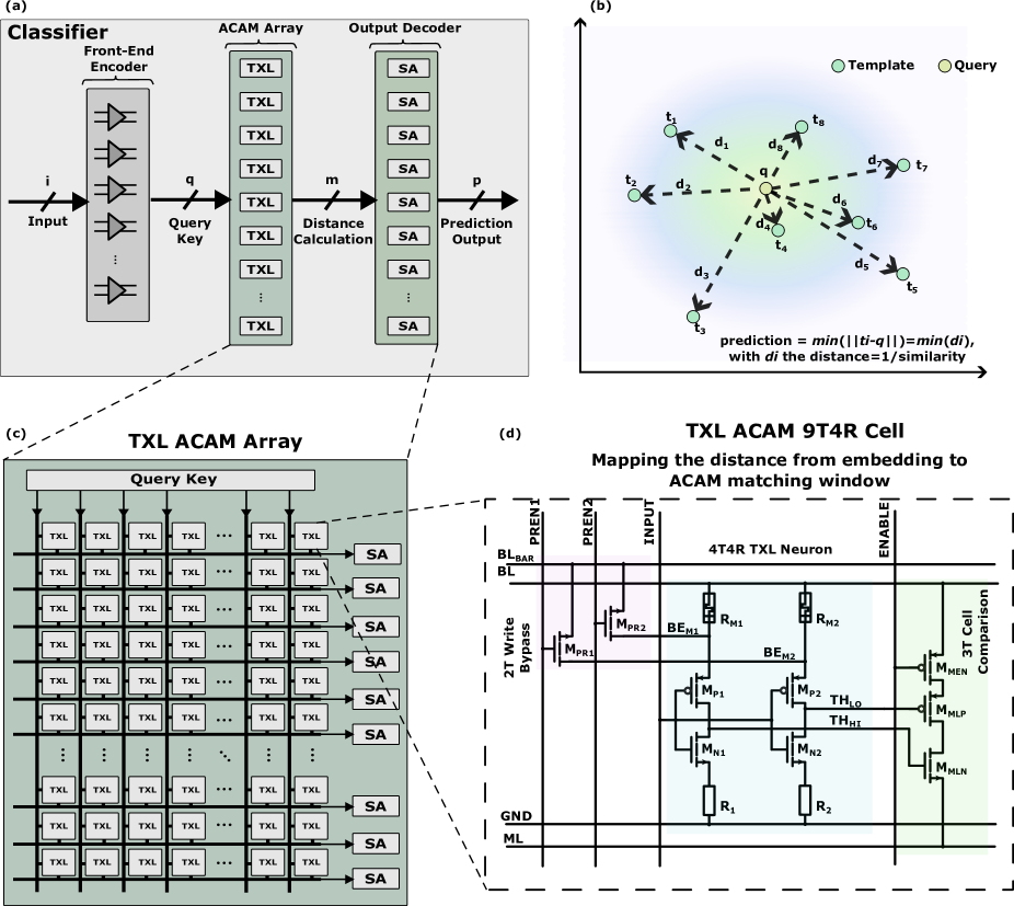
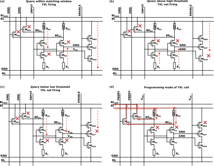
In Fig. 2(d), a schematic representation of the 9T4R ACAM pixel is shown. The memory part is based on the use of two hybrid RRAM-CMOS inverters (2T2R circuits) with each such hybrid inverter mapping one of the two thresholds/bounds. The threshold is effectively defined based on the ratio of the upper and lower RRAM device which shifts the voltage threshold of the hybrid inverter (thus the value of input voltage that the inverter changes output). The cell-wise comparison part is comprised of 3 MOSFET devices, one pMOS and one nMOS serially connected to multiply the low and high threshold memory read and one power-gating pMOS device that enables the charge of the matchline when the memory read operation is active and at the same time is performing a current limiting operation to appropriately adjust the charging rate of the matchline. This is performed by applying an appropriate biasing voltage () to partially open the power-gating pMOS of the cell’s comparator part. This per cell current limiter is useful for calibrating the cell charging capability depending on the size of the implemented array and/or the detection requirements of the accompanying sense amplifiers, thus it is an aspect of convenient configurability of the cell output.
To enable an appropriate path for programming the RRAM devices and , two additional MOSFET devices are used as access transistors during the programming/setup mode of the RRAM array where the RRAM devices are being set to the appropriate conductance states. If the cell is in programming mode, the path connecting the RRAM to the ACAM cell is being cutoff and the circuit uses these extra 2 nMOS devices to effectively operate the two RRAM as two 1T1R circuits. By accessing the RRAM devices between the and and bottom electrodes provides a direct low resistance path for programming the RRAM devices. This negatively affects the density of the proposed ACAM cell design since it increases the necessary area of the cell, but the included programming specific accompanying nMOS devices enable proper access to program the RRAM devices. In this specific configuration, only the upper resistive elements are assumed to be programmable RRAM devices, while the lower resistive elements take the form of conventional polysilicon-based resistors.
The circuit performs a pattern matching operation between its input signal and its stored patterns (stored in the form of programmable conductances through the integration of the nonvolatile RRAM devices). Each hybrid inverter stores one of the bounds by appropriately configured RRAM devices. By convention, we consider that the actual bound is stored into one of the two RRAM devices (per hybrid inverter) while the other is being set to an appropriate mean value (between the lowest and highest conductance value attainable by the RRAM devices) and used as a reference conductance that enables an appropriate ratio in the hybrid voltage divider (hybrid inverter). The use of two RRAM devices per bound enable a better dynamic range for expressing conductance thresholds in our design. The reference RRAM devices are meant to be programmed once with a periodic refresh of their state to eliminate any conductance drift. The threshold RRAM devices are meant to be programmed each time a new set of patterns need to be mapped into the TXL-CAM system.
After programming the RRAM-based conductances to appropriate values, the input signal (it could be either digital or analogue) is introduced to the input of the dual hybrid inverters mapping the two thresholds. The output of the hybrid inverters drives a custom pull-up network (consisting of pMOS and nMOS devices) which can detect the match of the input when sits between the lower and upper bound of the cell by connecting the high rail voltage (with being connected to ) to the matchline. In different case, we have a mismatch. The comparator part is power gated by a pMOS devices that is controlled by the global enable signal. The enable signal either cuts-off the power to the comparator part (during initialisation) or bias the power gating pMOS to a specific resistive state (during the evaluation phase). The biasing of the comparator branch effectively enforces a current limiting effect which results in a quick spike-like pulse of specific amplitude to appear in the matchline (for a given time of evaluation period). The charge limiting effect on the comparator branch has two effects. Firstly, it limits the power consumption per cell due to smaller voltage level transitions for the matchline. Secondly, it enables the analogue accumulation of charge in the matchline since we can define threshold above which the accumulated charge in the matchline triggers a match. The charge for each cell is accumulated using an analogue integrator circuit based on capacitor. If multiple cells have a match with the query input then multiple connection to are enabled and the match line is driven at some specific rate (dependent on the number of match enable available per TXL-CAM array) to high voltage. The output sense amplifier reads the matchline and can detect if we have an (overall) match of the query to a specific TXL-CAM word. The sense amplifiers are calibrated to detect a specific voltage level which is translated to match based on the time-to-charge of the matchline. In case no such voltage level is observed within the readout operation timeframe, then the template is considered to not match with the input query.

An important aspect of using a more complex design like the 9T4R against the state-of-the-art 6T2R is the use of hybrid RRAM-CMOS inverters as a method of reducing the dynamic power consumption of the template matching operation. The template matching operation in many RRAM-based cells usually involves the use of voltage dividers (i.e. through the use of 1-transistor-1-RRAM (1T1R) memory cells), thus creating a direct path between the high voltage node and the ground. By using RRAM-CMOS -based inverters (2T2R primitive circuit), we are effectively capable of performing a memory read operation and having only temporary dynamic power dissipation (pMOS and nMOS conductive at the same time). The "memory read" operation for the case of 2T2R hybrid inverter is encoded into the inverter’s threshold voltage, thus the input voltage point for which the inverter output is switching. Hence, not only we are reducing the power dissipation on the output part of the cell with smaller transitions of the matchline charging-discharging cycle, but also we are reducing the power dissipation of the ACAM cell during template matching operation. Although our proposed 9T4R cell requires more area per cell to implement arrays, in an assumed program-once-read-many application scheme (where the RRAM-based memory will be programmed once and then used for a long time before the next RRAM conductances update) the trade-off could be considered promising when we focus on the power consumption aspect of the ACAM for applications on the edge. Moreover, the use of RRAM-based ratio-based mapping of the analogue threshold values can enable the integration of a wider range of RRAM technologies, that showcase different ranges of viable resistive states and intrinsic behaviour, into the proposed 9T4R (compared to other ACAM pixel designs that base their memory read operation on voltage dividers) thus making the proposed design potentially more technology-agnostic.
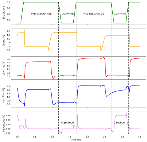
For the comparison of our proposed 9T4R cell design with the current state-of-the-art, both cell types were designed and simulated in the same commercially available 180nm technology and the same assumptions for the integrated RRAM technology were used towards adapting the MOSFET devices to the RRAM specifications (e.g. high current pass-through the accompanying MOSFET devices). The implementation employs 5V components of the 180nm library to enable the use of high electroforming voltage necessary for the RRAM technology under investigation. The precharge/enable signals period was set for = 15ns with = 5ns during assigned for memory read operation and = 10ns) for pre-charging/initialisation (see Fig. 2(b)). We are assuming that = 10ns of precharge are useful in case a large ACAM matchline needs to be precharged to . The memory part of both cells is power gated and is turned off during the matchline initialisation phase to minimise the power consumption.
| Energy | ACAM Pixel Designs | |||
|---|---|---|---|---|
| Figures | 6T2R [31] | TXL 9T4R | ||
| Input range | Low | High | Low | High |
| Match | 2.25pJ | 152fJ | 168fJ | |
| Mismatch | 479.2fJ | 3.84pJ | 30fJ | 130fJ |
As we can see from the figures in Table I, for both match and mismatch, the proposed 9T4R exhibits better power consumption over the evaluation period (which was set for one = 15ns period). More specifically, for the case of match, 9T4R consumes on average only = 0.16pJ while the 6T2R consumes 2.25pJ. Similarly for the case of mismatch, 9T4R consumes on average only = 0.08pJ while the 6T2R state-of-art consumes on average 2.1pJ (minimum energy approximately 0.479pJ and maximum energy approximately 3.84pJ). It is worth noting that especially since the memory read part is based on read operation on RRAM devices, the energy dissipation is strongly correlated with the memory state of the ACAM cell (the low and high bound mapped to RRAM states) and the input stimulus, that controls the voltage divider for the case of the 6T2R pixel and the hybrid inverter for the case of 9T4R (due to source degeneration of the MOSFET devices). Thus, it can be observed that a variability of energy dissipation exist based on the exact configuration of the cell’s RRAM conductance and the input stimulus it receives. To overcome this issue and provide an indicative approximate energy figure, we are calculating the energy dissipation during a clock cycle (for our testbench this is = 15nsec) and make this calculation for different configurations of the testbench. We are calculating an average (as shown in values of Table I) based on our calculations which is indicative of each cell’s performance. The matchline discharge/charge mechanism consumes approximately the same power between the different designs. The 6T2R consumes approximately 0J in case of a match while the opposite occurs for the 9T4R cell, which consumes approximately 0J in case of a mismatch. This is due to the event generation nature of the 9T4R comparison mechanism when we have a hit. The 9T4R cell’s response takes the form of a short pulse that is "fired" when a match occurs instead of keeping the matchline precharged only to be discharged for the case of a mismatch. Thus, although the 9T4R is larger in area than the 6T2R, it showcases advantages in terms of energy efficiency. This efficiency of the 9T4R cell design can be further enhanced in system-level applications especially for in-sensor or near-sensor approaches for bio-signal classification, an area that is known to have sparse event while requires always-on sensing and classification of the input stimulus [33].
IV ACAM System for Template Matching
In this section, we are showcasing a prototype IC design developed using the proposed 9T4R ACAM cell as its building block. The IC is designed using 5V components of the above-mentioned 180nm technology and uses a full analogue design flow for this fully custom ACAM macro cell. A 9T4R-based 32x48 ACAM array alongside the necessary peripherals to access the RRAM devices for programming and reading as well as for performing the parallel template search and match operation was integrated into a single silicon IC with all CMOS circuits being implemented as computing substrate and the RRAM devices are added with our in-house Back-End-Of-Line (BEOL) process. A block diagram of the prototype IC is shown in Fig. 6(a) while the physical layout of the implemented prototype IC is shown in Fig. 7(a) alongside some notes with regards to IC’s general floorplan.
Since the prototype IC is aimed at analogue template matching based on analogue information captured through a single input channel, a custom S&H circuit to sample incoming continuous input is implemented. This is widely used for near-sensor edge computing such as spike-sorting in BMI, bio-signal classification applications, etc. Thus, the assumption followed for this IC design is that the front-end sensing and pre-processing circuitry should be supplying a pre-processed analogue signal to our proposed IC design. The 9T4R-based ACAM IC is capable of classifying the pre-processed input signal without requiring any analogue-to-digital conversion but by performing the massively parallel search and match operation of ACAM in the analogue domain.

After the sampling operation is complete, analogue buffers are used to supply the input samples to the ACAM array as the input query, to be compared with the stored templates and identified. Due to the nature of the proposed ACAM design that generates a charge event per cell that has a match, a custom capacitor-based accumulator circuit for gathering the match event contributions is used per matchline. The accumulator is attached to the sense amplifier which is used to digitise the ACAM read operation and provide the output of the ACAM array by applying a threshold matching operation. Every matchline that exceeds a specified level of matching, which is based on the number of match events generated for each matchline, is considered to have a matching template to the input query. The threshold can be arbitrarily selected and provided to the sense amplifiers. The sense amplifier design is a voltage-mode dynamic latch comparator variant customised to sense the range of matchline voltage readout. The outputs of the sense amplifiers are connected to a custom Parallel In Serial Out (PISO) shift register which is loading all sense amplifier outputs in parallel and then serially shifting the outputs to a single pin. The PISO uses separate load and shift controls to easily configure the output readout operation.
Similarly, with regards to the necessary configuration digital signals used to control the ACAM IC, a custom Serial In Parallel Out (SIPO) shift register. For each operation, the SIPO is loaded serially with all necessary control bits and then the connection between the SIPO and the rest of the ACAM IC is enabled to configure a specific state of operation. The connection between the SIPO and the rest of the array is controlled by tri-state buffers that can be configured to leave the connection floating during the SIPO loading operation. Custom drivers to enable programming and characterisation of the RRAM devices, alongside the control logic, are also included to provide the nominal 3V supply to the array during the parallel search and match operation as well as programming voltages (up to 5V) when a standalone RRAM is accessed through the per cell access transistors. A block diagram of the TXL 9T4R-based ACAM IC is shown in Fig. 6(a), where many of the main circuits used for the peripherals are also shown. The schematic of the sample and hold circuit, the analogue drivers, the programming circuit and the sense amplifiers are all shown in Fig. 6(b),(c),(d),(e), respectively.

| Prototype IC | ACAM IC Designs | |
|---|---|---|
| Implementation | [31] | This work |
| CMOS Technology | ||
| (5V Components) | ||
| Operating Voltage | - | |
| Memory Technology | -based RRAM | -based RRAM |
| IC Area | ||
| (IO pads with core) | ||
| Number of | cells | cells |
| ACAM Cells | ( array) | ( array) |
| ACAM Density | N/A | 3135 cells/ |
| IC Energy | (per search | (per search |
| per cell) | per cell) | |
Towards simplifying the system’s operations we implemented the IC capable of switching between two modes, the analogue template matching mode, where analogue input vectors is applied in parallel to all entries in the ACAM array and the results of this memory read are sensed by the sense amplifiers and serialised with the PISO output shift register, and the characterisation/programming mode, where the programming drivers are used to characterise/program individual RRAM devices. For the programming mode, row and column decoders are used to isolate specific RRAM devices for programming.
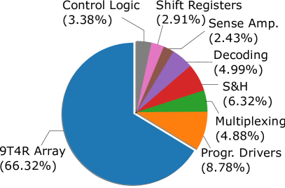
The physical layout for the proposed 9T4R-based ACAM IC is shown in Fig. 7(a), alongside some notation to provide more information on the sub-systems employed for the proof-of-concept design and showcase the approximate floorplan of the design. The physical layout of the proposed ACAM array was designed using a commercially available 180nm technology for CMOS and our in-house RRAM technology based on Pt///Pt metal oxide bi-layer metal-insulator-metal (MIM) RRAM technology. The RRAM technology employed has been shown to exhibit strong multi-bit memory operation [22]. We are replacing some rows of the RRAM-based ACAM array with rows that include conventional polysilicon-based resistor devices (based on components from the same 180nm technology). This array configuration is implemented alongside the RRAM-CMOS array for calibration purposes and readout assist purposes. Thus, the emulator array can be used asreference point when reading a standalone RRAM device for characterisation purposes after the BEOL integration. Additionally, it is used as a testing array towards helping with characterising the TXL-ACAM behaviour when different RRAM technologies are integrated and tested. Thus, the total ACAM array of this prototype IC has RRAM-based rows and polysilicon-based rows (the two sub-arrays are unified into a single array as shown in Fig. 7(a)). As shown in Fig. 8, the area utilisation of the main array covers the majority of the total IC area (approximately 66.3% of the total area). From the implemented peripherals, the programming drivers and the S&H channels are two of the largest block of the prototype IC with area usage of approximately 8.8% and 6.3%.
At the top part of the IC, the input capture peripherals (part of the analogue front-end) are included. A decoder provides phase control for the sampling operation of the parallel S&H circuit array. Based on the one-hot encoding generated by the digital control circuitry, the piecewise sampling of the analogue input is possible. Each sample is stored in one capacitor device (mimcap device). Transmission gates (TGs) are used to control the sampling of the S&H circuits. The TGs are appropriately sized (W/L = for both pMOS and nMOS devices of the TG) to enabled the fast charging of the hold capacitor to appropriate levels of charge. When all different samples of the analogue signal have been acquired, then a parallel analogue buffing supports the transmission of the analogue vector into the array (for the pattern matching operation). For the case of the programming operation of the array, the input signal is set to logic high (for =3V). The output of the array (when in normal pattern matching operation mode) is captured by a sense amplifier array. Each sense amplifier is designed as a dynamic latch comparator type of circuit effectively comparing the matchline voltage to a specific predetermined biasing voltage. Each sense amplifier outputs the results of this comparison. All sense amplifier outputs are connected in parallel to a serialiser circuit (effectively a Parallel Input Serial Output Shift Register). Thus, when the pattern recognition phase is completed, all the outputs of the sense amplifier array are loaded into the serialiser and then a bit-stream is sent through a single output pin by shifting the contents of the serialiser to this output pin.
In the characterisation mode (also referred to as programming mode), the TXL cell “disconnects” the RRAM devices from the rest of the cell and each RRAM device can be uniquely addressed through the use of accompanying “programming” nMOS devices. Effectively, during the programming/characterisation mode, the array becomes a 1T1R type of crossbar array, thus every TXL (9T4R cell) circuit becomes 2 1T1R cells. The access (for programming purposes) to each RRAM device is controlled by a 64-bit decoder which is physically placed at the bottom of the TXL array and not showcased as part of the normal programming circuitry (physically placed at the left of the TXL array). The programming logic used to generate the appropriate programming control signals and thus control the programming drivers and program/read multiplexing are implemented using (mostly) minimum size high threshold 5V MOSFET components (thus, W/L=). Buffers are necessary to increase the driving strength between the minimum sized logic and the driver circuits, to effectively control the programming MOSFET connections to TE and BE (with regards to the RRAM devices under test). The size of the programming drivers depends on the 9T4R array size (and the resistive load that is expected to be encountered in the programming paths, especially for the ones at the opposite end of the array compared to where the programming circuits exist). The estimated size is W/L= for pMOS and W/L= for nMOS devices that comprise the programming drivers.
For design validation, we performed post-layout simulation on this proof-of-concept IC after extracting the resistive and capacitive parasitics of the physical layout. Since the RRAM model used to perform pre-layout simulations is not yet adapted for parasitics extraction, for the purpose of validating the main functionality of the design post-layout, we are replacing the RRAM components with polysilicon-based resistors in a similar manner with the polysilicon-based part of the initial IC which is used for calibration and RRAM read reference. Although this is not enabling us to include the full intrinsic characteristics of the RRAM devices into our design, we are using this method to provide a baseline system analysis to prove the functionality of our array design alongside the implemented peripheral and how they are affected by resistive and capacitive parasitics. An example operation of the analogue pattern matching operation is shown in Fig. 7(b). More specifically, a part of the matchline readout vector alongside the sense amplifier classification and the array and sense amplifier control sequence is showcased. In this example operation, we are showcasing the main control signals required to read the TXL-ACAM array. The control the equalisation-evaluation cycle of the sense amplifier, with equalisation setting up the sense amp into a low power unstable state and the evaluation enabling the sense amp to settle quickly depending on the voltage threshold and the matchline charge. The is the global array enable signal that dictates the reading phase of the ACAM array during the pattern recognition phase. When the query is supplied to the array, enables the charging of the matchline for each cell that has an input that falls between the match window, as determined by the RRAM values, by controlling the pMOS as shown in Fig. 2(d). The is a global matchline control signal that dictates the reset of the matchlines by discharging them through a specific rate, which is determined by a leakage resistor implemented per matchline. The output response of the TXL-ACAM array is shown in Fig. 7(b). The matchline outputs (for this example the subset of is shown) illustrate the charging-discharging cycle of the pattern search operation. The sense amplifier output (for this example the subset of is shown) showcase the output of the dynamic latch-based circuit which effectively performs a comparison between the charging level of each matchline during the specific time when the sense amplifier evaluation starts against a provided threshold voltage which is depicted alongside the traces. For the case of our example operation, we are setting . For our design, the level indicate a pattern hit while a =5V level indicates a pattern miss. It is worth mentioning that for the specific part of the simulations showed, the same input query is used for multiple equalise-evaluate cycles of the sense amplifier. Thus, the matching line is showing only since both the equalisation the evaluations are setting it to .
V Conclusions & Discussion
In this work, we propose a RRAM-based TXL-ACAM cell design for analogue template matching at the edge. This design is using a 9T4R cell configuration to enable energy efficient ACAM applications. The cell was designed and tested using a commercially available 180nm CMOS technology and a RRAM model adapted on the physical characteristics of our in-house RRAM technology [34]. The proposed 9T4R ACAM cell design improves the tuneability of the matching windows in comparison to the state-of-the-art by using one hybrid RRAM-CMOS inverter per threshold. Also, it enables the easy accessing of each standalone RRAM device for electroforming and programming operations through the additional nMOS access devices. Finally, enables the configurable contribution of the cell to the charging matchline through the additional enable pMOS device at the comparator part of the cell. Although this results in a relatively large ACAM cell, it enables energy efficient operation due to its CMOS-oriented design of the RRAM-CMOS inverters that are used to map the matching window per cell. This results in an ACAM design that is a promising candidate for extreme edge computing.
Furthermore, a prototype IC design aimed at testing the novel 9T4R pixel cell in an ACAM macro implementation, co-designed with custom peripherals necessary for performing analogue template matching and RRAM device programming, is designed and tested in simulation using a commercial 180nm technology. The IC was designed using 5V MOSFET components from the 180nm library and was fully custom-made following the analogue design flow in Cadence Virtuoso environment. The IC was tested with RC parasitic extracted components through post-layout simulations towards further validating the proper circuit behaviour of each IC block and estimating the performance of the TXL-ACAM.
The findings in this work illustrate that the proposed 9T4R-based TXL-ACAM could be considered a promising candidate for integration into near-sensor systems for analogue template matching at the edge due to its energy efficiency and enhanced tuneability capabilities. Such solutions could greatly benefit bio-signal processing either near-sensor or in-sensor using energy efficient memory-centric accelerators and template matching engines. The design and implementation of the showcased prototype IC using high threshold 5V components enables the easy integration of different RRAM devices. Additionally, further design effort to minimise and optimise the peripherals will achieve a more compact prototype IC design. Although currently the full 5V design was selected as a versatile and extra safe method for integration with a multitude of RRAM devices, the transfer to 1.8V components will also be beneficial for power and area. Furthermore, transferring the design to a smaller MOSFET technology node, such as 90nm or 65nm, will further help with power and area. Thus, further exploration of RRAM device technologies, in the form of different device’s stack configurations, and its integration with CMOS will drive the miniaturisation of the current prototype IC. Finally, further investigation of how to integrate TXL-ACAM with additional components to test its architectural scalability for real-world applications will be an important for better assessing the competitiveness of the design. The test of scaled-up TXL-ACAM systems with real benchmarking, such as MNIST and CIFAR10, could provide an early estimation on the expected performance of the proposed design.
References
- [1] S. Hamdioui, M. Taouil, H. A. Du Nguyen, A. Haron, L. Xie, and K. Bertels, “Memristor: The enabler of computation-in-memory architecture for big-data,” 2015 International Conference on Memristive Systems, MEMRISYS 2015, pp. 9–11, 2016.
- [2] M. Wilkes, “The memory wall and the CMOS end-point,” ACM SIGARCH Computer Architecture News, pp. 1994–1996, 1995. [Online]. Available: http://dl.acm.org/citation.cfm?id=218865
- [3] S. A. McKee, “Reflections on the Memory Wall,” Proceedings of the 1st Conference on Computing Frontiers, pp. 162–167, 2004. [Online]. Available: http://doi.acm.org/10.1145/977091.977115
- [4] M. A. Zidan, J. P. Strachan, and W. D. Lu, “The future of electronics based on memristive systems,” Nature Electronics, vol. 1, no. 1, pp. 22–29, 2018. [Online]. Available: http://www.nature.com/articles/s41928-017-0006-8
- [5] L. Wang, S. Thiemjarus, B. Lo, and G. Z. Yang, “Toward A mixed-signal reconfigurable ASIC for real-time activity recognition,” Proc. 5th Int. Workshop on Wearable and Implantable Body Sensor Networks, BSN2008, in conjunction with the 5th Int. Summer School and Symp. on Medical Devices and Biosensors, ISSS-MDBS 2008, pp. 227–230, 2008.
- [6] M. Eggimann, A. Rahimi, and L. Benini, “A 5 w Standard Cell Memory-Based Configurable Hyperdimensional Computing Accelerator for Always-on Smart Sensing,” IEEE Transactions on Circuits and Systems I: Regular Papers, vol. 68, no. 10, pp. 4116–4128, 2021.
- [7] A. Menon, D. Sun, M. Aristio, H. Liew, K. Lee, and J. M. Rabaey, “A Highly Energy-Efficient Hyperdimensional Computing Processor for Wearable Multi-Modal Classification,” BioCAS 2021 - IEEE Biomedical Circuits and Systems Conference, Proceedings, 2021.
- [8] A. B. Rapeaux and T. G. Constandinou, “Implantable brain machine interfaces: first-in-human studies, technology challenges and trends,” Current Opinion in Biotechnology, vol. 72, pp. 102–111, 2021, tissue, Cell and Pathway Engineering. [Online]. Available: https://www.sciencedirect.com/science/article/pii/S095816692100183X
- [9] E. Donati and G. Valle, “Neuromorphic hardware for somatosensory neuroprostheses,” Nat Commun, vol. 15, 2024. [Online]. Available: https://www.nature.com/articles/s41467-024-44723-3
- [10] K. Ni, X. Yin, A. F. Laguna, S. Joshi, S. Dünkel, M. Trentzsch, J. Müeller, S. Beyer, M. Niemier, X. S. Hu, and S. Datta, “Ferroelectric ternary content-addressable memory for one-shot learning,” Nature Electronics, vol. 2, no. 11, pp. 521–529, 2019.
- [11] Y. Alkabani, M. Miscuglio, V. J. Sorger, and T. El-ghazawi, “OE-CAM : A Hybrid Opto-Electronic Content Addressable Memory,” arXiv:1912.02220 [physics.app-ph], vol. xx, no. xx, pp. 1–14, 2019.
- [12] K. Eshraghian, K. R. Cho, O. Kavehei, S. K. Kang, D. Abbott, and S. M. S. Kang, “Memristor MOS content addressable memory (MCAM): Hybrid architecture for future high performance search engines,” IEEE Transactions on Very Large Scale Integration (VLSI) Systems, vol. 19, no. 8, pp. 1407–1417, 2011.
- [13] X. Yin, C. Li, Q. Huang, L. Zhang, M. Niemier, X. S. Hu, C. Zhuo, and K. Ni, “FeCAM: A Universal Compact Digital and Analog Content Addressable Memory Using Ferroelectric,” IEEE Transactions on Electron Devices, vol. 67, no. 7, pp. 2785–2792, 2020.
- [14] C. E. Graves, C. Li, X. Sheng, D. Miller, J. Ignowski, L. Kiyama, and J. P. Strachan, “In-Memory Computing with Memristor Content Addressable Memories for Pattern Matching,” Advanced Materials, vol. 32, no. 37, 2020.
- [15] C. E. Graves, C. Li, X. Sheng, W. Ma, S. R. Chalamalasetti, D. Miller, J. S. Ignowski, B. Buchanan, L. Zheng, S. T. Lam, X. Li, L. Kiyama, M. Foltin, M. P. Hardy, and J. P. Strachan, “Memristor TCAMs Accelerate Regular Expression Matching for Network Intrusion Detection,” IEEE Transactions on Nanotechnology, vol. 18, pp. 963–970, 2019.
- [16] G. Yang and F. Ding, “Associative memory optimized method on deep neural networks for image classification,” Information Sciences, vol. 533, no. 4192029, pp. 108–119, 2020. [Online]. Available: https://doi.org/10.1016/j.ins.2020.05.038
- [17] G. Tanaka, R. Nakane, T. Takeuchi, T. Yamane, D. Nakano, Y. Katayama, and A. Hirose, “Spatially Arranged Sparse Recurrent Neural Networks for Energy Efficient Associative Memory,” IEEE Transactions on Neural Networks and Learning Systems, vol. 31, no. 1, pp. 24–38, 2020.
- [18] L. Chua, “If it’s pinched it’s a memristor,” Semiconductor Science and Technology, vol. 29, no. 10, pp. 1–42, 2014.
- [19] D. Ielmini and H.-S. P. Wong, “In-memory computing with resistive switching devices,” Nature Electronics, vol. 1, no. 6, pp. 333–343, 2018. [Online]. Available: http://www.nature.com/articles/s41928-018-0092-2
- [20] A. Sebastian, M. Le Gallo, G. W. Burr, S. Kim, M. Brightsky, and E. Eleftheriou, “Tutorial: Brain-inspired computing using phase-change memory devices,” Journal of Applied Physics, vol. 124, no. 11, 2018.
- [21] A. Sebastian, M. Le Gallo, R. Khaddam-aljameh, E. Eleftheriou, M. L. Gallo, R. Khaddam-aljameh, and E. Eleftheriou, “Memory devices and applications for in-memory computing,” Nature Nanotechnology, vol. 15, no. 7, pp. 529–544, 2020. [Online]. Available: http://dx.doi.org/10.1038/s41565-020-0655-z
- [22] S. Stathopoulos, A. Khiat, M. Trapatseli, S. Cortese, A. A. Serb, I. Valov, and T. Prodromakis, “Multibit memory operation of metal-oxide Bi-layer memristors,” arXiv:1704.03313 [cond-mat.mes-hall], vol. 7, no. 1, 2017.
- [23] H. Zhang, D. Zhu, W. Kang, Y. Zhang, and W. Zhao, “Stochastic Computing Implemented by Skyrmionic Logic Devices,” Physical Review Applied, vol. 13, no. 5, p. 054049, may 2020. [Online]. Available: https://journals.aps.org/prapplied/abstract/10.1103/PhysRevApplied.13.054049
- [24] C. E. Graves, W. Ma, X. Sheng, L. Zheng, S.-t. Lam, X. Li, R. Chalamalasetti, L. Kiyama, J. P. Strachan, and M. P. Hardy, “Regular Expression Matching with Memristor TCAMs for Network Security,” in Nanoscale Architectures (NANOARCH), 2018 IEEE/ACM International Symposium on, 2018.
- [25] A. Serb, A. Khiat, and T. Prodromakis, “Seamlessly Fused Digital-Analogue Reconfigurable Computing using Memristors,” Nature Communications, vol. 9, no. 2170, pp. 16–18, 2018. [Online]. Available: https://eprints.soton.ac.uk/421791/
- [26] T. Kohonen, Associative Memory, Content Addressing, and Associative Recall. Berlin, Heidelberg: Springer Berlin Heidelberg, 1980, pp. 1–37. [Online]. Available: https://doi.org/10.1007/978-3-642-96552-4_1
- [27] G. Pedretti, C. E. Graves, S. Serebryakov, R. Mao, X. Sheng, M. Foltin, C. Li, and J. P. Strachan, “Tree-based machine learning performed in-memory with memristive analog CAM,” Nature Communications, vol. 12, no. 5806, 2021.
- [28] G. Pedretti, C. E. Graves, T. Van Vaerenbergh, S. Serebryakov, M. Foltin, X. Sheng, R. Mao, C. Li, and J. P. Strachan, “Differentiable Content Addressable Memory with Memristors,” Advanced Electronic Materials, vol. 8-8, no. 2101198, 2022.
- [29] A. Ahmed, K. Park, and S. Baeg, “Resource-Efficient SRAM-Based Ternary Content Addressable Memory,” IEEE Transactions on Very Large Scale Integration (VLSI) Systems, vol. 25, no. 4, pp. 1583–1587, 2017.
- [30] P. Junsangsri, J. Han, and F. Lombardi, “Design and Comparative Evaluation of a PCM-Based CAM (Content Addressable Memory) Cell,” IEEE Transactions on Nanotechnology, vol. 16, no. 2, pp. 359–363, 2017.
- [31] C. Li, C. E. Graves, X. Sheng, D. Miller, M. Foltin, G. Pedretti, and J. P. Strachan, “Analog content-addressable memories with memristors,” Nature Communications, vol. 11, no. 1638, 2020.
- [32] S. Agwa, G. Papandroulidakis, and T. Prodromakis, “A 1T1R+2T Analog Content-Addressable Memory Pixel for Online Template Matching,” 2023 IEEE International Symposium on Circuits and Systems (ISCAS), 2023.
- [33] G. Rovere, S. Fateh, and L. Benini, “A 2.1 W event-driven wake-up circuit based on a level-crossing ADC for pattern recognition in healthcare,” 2017 IEEE Biomedical Circuits and Systems Conference, BioCAS 2017 - Proceedings, vol. 2018-Janua, pp. 1–4, 2018.
- [34] I. Messaris, A. Serb, and T. Prodromakis, “A Compact Verilog-A Memristor Switching Model,” arXiv:1703.01167, 2017. [Online]. Available: https://arxiv.org/ftp/arxiv/papers/1703/1703.01167.pdf
![[Uncaptioned image]](/html/2410.03414/assets/Figures/Figures_Short_Bio/GeorgiosPapandroulidakis.jpg) |
Georgios Papandroulidakis is a Research Associate at the Centre for Electronics Frontiers (CEF), The University of Edinburgh (UK). He received his Diploma-MEng (in 2015) and MSc (in 2017) degrees on Electronics and Computer Engineering from Democritus University of Thrace, Greece, with his diploma and MSc thesis involving the design and simulation of memristor-based circuits and systems. He completed his PhD on reconfigurable RRAM-based circuit, systems and computer architectures in 2021 (University of Southampton, UK) working on hybrid RRAM-CMOS Threshold Logic Gates -based circuit and fast prototyping of hardware test setups for on-wafer measurements. He joined the CEF group as a Research Associate in 2021 working on areas of emerging electronics and their applications such as RRAM-based Circuit and Systems, In-Memory Computing, Approximate Computing, In-Sensor and Near-Sensor Pattern Classification, and Memory-Centric Hardware Accelerator Architecture Design. His most recent research focus is on ACAM neuro-inspired systems comprised of hybrid RRAM-CMOS circuit for energy efficient analogue pattern matching. |
![[Uncaptioned image]](/html/2410.03414/assets/Figures/Figures_Short_Bio/ShadyAgwa.jpg) |
Shady Agwa (Member, IEEE) is a Research Fellow at the Centre for Electronics Frontiers (CEF), The University of Edinburgh (UK). He received his BSc and MSc degree from Assiut University (Egypt), both in Electrical Engineering. He got his PhD in Electronics Engineering from The American University in Cairo (Egypt) in 2018. Following his PhD, he joined the Computer Systems Laboratory at Cornell University (USA) as a Postdoctoral Associate for two years. In 2021, Shady joined the Centre for Electronics Frontiers at the University of Southampton (UK) as a Senior Research Fellow and then as a Research Fellow at the University of Edinburgh (UK). His research interests span across VLSI and Computer Architecture for AI using conventional and emerging technologies. His work focuses on ASIC-Driven AI Architectures with extensive expertise in In-Memory Computing, Stochastic Computing, Systolic Arrays, Beyond Von Neumann Architectures, Memories and Energy-Efficient Digital ASIC Design. |
![[Uncaptioned image]](/html/2410.03414/assets/x9.png) |
Ahmet Cirakoglu (Member, IEEE) is a PhD student at the Centre of Electronic Frontiers, Institute for Integrated Micro and Nano Systems, University of Edinburgh, United Kingdom. Prior to that, Ahmet was an RFIC design engineer at Phasor Solutions (now Hanwha Phasor) between 2017 and 2020. He received his M.Eng degree in Electrical and Electronic Engineering from Imperial College London in 2017 and M.Sc degree in Machine Intelligence for Nano-electronic Devices and Systems from University of Southampton in 2022. His research interests include design of radiation hardened, mixed-signal AI hardware accelerators, memory design with emerging non-volatile RRAM technology, electrical characterization and modelling or RRAM devices, in-memory computing and analogue circuit design. |
![[Uncaptioned image]](/html/2410.03414/assets/Figures/Figures_Short_Bio/ThemisProdromakis.jpg) |
Themis Prodromakis (Senior Member, IEEE) received the bachelor’s degree in electrical and electronic engineering from the University of Lincoln, U.K., the M.Sc. degree in microelectronics and telecommunications from the University of Liverpool, U.K., and the Ph.D. degree in electrical and electronic engineering from Imperial College London, U.K. He then held a Corrigan Fellowship in nanoscale technology and science with the Centre for Bio-Inspired Technology, Imperial College London, and a Lindemann Trust Visiting Fellowship with the Department of Electrical Engineering and Computer Sciences, University of California at Berkeley, USA. He was a Professor of nanotechnology at the University of Southampton, U.K. He holds the Regius Chair of Engineering at the University of Edinburgh and is Director of the Centre for Electronics Frontiers. He is currently a Royal Academy of Engineering Chair in emerging technologies and a Royal Society Industry Fellowship. His background is in electron devices and nanofabrication techniques. His current research interests include memristive technologies for advanced computing architectures and biomedical applications. He is a fellow of the Royal Society of Chemistry, the British Computer Society, the IET, and the Institute of Physics. |