CIF]University of Brasília, Institute of Physics and International Center of Physics, Brasília -, DF, Brazil Unicamp]State University of Campinas and Center for Computational Engineering and Sciences, Campinas , SP, Brazil UNIR]Physics Department, Federal University of Rondônia, , Porto Velho, Brazil
Raman Spectra and Excitonic Effects of the novel \ceTa2Ni3Te5 Monolayer
Abstract
We have investigated the Raman spectrum and excitonic effects of the novel two-dimensional \ceTa2Ni3Te5 structure. The monolayer is an indirect band gap semiconductor with an electronic band gap value of and , determined using GGA-PBE and HSE06 exchange-correlation functionals, respectively. Since this structure is energetically, dynamically, and mechanically stable, it could be synthesized as a free-standing material. We identify ten Raman and ten infrared active modes for various laser energies, including those commonly used in Raman spectroscopy experiments. It was also observed that the contribution of \ceNi atoms is minimal in most Raman vibrational modes. In contrast, most infrared vibrational modes do not involve the vibration of the \ceTa atoms. As far as the optical properties are concerned, this monolayer shows a robust linear anisotropy, an exciton binding energy of , and also presents a high reflectivity in the ultraviolet region, which is more intense for linear light polarization along the direction.
1 Introduction
Graphene’s experimental realization in the early 2000s 1, 2 marked a new frontier in solid-state physics and materials science. Graphene exhibits unique electronic and mechanical properties.3 Graphene also renewed the interest in other new 2D materials, some of which possess interesting properties 4, 5, 6, 7 and functionalities,8, 9, 10. Examples include the combination of different monolayers to form van der Waals (vdW) heterojunctions, allowing to tune a wide variety of properties 11, 12, 13. Unlike some bulk systems, the quantum confinement in those materials makes the excitonic quasi-particle effects relevant for a reliable characterization of their linear optical response,9, 14 requiring sophisticated experimental and theoretical approaches.
Recently, vdW layered materials of the \ceA2M_1,3X5 (\ceA=\ceTa,Nb; \ceM=\cePd,Ni and \ceX=\ceSe, Te) family have received attention due to exotic properties, such as the quantum spin Hall effect in the \ceTa2Pd3Te5 monolayer,15, 16 excitons in \ceTa2NiSe5,17, 18 and superconductivity in \ceNb2Pd3Te5 and doped \ceTa2Pd3Te5 structures.19 Both \ceTa2Pd3Te5 and \ceTa2Ni3Te5, which have been experimentally created in their layered bulk form,20, 21, exhibit intriguing topological properties.22, 20
Ta2Pd3Te5 and \ceTa2Ni3Te5 share the same crystal structure,23 consisting of rhombus-like \ceTa2Pd2(\ceTa2Ni2) clusters that act as building blocks within each layer. These clusters are linked into 1D chains, then loosely connected to form a 2D layer.24 Despite the structural similarities, both compounds exhibit distinct properties due to differences in the band gap of their normal states;23 \ceTa2Pd3Te5 is classified as an excitonic insulator23, 25 whereas \ceTa2Ni3Te5 is a small band gap semiconductor, with an electronic band gap of in its bulk form.20, 23
In particular, \ceTa2Ni3Te5 exhibits topological phase transitions under pressure and is also predicted to undergo a similar transition under strain 15, 26, showing potential for various practical applications. In addition, \ceTa2Ni3Te5 also presents an in-plane anisotropy, which originates from its anisotropic crystal lattice and point group symmetry;21; this leads to a dependency of its electronic, optical, and thermal properties on the crystal orientation, hence enabling its use in anisotropic photoelectric and thermoelectric devices, similar to black phosphorus. 27, 28, 21 In fact, Harrison and co-workers investigated this in-plane anisotropy through polarized Raman spectroscopy, establishing a clear correlation between the structural and optical in-plane anisotropies in exfoliated few-layer \ceTa2Ni3Te5.21
In this work, we systematically investigated the electronic, optical, excitonic, and vibrational properties of the \ceTa2Ni3Te5 monolayer, combining first-principles methods with a semi-empirical approach for computational characterization. As indicated by the phonon dispersion spectrum, the dynamical stability was used to identify the monolayer’s active Raman and IR vibrational modes. Our results reveal an anisotropic behavior consistent with the analogous bulk structure. This anisotropy extends to the optical properties, where the optical response is highly sensitive to light polarization due to quantum confinement along the perpendicular basal direction.
2 Computational details
The structural, electronic, and vibrational properties were obtained from simulations based on density functional theory (DFT) 29, 30 methods within the scope of the generalized gradient approximation (GGA)31, 32, 33, 34, 35 using the exchange-correlation (XC) functional proposed by Perdew–Burke–Ernzerhof (PBE).31, 36 Because PBE underestimates the electronic band gap,37, 38 causes self-interaction problems, and gives a poor description of weak interactions,39, 40, 41 we employed the hybrid XC functional proposed by Heyd–Scuseria–Ernzerhof (HSE06) 42, 43 to obtain a reasonable correction to the electronic band structure.
The Kohn–Sham (KS) equations were solved through the projector augmented-wave method (PAW),44, 45 using the Vienna Ab Initio Simulation Package (VASP).46, 47 For all simulations, a total energy convergence criterion of was employed for the self-consistent cycle. To obtain the equilibrium structures, we optimize the stress tensor and minimize the inter-atomic forces with a plane-wave cutoff energy of until the atomic forces on each atom were less than . We compute other properties with a lower cutoff energy of .
For the integration of the Brillouin zone (BZ), we used a k-mesh of for the electronic band structure and structural optimization calculations and a denser k-mesh for the density of states (DOS) calculations. A vacuum distance of was added along the -direction to eliminate spurious interactions with the structure’s mirror images.
We used the Quantum Espresso (QE) package 48, 49 to obtain the phonon dispersion and the phonon density of states of the \ceTa2Ni3Te5 monolayer over the entire BZ, using truncated Coulomb interactions, -imposed by the assumeisolated flag,- 50; this method is beneficial to treat two-dimensional systems by avoiding the interaction with repeated images during the phonon calculation. The QERaman code,51 interfaced with QE, was then used to determine which of the sixty vibrational modes at the high-symmetry point are Raman (R) active.
Determining the intensity of the R-active modes at several laser energy values can also be inferred, thus allowing a direct comparison with experimental data. These calculations were performed using a plane-wave energy cutoff, with a PBE exchange functional embedded in Troullier-Martins (TM) pseudo-potentials (PPs) 52, 53. A k-mesh and a small electronic temperature of were added to smoothen the numerical solutions and help reach convergence. It is important to note that the spin-orbit coupling (SOC) has been added self-consistently, only to point out the variation in the band structure. The phonon dispersion, excitonic effects, and Raman spectra were examined without including the SOC.
The maximally localized Wannier function Tight Binding (MLWF-TB) method was exploited to describe the electronic states and determine the MLWF-TB Hamiltonian using the Wannier90 code 54. The optical properties are then evaluated within the scope of the independent particle approximation (IPA) and through the solution of the Bethe-Salpeter equation (BSE) 55 using the WanTiBEXOS package.56 It should be noted that the MLWF-TB Hamiltonian was obtained at an HSE06 level, directly from VASP, with a k-mesh of considering and orbital projections for \ceTa and \ceNi, and and projections for \ceTe. The BSE was solved using the Coulomb truncated 2D potential (V2DT)57 with a k-mesh taking into account the lowest 12 conduction bands and the highest 12 valence bands; also a smearing value of was applied for the dielectric function computation.
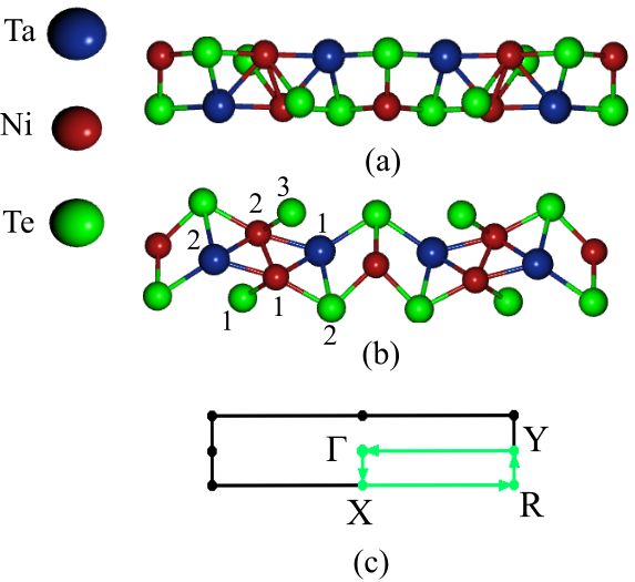
3 Geometry and Structural Properties
The top and side views of the monolayer, as well as its two-dimensional (2D) Brillouin zone (BZ), are illustrated in Fig. 1. The \ceTa2Ni3Te5 monolayer pertains to the Pm space-group with equilibrium lattice constants a= and b=, consistent with the bulk experimental data.21 The structure has two Ni-Te bond lengths, with = and =. On the other hand, =, =, = and =. The cohesive energy per atom (Ecoh/atom), resulting from the arrangements of the different atoms in the ground state of the \ceTa2Ni3Te5 monolayer, is defined via :
where Etot is the total energy of the monolayer and ETa, ETe, and ENi are the energies of isolated Ta, Te, and Ni atoms, respectively; the number ’20’ in the denominator refers to the total number of atoms in the unit cell. Our calculations predict an Ecoh/atom=, which, in principle, means that the structure is energetically favorable.
4 Mechanical Properties
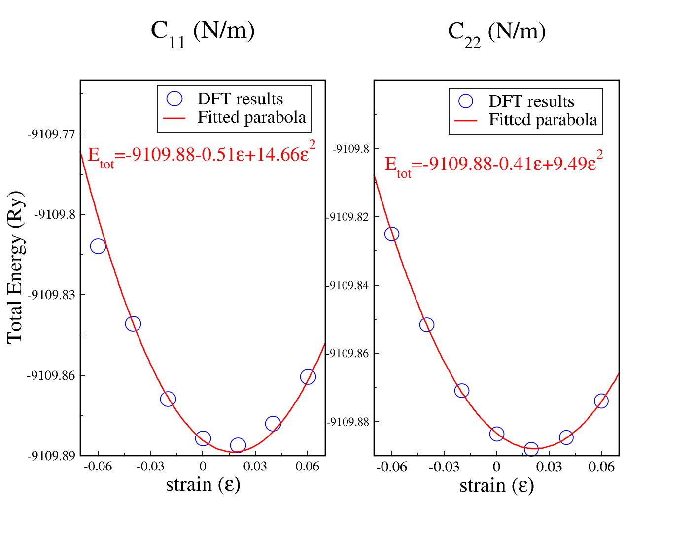
Studying the structure’s response to different strain types lets us obtain the mechanical properties of the \ceTa2Ni3Te5 monolayer. Since the unit cell is rectangular, a strain along the and directions will cause a change in the lattice parameters along these directions without actually varying the rectangular unit cell. As a consequence, the C11 and C22 elastic constants can be determined. A third elastic constant, C12, results from a biaxial strain within the plane that also preserves the rectangular unit cell.
Fig. 2 exhibits the variation of the total energy (Etot) under compressive and tensile strain () values, ranging from -6 to 6 and applied along the and directions. The DFT values are fitted to second-degree polynomials in , from which C11 and C22 were determined as , being the thickness of the \ceTa2Ni3Te5 monolayer. In this way, C11 and C22 will be vacuum-independent and in units of N/m.
From our calculations C11=, C22=, and C12=. Furthermore, the Poisson ratios = C12/ C11 and = C12/ C22 are 0.22 and 0.34, respectively. These values are vacuum-independent, exhibiting an anisotropy along the and directions. They also illustrate the mechanical stability of the structure with C 0, C 0 and and 0.5. A positive Poisson’s ratio confirms that the material is non-auxetic, contracting along the transverse direction when subjected to tensile forces.
5 Electronic Band structure and Density of States (DOS)
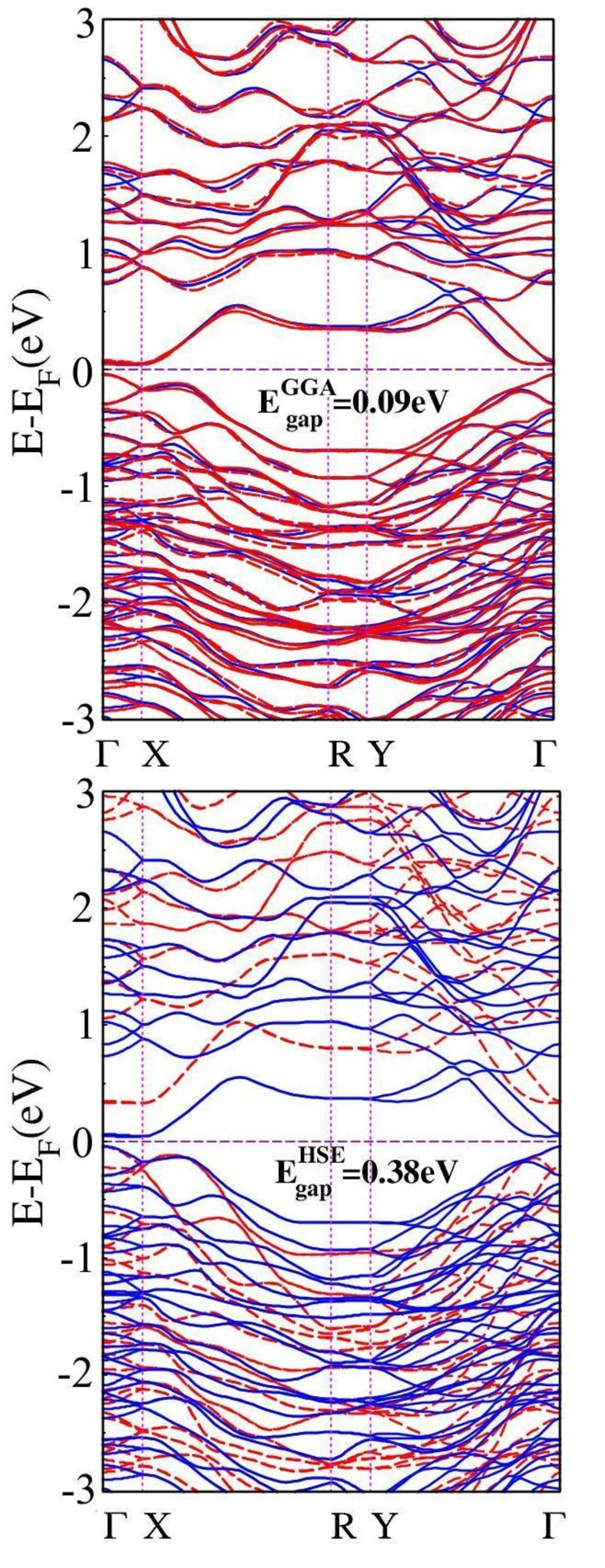

Our calculations show that the top of the valence band (VBM) occurs at the point, while the bottom of the conduction band (CBM) is at a point along the -X path. Fig. 3 demonstrates that the \ceTa2Ni3Te5 monolayer is a semiconductor with an indirect small electronic band gap of . This result is consistent with Ref. 22 (). The density of states (DOS) presented in Fig. 4 shows that within the considered energy range, both the valence and the conduction bands are mainly contributed by the orbitals of \ceNi and \ceTa, and the orbitals of \ceTe. More specifically, the most prominent DOS of the valence bands comes from the orbitals of \ceNi; in contrast, the corresponding DOS of the conduction bands is primarily influenced by the orbitals of the \ceTa atoms.
It is essential to mention that the bulk \ceTa2Ni3Te5 investigated in Jiang’s work,23 confirms the semiconducting nature of this material with a small band gap of using the Projector Augmented Wave (PAW) method 44 with a modified Becke-Johnson functional 58, 59 to describe the exchange potential. On the other hand, the 2D analog has a band gap three (twelve) times larger on a PBE (HSE06) level.
6 Phonon dispersion and Raman and IR Active Modes
Phonon calculations were carried out at the high-symmetry point to obtain the modes of vibration of the monolayer. Since the unit cell contains 20 atoms, we expect 60 vibrational modes, the first three of which are acoustic (A) modes and the remaining 57 are optical (O) ones. At the point, the modes decompose into:
The three acoustic modes belong to the B1, B2, and A1 symmetries, and 10 out of the 20 A1 modes are Raman (R) active.
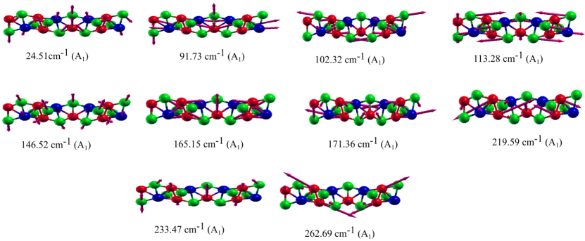
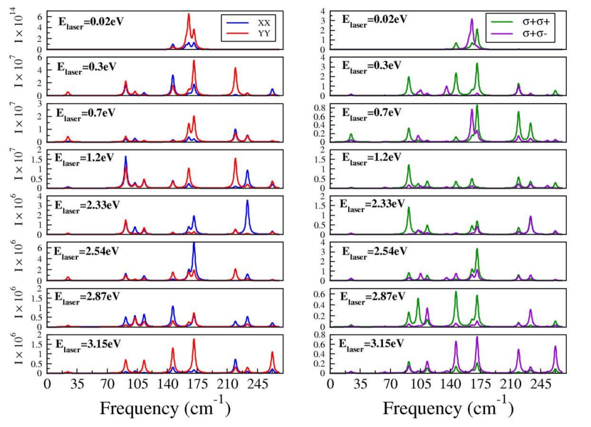
We have estimated the Raman spectra for linearly and circularly polarized light to determine these modes using several laser energy values ranging from the infrared to the ultraviolet regimes. The results are presented in Fig. 5. Our results are based on the assumption that the incident and scattered polarization vectors are parallel and that linearly polarized light propagates in a direction perpendicular to the plane of the \ceTa2Ni3Te5 monolayer. Only three peaks can be detected for laser energies (Elaser) as low as . As Elaser increases, other peaks emerge, varying in intensity. All in all, we can identify ten such peaks. Focusing on Elaser=, the peaks appear at , , , , , , , , , and .
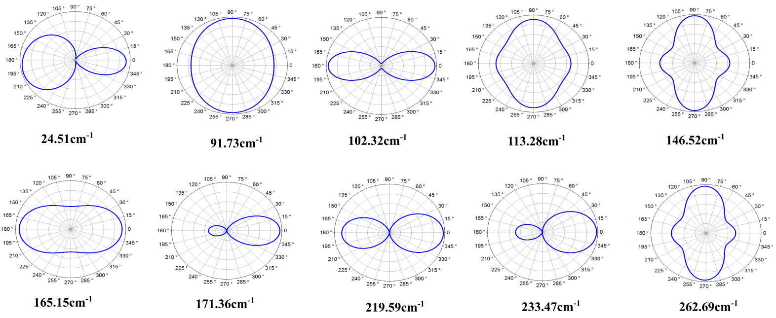
The Raman active modes are presented in Fig. 6. We note that most of the vibrational modes do not exhibit the displacement of the \ceNi atoms. On the other hand, mode 5 is mainly contributed by the vibration of the \ceTe atoms. Fig. 7 shows the Raman intensity for circularly polarized light for the ten Raman active modes. The intensity of mode 3 reaches its maximum for polarization angles = or , that is, along the x-directions. Modes 6, 7, 8, and 9 only present maxima at = . In contrast, the intensity maxima of modes 2, 4, 5, and 10 occur when and =, that is, along the y directions, with mode 2 being quasi-isotropic. Mode 1 is an entirely distinct case where the maximum does not occur at , but rather at =.
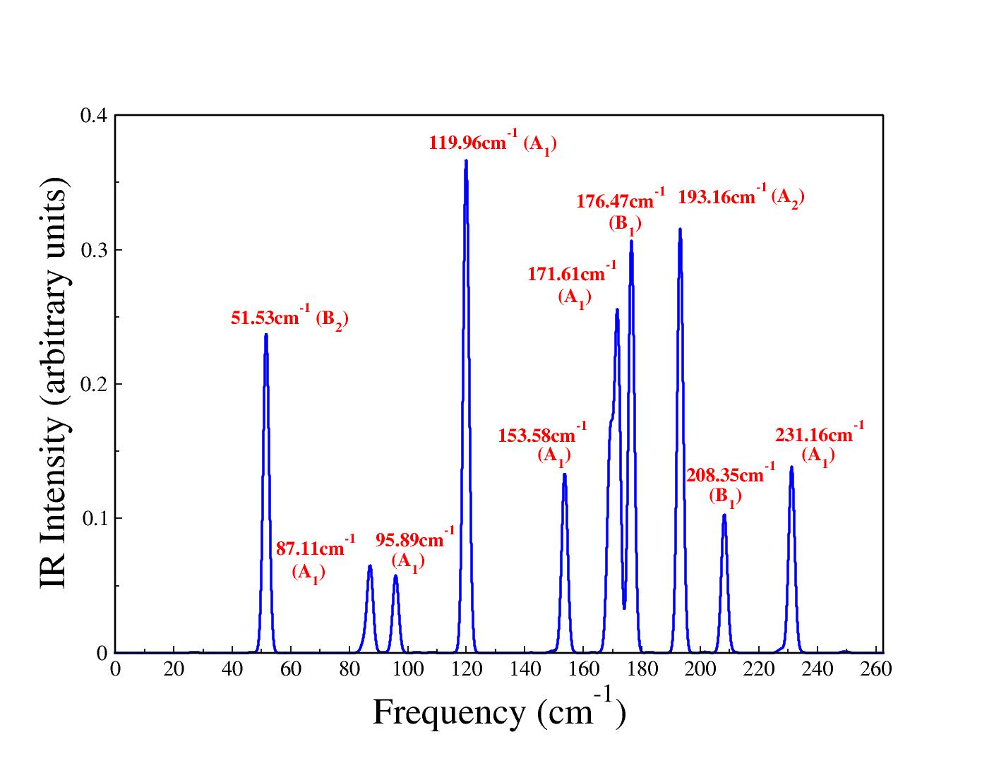
We have further calculated the IR intensities presented in Fig. 8. The results indicate that ten of the remaining modes are IR-active. More specifically, peaks of distinct intensities occur at , , , , , , , , , and . Due to the closeness of the and IR frequencies to those of the Raman active ones ( and ), we speculate that these modes can be both IR+R active.
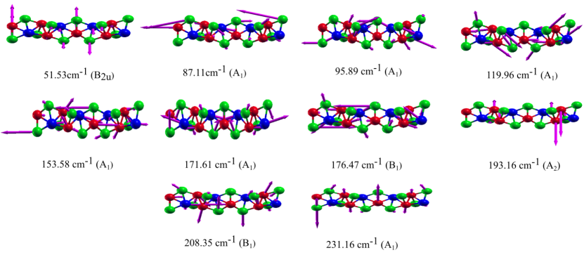
The atomic vibrations of the active modes in IR, shown in Fig. 9, belong to the symmetries A1, B1, and B2u. Modes 1 and 8 almost vibrate along the direction and are composed mainly of the vibrations of the Te and Ni atoms. The vibration of the Ta atoms is virtually absent in all IR modes.
Ref. 21 investigated the Raman active modes of few-layer (FL) \ceTa2Ni3Te5 flakes, which were composed of two monolayers. To our knowledge, no work has yet discussed the monolayered structure. In total, fifteen modes have been experimentally observed for the FL \ceTa2Ni3Te5 system emerging at , , , , , , , , , , , , , , and . Some of these modes disappeared in the Raman spectrum of the monolayer, such as the , , , and while others appeared such as the .
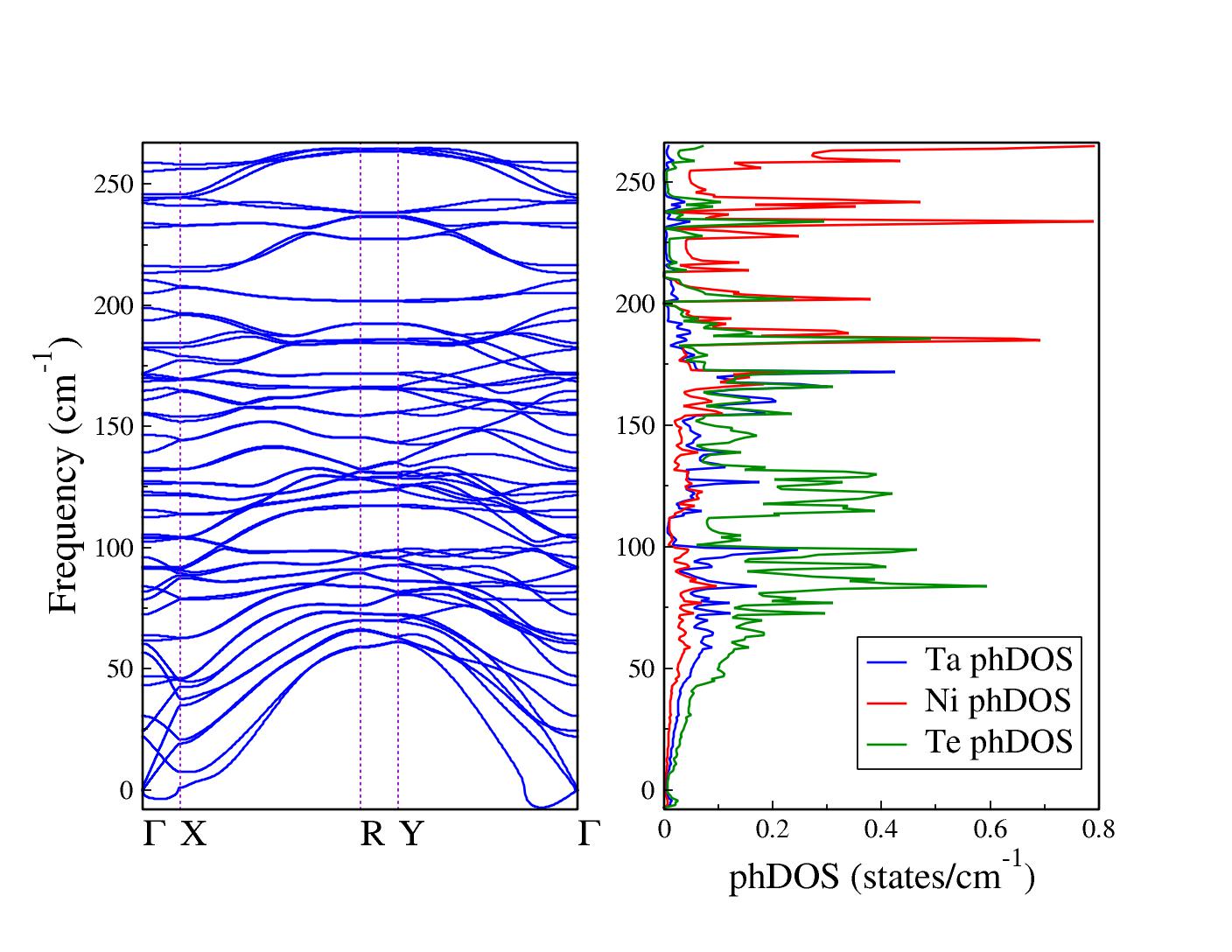
To determine the overall contributions of the \ceTa, \ceNi, and \ceTe atoms, the phonon density of states (phDOS) is plotted for the different phonon mode regimes, as demonstrated in Fig. 10. The phononic band structure, also displayed in Fig. 10, shows some slight negative frequencies in the flexural mode, not exceeding , near the point along the Y- path. More minor negative frequencies, not ultrapassing , extend along the -X path. These frequencies do not indicate a dynamical instability of the monolayer but instead represent numerical inaccuracies due to the diagonalization of the dynamical matrix. The phDOS exhibits the dominant contribution of the \ceTe atoms up to . For modes of higher frequencies, it is evident that the \ceNi atoms contribute the most.
7 Excitonic and Optical Properties
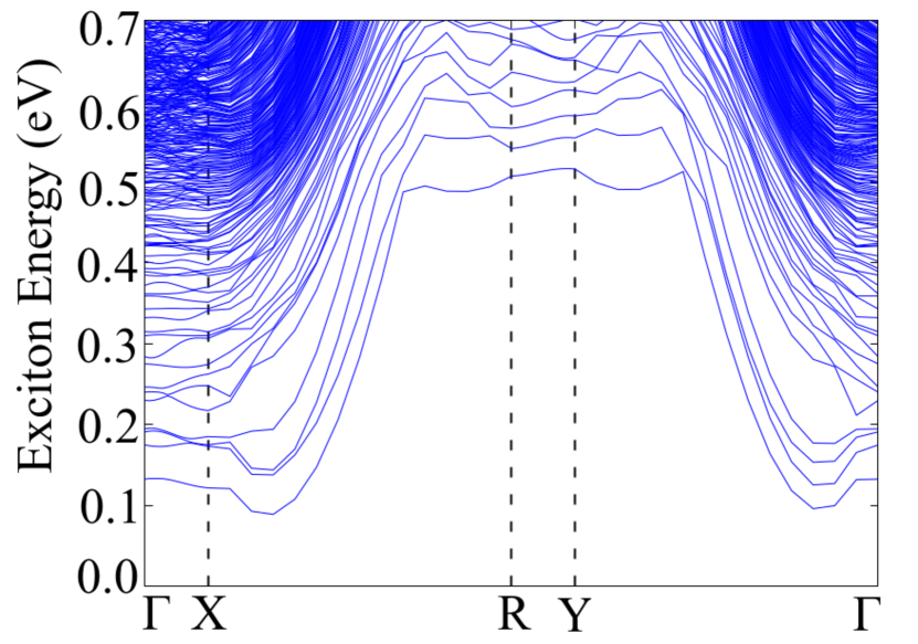
From the excitonic band structure, shown in Fig. 11, we can observe that the exciton ground state is indirect, with an exciton momentum between the and high symmetry points and an exciton binding energy of which lies in the expected range for 2D materials.9 The direct exciton ground state, located at , has a gap and corresponds to the optical band gap. The presence of an indirect exciton ground state suggests the possibility of phonon-assisted optical transitions with excitation energies lower than the optical band gap; in fact, the difference between the exciton ground state and optical band gap is very small, which makes it difficult to identify both peaks in the optical spectrum.
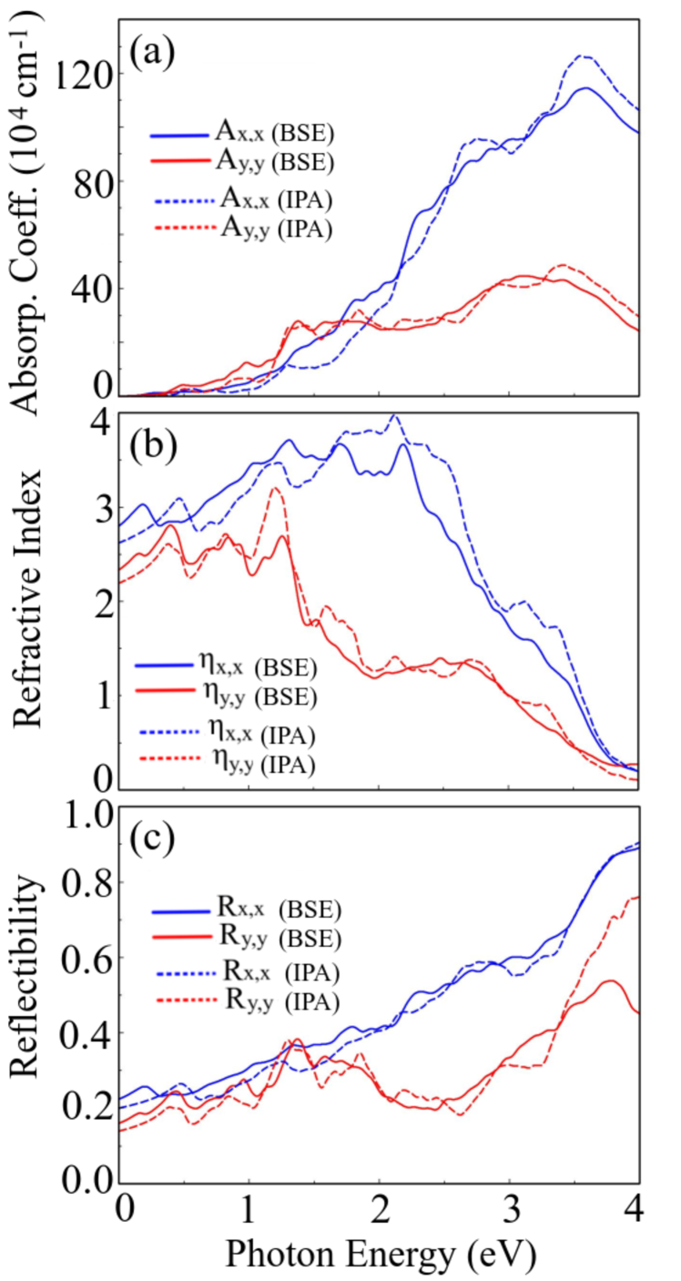
The linear optical response of the \ceTa2Ni3Te5 monolayer is shown in Fig. 12, with (BSE - solid curves) and without (IPA - dashed curves) excitonic effects for linearly polarized light along the (blue curves) and directions (red curves). From the absorption spectrum, shown in Fig. 12(a), we can observe that for lower optical excitations in the infrared and at the beginning of the visible spectrum (around ), the optical response is very similar, independent of the light polarization. Conversely, we can see that, for higher excitations, the system absorbs with a higher intensity for the polarization case, showing a significant optical anisotropy in the visible and ultraviolet regions. The excitonic effects result in a slight red shift in the absorption spectrum, yet these quasi-particle effects do not considerably change the spectrum shape and intensities.
The refractive index and reflectivity are shown in Figs. 12 (b) and (c), respectively. The refractive index is higher for polarization along the direction. It registers the highest value in the visible region, decreasing as the photon energy moves to the ultraviolet region. Although the excitonic effects are evident, the changes are inconsiderable. Regarding the reflectivity, the opposite happens, as this factor is enhanced as the photon excitation energy increases. For photon energies higher than , the optical anisotropy becomes more evident, showing a quasi-total reflectivity for photons closer to the ultra-violet region for light polarized along the direction. For a polarization along the direction and at BSE (IPA) level, the reflectivity at is . The comparison between BSE and IPA optical responses is vital as the excitonic effects are susceptible to the substrate where the monolayer could be placed. The higher the dielectric constant of the substrate is, the lower the excitonic effects 9.
Besides, we have observed an interesting behavior when photon energy increases and is in the ultraviolet (UV) region; the absorption and refractive index tend to decrease while reflectivity increases, indicating that the material minimally absorbs ultraviolet radiation and has a high potential for reflection. This comportment is particularly relevant for materials used to fabricate ultraviolet-blocking devices.
8 Conclusions
The Raman spectra, the excitonic effect, and the dynamical and mechanical stabilities of the novel \ceTa2Ni3Te5 monolayer have been investigated. The monolayer is an indirect small band gap semiconductor of () band gap value within the PBE (HSE06) approximation. It exhibits anisotropic properties, registering different mechanical responses to strain when applied along the and directions. It is also dynamically stable, except for minor negative frequencies near the point in the corresponding phonon dispersion spectrum, primarily due to numerical inaccuracies in the dynamical matrix diagonalization process. Its phonon DoS illustrates the dominant contributions of the Te and Ni atoms to the vibrational modes of the monolayer.
The Raman spectrum exhibits an increase in the number of peaks upon increasing the laser energy values. We have identified ten peaks corresponding to this monolayer’s ten Raman active modes for a typical laser energy of . We have further determined ten infrared modes characterized by the predominant vibrations of the \ceTe and \ceNi atoms.
The excitonic band structure for this monolayer possesses a binding energy within the expected range for 2D materials and an indirect exciton ground state, which is a signature of the possibility of the occurrence of phonon-assisted optical transitions with excitation energies smaller than the optical bandgap. Additionally, the system is highly anisotropic, causing an optical response dependent on the incident light polarization. Moreover, the system shows a higher reflectivity for light polarized along the direction in the visible and ultraviolet regions, making the \ceTa2Ni3Te5 monolayer appropriate as a polarizing filter.
The authors are grateful for the computational resources provided by Centro Nacional de Processamento de Alto Desempenho in São Paulo-CENAPAD-SP (proj 897, 909 and 950) and the Lobo Carneiro HPC (NACAD) at the Federal University of Rio de Janeiro (UFRJ) (proj 133 and 135). A.C.D. also thanks the financial support from National Council for Scientific and Technological Development (CNPq, grant number and ), Federal District Research Support Foundation (FAPDF, grants number and ) and PDPG-FAPDF-CAPES Centro-Oeste (grant ). RMT and DSG acknowledge support from CNPq and the Center for Computational Engineering and Sciences at Unicamp, FAPESP/CEPID Grant (). Elie A. Moujaes would like to thank the financial support of the Brazilian National Council for Scientific and Technological Development CNPq, grant number .
References
- Novoselov et al. 2004 Novoselov, K. S.; Geim, A. K.; Morozov, S. V.; Jiang, D.; Zhang, Y.; Dubonos, S. V.; Grigorieva, I. V.; Firsov, A. A. Electric Field Effect in Atomically Thin Carbon Films. Science 2004, 306, 666–669, DOI: 10.1126/science.1102896
- Geim and Novoselov 2007 Geim, A. K.; Novoselov, K. S. The rise of graphene. Nature Materials 2007, 6, 183–191, DOI: 10.1038/nmat1849
- Wang et al. 2012 Wang, Q. H.; Kalantar-Zadeh, K.; Kis, A.; Coleman, J. N.; Strano, M. S. Electronics and optoelectronics of two-dimensional transition metal dichalcogenides. Nature Nanotechnology 2012, 7, 699–712, DOI: 10.1038/nnano.2012.193
- Correa et al. 2020 Correa, J. H.; Dias, A. C.; Villegas-Lelovsky, L.; Fu, J.; Chico, L.; Qu, F. Anisotropy of the spin-polarized edge current in monolayer transition metal dichalcogenide zigzag nanoribbons. Physical Review B 2020, 101, DOI: 10.1103/physrevb.101.195422
- Lu et al. 2022 Lu, J.; Qu, F.; Zeng, H.; Cavalheiro Dias, A.; Bradão, D. S.; Ren, J. Intrinsic Valley Splitting and Direct-to-Indirect Band Gap Transition in Monolayer HfZrSiCO2. The Journal of Physical Chemistry Letters 2022, 13, 5204–5212, DOI: 10.1021/acs.jpclett.2c01090
- Moujaes and Diery 2019 Moujaes, E. A.; Diery, W. Thermoelectric properties of 1 T monolayer pristine and Janus Pd dichalcogenides. Journal of Physics: Condensed Matter 2019, 31, 455502, DOI: 10.1088/1361-648X/ab347a
- Moujaes and Diery 2021 Moujaes, E. A.; Diery, W. Optical properties and stability of new two-dimensional allotropes of PdS2, PdSe2 and PdSSe monolayers. Physica E: Low-dimensional Systems and Nanostructures 2021, 128, 114611, DOI: 10.1016/j.physe.2020.114611
- Dias et al. 2018 Dias, A. C.; Qu, F.; Azevedo, D. L.; Fu, J. Band structure of monolayer transition-metal dichalcogenides and topological properties of their nanoribbons: Next-nearest-neighbor hopping. Physical Review B 2018, 98, DOI: 10.1103/physrevb.98.075202
- Dias et al. 2021 Dias, A. C.; Bragança, H.; de Mendonça, J. P. A.; Da Silva, J. L. F. Excitonic Effects on Two-Dimensional Transition-Metal Dichalcogenide Monolayers: Impact on Solar Cell Efficiency. ACS Applied Energy Materials 2021, 4, 3265–3278, DOI: 10.1021/acsaem.0c03039
- Dias et al. 2022 Dias, A. C.; Bragança, H.; Lima, M. P.; Da Silva, J. L. F. First-principles investigation of the role of Cr in the electronic properties of the two-dimensional \ceMo_xCr_1-xSe2 and \ceW_xCr_1-xSe2 alloys. Physical Review Materials 2022, 6, DOI: 10.1103/physrevmaterials.6.054001
- Besse et al. 2021 Besse, R.; Silveira, J. F. R. V.; Jiang, Z.; West, D.; Zhang, S.; Da Silva, J. L. F. Beyond the Anderson rule: importance of interfacial dipole and hybridization in van der Waals heterostructures. 2D Materials 2021, 8, 041002, DOI: 10.1088/2053-1583/ac1902
- Silveira et al. 2021 Silveira, J. F. R. V.; Besse, R.; Da Silva, J. L. F. Stacking Order Effects on the Electronic and Optical Properties of Graphene/Transition Metal Dichalcogenide Van der Waals Heterostructures. ACS Applied Electronic Materials 2021, 3, 1671–1680, DOI: 10.1021/acsaelm.1c00009
- Silveira et al. 2022 Silveira, J. F. R. V.; Besse, R.; Dias, A. C.; Caturello, N. A. M. S.; Da Silva, J. L. F. Tailoring Excitonic and Optoelectronic Properties of Transition Metal Dichalcogenide Bilayers. The Journal of Physical Chemistry C 2022, 126, 9173–9184, DOI: 10.1021/acs.jpcc.2c02023
- Moujaes and Dias 2023 Moujaes, E. A.; Dias, A. C. On the excitonic effects of the 1T and 1OT phases of \cePdS2, \cePdSe2, and \cePdSSe monolayers. Journal of Physics and Chemistry of Solids 2023, 182, 111573, DOI: 10.1016/j.jpcs.2023.111573
- Guo et al. 2021 Guo, Z.; Yan, D.; Sheng, H.; Nie, S.; Shi, Y.; Wang, Z. Quantum spin Hall effect in \ceTa2M3Te5 (M=Pd,Ni). Phys. Rev. B 2021, 103, 115145, DOI: 10.1103/PhysRevB.103.115145
- Wang et al. 2021 Wang, X.; Geng, D.; Yan, D.; Hu, W.; Zhang, H.; Yue, S.; Sun, Z.; Kumar, S.; Schwier, E. F.; Shimada, K.; Cheng, P.; Chen, L.; Nie, S.; Wang, Z.; Shi, Y.; Zhang, Y.-Q.; Wu, K.; Feng, B. Observation of topological edge states in the quantum spin Hall insulator \ceTa2Pd3Te5. Phys. Rev. B 2021, 104, L241408, DOI: 10.1103/PhysRevB.104.L241408
- Wakisaka et al. 2009 Wakisaka, Y.; Sudayama, T.; Takubo, K.; Mizokawa, T.; Arita, M.; Namatame, H.; Taniguchi, M.; Katayama, N.; Nohara, M.; Takagi, H. Excitonic Insulator State in \ceTa2SiNe5 Probed by Photoemission Spectroscopy. Phys. Rev. Lett. 2009, 103, 026402, DOI: 10.1103/PhysRevLett.103.026402
- Lu et al. 2017 Lu, Y. F.; Kono, H.; Larkin, T. I.; Rost, A. W.; Takayama, T.; Boris, A. V.; Keimer, B.; Takagi, H. Zero-gap semiconductor to excitonic insulator transition in \ceTa2NiSe5. Nature Communications 2017, 8, DOI: 10.1038/ncomms14408
- Higashihara et al. 2021 Higashihara, N.; Okamoto, Y.; Yoshikawa, Y.; Yamakawa, Y.; Takatsu, H.; Kageyama, H.; Takenaka, K. Superconductivity in \ceNb2Pd3Te5 and Chemically-Doped \ceTa2Pd3Te5. Journal of the Physical Society of Japan 2021, 90, 063705, DOI: 10.7566/jpsj.90.063705
- Zhang et al. 2024 Zhang, P.; Dong, Y.; Yan, D.; Jiang, B.; Yang, T.; Li, J.; Guo, Z.; Huang, Y.; Haobo; Li, Q.; Li, Y.; Kurokawa, K.; Wang, R.; Nie, Y.; Hashimoto, M.; Lu, D.; Jiao, W.-H.; Shen, J.; Qian, T.; Wang, Z.; Shi, Y.; Kondo, T. Spontaneous Gap Opening and Potential Excitonic States in an Ideal Dirac Semimetal \ceTa2Pd3Te5. Physical Review X 2024, 14, DOI: 10.1103/physrevx.14.011047
- Harrison et al. 2024 Harrison, K.; Jeff, D. A.; DeStefano, J. M.; Peek, O.; Kushima, A.; Chu, J.-H.; Gutiérrez, H. R.; Khondaker, S. I. In-Plane Anisotropy in the Layered Topological Insulator Ta2Ni3Te5 Investigated via TEM and Polarized Raman Spectroscopy. ACS Nano 2024, 18, 4811–4821, DOI: 10.1021/acsnano.3c09527
- Guo et al. 2022 Guo, Z.; Deng, J.; Xie, Y.; Wang, Z. Quadrupole topological insulators in Ta2M3Te5 (M=Ni, Pd) monolayers. npj Quantum Materials 2022, 7, DOI: 10.1038/s41535-022-00498-8
- Jiang et al. 2024 Jiang, B.; Yao, J.; Yan, D.; Guo, Z.; Qu, G.; Deng, X.; Huang, Y.; Ding, H.; Shi, Y.; Wang, Z.; Qian, T. Surface doping manipulation of the insulating ground states in Ta2Pd3Te5 and Ta2Ni3Te5. Chinese Physics B 2024, 33, 067402, DOI: 10.1088/1674-1056/ad362e
- Tan et al. 2024 Tan, H.; Zhang, Y.; Zhao, Z.; Wang, C.; Zhang, R.; Wang, S.; Ma, X.; Feng, Y.; Gu, M.; Lu, Y.; Jiang, J.; Zhang, S.; Xiang, B. Giant in-plane vibrational and transport anisotropy in van der Waals Ta2Ni3Te5. Science China Materials 2024, 67, 2201–2209, DOI: 10.1007/s40843-023-2817-x
- Yao et al. 2024 Yao, J.; Sheng, H.; Zhang, R.; Pang, R.; Zhou, J.-J.; Wu, Q.; Weng, H.; Dai, X.; Fang, Z.; Wang, Z. Excitonic Instability in Ta2Pd3Te5 Monolayer. Chinese Physics Letters 2024, DOI: 10.1088/0256-307x/41/9/097101
- Yang et al. 2023 Yang, H.; Zhou, Y.; Wang, S.; Wang, J.; Chen, X.; Zhang, L.; Xu, C.; Yang, Z. Pressure-induced nontrivial Z2 band topology and superconductivity in the transition metal chalcogenide \ceTa2Ni3Te5. Physical Review B 2023, 107, DOI: 10.1103/physrevb.107.l020503
- Fei et al. 2014 Fei, R.; Faghaninia, A.; Soklaski, R.; Yan, J.-A.; Lo, C.; Yang, L. Enhanced Thermoelectric Efficiency via Orthogonal Electrical and Thermal Conductances in Phosphorene. Nano Letters 2014, 14, 6393–6399, DOI: 10.1021/nl502865s
- Luo et al. 2015 Luo, Z.; Maassen, J.; Deng, Y.; Du, Y.; Garrelts, R. P.; Lundstrom, M. S.; Ye, P. D.; Xu, X. Anisotropic in-plane thermal conductivity observed in few-layer black phosphorus. Nature Communications 2015, 6, DOI: 10.1038/ncomms9572
- Hohenberg and Kohn 1964 Hohenberg, P.; Kohn, W. Inhomogeneous Electron Gas. Phys. Rev. 1964, 136, B864–B871, DOI: 10.1103/physrev.136.b864
- Kohn and Sham 1965 Kohn, W.; Sham, L. J. Self-Consistent Equations Including Exchange and Correlation Effects. Physical Review 1965, 140, A1133–A1138, DOI: 10.1103/physrev.140.a1133
- Perdew et al. 1996 Perdew, J. P.; Burke, K.; Ernzerhof, M. Generalized gradient approximation made simple. Physical review letters 1996, 77, 3865, DOI: 10.1103/physrevlett.77.3865
- Wu and Cohen 2006 Wu, Z.; Cohen, R. E. More accurate generalized gradient approximation for solids. Physical Review B 2006, 73, 235116, DOI: 10.1103/physrevb.73.235116
- Boese et al. 2000 Boese, A. D.; Doltsinis, N. L.; Handy, N. C.; Sprik, M. New generalized gradient approximation functionals. The Journal of Chemical Physics 2000, 112, 1670–1678, DOI: 10.1063/1.480732
- Perdew 1991 Perdew, J. P. Generalized gradient approximations for exchange and correlation: A look backward and forward. Physica B: Condensed Matter 1991, 172, 1–6, DOI: 10.1016/0921-4526(91)90409-8
- Burke et al. 1998 Burke, K.; Perdew, J. P.; Wang, Y. Derivation of a generalized gradient approximation: The PW91 density functional. In Electronic Density Functional Theory: recent progress and new directions; Springer, 1998; pp 81–111, DOI: 10.1007/978-1-4899-0316-7_7
- Perdew and Yue 1986 Perdew, J. P.; Yue, W. Accurate and simple density functional for the electronic exchange energy: Generalized gradient approximation. Physical review B 1986, 33, 8800, DOI: 10.1103/physrevb.33.8800
- Cohen et al. 2008 Cohen, A. J.; Mori-Sánchez, P.; Yang, W. Fractional charge perspective on the band gap in density-functional theory. Physical Review B 2008, 77, DOI: 10.1103/physrevb.77.115123
- Crowley et al. 2016 Crowley, J. M.; Tahir-Kheli, J.; Goddard, W. A. Resolution of the Band Gap Prediction Problem for Materials Design. The Journal of Physical Chemistry Letters 2016, 7, 1198–1203, DOI: 10.1021/acs.jpclett.5b02870
- Rêgo et al. 2015 Rêgo, C. R. C.; Oliveira, L. N.; Tereshchuk, P.; Da Silva, J. L. F. Comparative Study of van der Waals Corrections to the Bulk Properties of Graphite. J. Phys.: Condens. Matter 2015, 27, 415502, DOI: 10.1088/0953-8984/27/41/415502
- Rêgo et al. 2016 Rêgo, C. R. C.; Oliveira, L. N.; Tereshchuk, P.; Da Silva, J. L. F. Corrigendum: Comparative Study of van der Waals Corrections to the Bulk Properties of Graphite (2015 J. Phys.: Condens. Matter 27 415502). J. Phys.: Condens. Matter 2016, 28, 129501, DOI: 10.1088/0953-8984/28/12/129501
- Rêgo et al. 2017 Rêgo, C. R. C.; Tereshchuk, P.; Oliveira, L. N.; Da Silva, J. L. F. Graphene-supported Small Transition-metal Clusters: A Density Functional Theory Investigation Within van der Waals Corrections. Phys. Rev. B 2017, 95, 235422, DOI: 10.1103/physrevb.95.235422
- Heyd and Scuseria 2004 Heyd, J.; Scuseria, G. E. Efficient hybrid density functional calculations in solids: Assessment of the Heyd–Scuseria–Ernzerhof screened Coulomb hybrid functional. The Journal of chemical physics 2004, 121, 1187–1192, DOI: 10.1063/1.1760074
- Hummer et al. 2009 Hummer, K.; Harl, J.; Kresse, G. Heyd-Scuseria-Ernzerhof hybrid functional for calculating the lattice dynamics of semiconductors. Physical Review B 2009, 80, 115205, DOI: 10.1103/physrevb.80.115205
- Blöchl 1994 Blöchl, P. E. Projector augmented-wave method. Physical review B 1994, 50, 17953, DOI: 10.1103/physrevb.50.17953
- Blöchl et al. 2005 Blöchl, P. E.; Kästner, J.; Först, C. J. Electronic structure methods: Augmented waves, pseudopotentials and the projector augmented wave method. Handbook of Materials Modeling: Methods 2005, 93–119, DOI: 10.1007/978-1-4020-3286-8_7
- Kresse and Hafner 1993 Kresse, G.; Hafner, J. Ab initio Molecular Dynamics for Open-Shell Transition Metals. Phys. Rev. B 1993, 48, 13115–13118, DOI: 10.1103/physrevb.48.13115
- Kresse and Furthmüller 1996 Kresse, G.; Furthmüller, J. Efficient Iterative Schemes For Ab Initio Total-Energy Calculations Using a Plane-Wave Basis set. Phys. Rev. B 1996, 54, 11169–11186, DOI: 10.1103/physrevb.54.11169
- Giannozzi et al. 2009 Giannozzi, P.; Baroni, S.; Bonini, N.; Calandra, M.; Car, R.; Cavazzoni, C.; Ceresoli, D.; Chiarotti, G. L.; Cococcioni, M.; Dabo, I.; others QUANTUM ESPRESSO: a modular and open-source software project for quantum simulations of materials. Journal of physics: Condensed matter 2009, 21, 395502, DOI: 10.1088/0953-8984/21/39/395502
- Giannozzi et al. 2020 Giannozzi, P.; Baseggio, O.; Bonfà, P.; Brunato, D.; Car, R.; Carnimeo, I.; Cavazzoni, C.; De Gironcoli, S.; Delugas, P.; Ferrari Ruffino, F.; others Quantum ESPRESSO toward the exascale. The Journal of chemical physics 2020, 152, DOI: 10.1063/5.0005082
- Sohier et al. 2017 Sohier, T.; Calandra, M.; Mauri, F. Density functional perturbation theory for gated two-dimensional heterostructures: Theoretical developments and application to flexural phonons in graphene. Physical Review B 2017, 96, 075448, DOI: 10.1103/physrevb.96.075448
- Hung et al. 2024 Hung, N. T.; Huang, J.; Tatsumi, Y.; Yang, T.; Saito, R. QERaman: An open-source program for calculating resonance Raman spectra based on Quantum ESPRESSO. Computer Physics Communications 2024, 295, 108967, DOI: 10.1016/j.cpc.2023.108967
- Troullier and Martins 1991 Troullier, N.; Martins, J. L. Efficient pseudopotentials for plane-wave calculations. Physical review B 1991, 43, 1993, DOI: 10.1103/physrevb.43.1993
- Engel et al. 2001 Engel, E.; Höck, A.; Varga, S. Relativistic extension of the Troullier-Martins scheme: Accurate pseudopotentials for transition-metal elements. Physical Review B 2001, 63, 125121, DOI: 10.1103/physrevb.63.125121
- Mostofi et al. 2008 Mostofi, A. A.; Yates, J. R.; Lee, Y.-S.; Souza, I.; Vanderbilt, D.; Marzari, N. wannier90: A tool for obtaining maximally-localised Wannier functions. Comp. Phys. Commun. 2008, 178, 685 – 699, DOI: https://doi.org/10.1016/j.cpc.2007.11.016
- Salpeter and Bethe 1951 Salpeter, E. E.; Bethe, H. A. A Relativistic Equation for Bound-State Problems. Phys. Rev. 1951, 84, 1232–1242, DOI: 10.1103/PhysRev.84.1232
- Dias et al. 2022 Dias, A. C.; Silveira, J. F.; Qu, F. WanTiBEXOS: a Wannier based Tight Binding code for electronic band structure, excitonic and optoelectronic properties of solids. Computer Physics Communications 2022, 108636, DOI: https://doi.org/10.1016/j.cpc.2022.108636
- Rozzi et al. 2006 Rozzi, C. A.; Varsano, D.; Marini, A.; Gross, E. K. U.; Rubio, A. Exact Coulomb cutoff technique for supercell calculations. Physical Review B 2006, 73, DOI: 10.1103/physrevb.73.205119
- Koller et al. 2011 Koller, D.; Tran, F.; Blaha, P. Merits and limits of the modified Becke-Johnson exchange potential. Physical Review B—Condensed Matter and Materials Physics 2011, 83, 195134, DOI: 10.1103/physrevb.83.195134
- Camargo-Martínez and Baquero 2012 Camargo-Martínez, J.; Baquero, R. Performance of the modified Becke-Johnson potential for semiconductors. Physical Review B—Condensed Matter and Materials Physics 2012, 86, 195106, DOI: 10.1103/physrevb.86.195106